

Page 1

DVP-S300
/
S305/S315
RMT-D103E/105A/105P
SERVICE MANUAL
SPECIFICATIONS
CD/DVD player
Signal format system PAL/ (NTSC): DVP-A305/S315
NTSC : DVP-S300
Audio characteristics
Frequncy response DVD (PCM 96 kHz): 2 Hz to 44 kHz
(+0.5 dB, –2.0 dB)
DVD (PCM 48 kHz): 2 Hz to 22 kHz
(±0.5 dB)
CD: 2 Hz to 20 kHz (±0.5 dB)
Signal-to-noise ratio More than 107 dB (LINE OUT (AUDIO)
connectors only)
Harmonic distortion Less than 0.0028%
Dynamic range More than 100 dB (DVD)
More than 97 dB (CD)
Wow and flutter Less than detected value
(±0.001% W PEAK)
Outputs and inputs
jack Output Load impedance
type level
LINE OUT Phono 2 Vrms Over 10 kilohms
(AUDIO) jacks (at 50 kilohms)
DIGITAL OUT Optical –18 dBm Wave length: 660 nm
(OPTICAL) output
connector
DIGITAL OUT Phono 0.5 Vp-p 75 ohms terminated
(COAXIAL) jacks
LINE OUT Phono 1.0 Vp-p 75 ohms,
(VIDEO) jack sync negative
S VIDEO OUT 4-pin mini Y: 1.0 Vp-p 75 ohms,
DIN sync negative
C: 0.3 Vp-p 75 ohms terminated
PHONES Phone 12 mW 32 ohms
jack
US Model
DVP-S300
E Model
DVP-S300/S305
AEP Model
DVP-S315
UK Model
DVP-S315
Chinese Model
DVP-S305
Taiwan Model
DVP-S305
Singapore Model
DVP-S305
General
Power requirements 220 – 240 V AC, 50 Hz: DVP-S305/S315
120 V AC, 60 Hz: DVP-S300
Power consumption 22 W: DVP-S305/S315
20 W: DVP-S300
Dimensions (approx.) 430 × 95 × 325 mm (17 × 33/4 × 127/8 in.)
(w/h/d): DVP-S300/S315
430 × 95 × 330 mm (w/h/d): DVP-S305
incl. projecting parts
Mass (approx.) 4.0 kg (8 lb 13 oz)
Operating temperature 41 °F to 95 °F (5 °C to 35°C)
Operating humidity 5% to 90%
Supplied accessories
• Audio/video/S-link connecting cord (1) (DVP-S300: US)
• Audio/Video connecting cord (1)
(DVP-S300: E/S305/S315)
• S video cable (1)
• Remote commander (remote) RMT-D103E (1) (DVP-S305)
• Remote commander (remote) RMT-D105A (DVP-S300)
• Remote commander (remote) RMT-D105P (DVP-S315)
• sony R6 (size AA) batteries (2)
Design and specifications are subject to change without notice.
CD/DVD PLAYER
MICROFILM
Page 2

SAFETY CHECK-OUT
After correcting the original service problem, perform the following
safety checks before releasing the set to the customer:
1. Check the area of your repair for unsoldered or poorly-soldered connections. Check the entire board surface for solder
splashes and bridges.
2. Check the interboard wiring to ensure that no wires are
“pinched” or contact high-wattage resistors.
3. Look for unauthorized replacement parts, particularly transistors, that were installed during a previous repair. Point them
out to the customer and recommend their replacement.
4. Look for parts which, though functioning, show obvious signs
of deterioration. Point them out to the customer and recommend their replacement.
5. Check the line cord for cracks and abrasion. Recommend the
replacement of any such line cord to the customer.
6. Check the B+ voltage to see it is at the values specified.
7. Check the antenna terminals, metal trim, “metallized” knobs,
screws, and all other exposed metal parts for AC leakage.
Check leakage as described below.
To Exposed Metal
Parts on Set
AC
0.15 µF
1.5 k
Ω
Voltmeter
(0.75 V)
LEAKAGE TEST
The AC leakage from any exposed metal part to earth ground
and from all exposed metal parts to any exposed metal part having
a return to chassis, must not exceed 0.5 mA (500 microamperes).
Leakage current can be measured by any one of three methods.
1. A commercial leakage tester, such as the Simpson 229 or RCA
WT -540A. Follo w the manufacturers’ instructions to use these
instruments.
2. A battery-operated A C milliammeter . The Data Precision 245
digital multimeter is suitable for this job.
3. Measuring the voltage drop across a resistor by means of a
VOM or battery-operated AC voltmeter. The “limit” indica-
tion is 0.75V, so analog meters must have an accurate low-
voltage scale. The Simpson 250 and Sanwa SH-63Trd are
examples of a passive VOM that is suitable. Nearly all bat-
tery operated digital multimeters that have a 2V AC range are
suitable. (See Fig. A)
WARNING!!
WHEN SERVICING, DO NO T APPR O A CH THE LASER
EXIT WITH THE EYE TOO CLOSELY. IN CASE IT IS
NECESSARY T O CONFIRM LASER BEAM EMISSION,
BE SURE TO OBSERVE FROM A DISTANCE OF
MORE THAN 25 cm FROM THE SURFACE OF THE
OBJECTIVE LENS ON THE OPTICAL PICK-UP BLOCK.
CAUTION:
The use of optical instrument with this product will increase eye
hazard.
Earth Ground
Fig. A Using AC voltmeter to check AC leakage
CAUTION
Use of controls or adjustments or performance of procedures
other than those specified herein may result in hazardous radiation exposure.
SAFETY-RELATED COMPONENT WARNING!!
COMPONENTS IDENTIFIED BY MARK ! OR DOTTED
LINE WITH MARK ! ON THE SCHEMATIC DIAGRAMS
AND IN THE PARTS LIST ARE CRITICAL TO SAFE
OPERATION. REPLACE THESE COMPONENTS WITH
SONY PARTS WHOSE PART NUMBERS APPEAR AS
SHOWN IN THIS MANUAL OR IN SUPPLEMENTS PUBLISHED BY SONY.
– 2 –
Page 3

TABLE OF CONTENTS
Section Title Page Section Title Page
Service Note ............................................................................ 4
5. IC PIN FUNCTION DESCRIPTION
1. GENERAL
This Player Can Play the Following Discs .................... 1-1
Getting Started .............................................................. 1-1
Basic Operations ........................................................... 1-2
Playing Discs in Various Modes.................................... 1-4
Setting and Adjustments ............................................... 1-8
Additional Information ................................................... 1-9
2. DISASSEMBLY
2-1. Case Removal ............................................................... 2-1
2-2. Front Panel Section Removal ....................................... 2-1
2-3. MB-78 Board Removal .................................................. 2-1
2-4. AU-197 Board Removal ................................................ 2-1
2-5. MD Block Ass’y Removal .............................................. 2-2
2-6. TK-47 Board Removal ................................................... 2-2
2-7. Tray Removal ................................................................. 2-2
2-8. Skew Motor (M902) Removal........................................ 2-2
2-9. Sled Motor (M501) Removal ......................................... 2-3
2-10. Spindle Motor (M901) Removal .................................... 2-3
2-11. Optical Pick-up Removal............................................... 2-3
2-12. Internal Views ................................................................ 2-4
2-13. Circuit Boards Location ................................................. 2-5
3. BLOCK DIAGRAMS
3-1. Block Diagram 1 (RF/Servo, Power) ............................ 3-1
3-2. Block Diagram 2 (Signal Process) ................................ 3-6
4. PRINTED WIRING BOARDS AND SCHEMATIC
DIAGRAMS
4-1. Frame Schematic Diagram............................................ 4-1
4-2. Printed Wiring Boards and Schematic Diagrams ......... 4-5
TK-47 Printed Wiring Board .......................................... 4-5
TK-47 Schematic Diagram ............................................ 4-7
MB-78, FG-43 Printed Wiring Boards ........................... 4-12
MB-78 (AV Decoder) Schematic Diagram .................... 4-17
MB-78 (Video Encoder) Schematic Diagram................ 4-21
MB-78 (Drive Control), FG-43 (Sled)
Schematic Diagrams ..................................................... 4-25
MB-78 (DSP) Schematic Diagram ................................ 4-30
MB-78 (Bias) Schematic Diagram ................................ 4-33
MB-78 (IF µ-COM) Schematic Diagram ....................... 4-37
MB-78 (ARP, L GATE Array, Decrypt)
Schematic Diagram ....................................................... 4-41
MB-78 (System µ-COM, S GATE Array)
Schematic Diagram ....................................................... 4-45
ME-15, HP-96 Schematic Diagrams and
Printed Wiring Boards ................................................... 4-49
AU-197 Printed Wiring Board ....................................... 4-53
AU-197 Schematic Diagram ......................................... 4-57
FL-88, FR-133 Printed Wiring Boards .......................... 4-61
FL-88, FR-133 Schematic Diagrams ............................ 4-65
ER-2 Schematic Diagram ............................................. 4-69
ER-2 Printed Wiring Board............................................ 4-73
Power Block (HS-930SF) Printed Wiring Board and
Schematic Diagram....................................................... 4-78
Power Block (HS-930SH) Printed Wiring Board and
Schematic Diagram ....................................................... 4-81
Power Block (HS-930SU) Printed Wiring Board and
Schematic Diagram ....................................................... 4-84
5-1. Interface Control Pin Function (MB-78 Board IC604) .. 5-1
5-2 System Control Pin Function (MB-78 Board IC805) .... 5-2
6. TEST MODE
6-1. Starting up Test Mode ................................................... 6-1
6-2. Slection of Check Item .................................................. 6-1
6-3. Error Display.................................................................. 6-2
6-4. General Description of Checking Method ..................... 6-2
6-5. Drive Auto Adjustment................................................... 6-12
6-6. Drive Manual Operation ................................................ 6-13
6-6-1. Drive Manual Operation menu screen..................... 6-13
6-6-2. Disc Type.................................................................. 6-13
6-6-3. Manual Control 1...................................................... 6-13
6-6-4. Manual Control 2...................................................... 6-14
6-6-5. Manual Control 3...................................................... 6-14
6-6-6. Manual Adjust 1........................................................ 6-14
6-6-7. Manual Adjust 2........................................................ 6-15
6-6-8. Auto Adjust ............................................................... 6-15
6-6-9. Check ....................................................................... 6-15
6-6-10. EEPROM Data screen Display ................................ 6-16
6-7. Other Operation............................................................. 6-16
7. ELECTRICAL ADJUSTMENT
7-1. Power Supply Check ..................................................... 7-1
1. HS-930SF/930SH/930SU Board................................... 7-1
7-2. Adjustment of System Control ...................................... 7-2
1. 27 MHz Free Run .......................................................... 7-2
7-3. Adjustment of Video System......................................... 7-2
1. Video Level Adjustment................................................. 7-2
2. S-Terminal Output Check.............................................. 7-2
3. Checking Composite Video Output B-Y........................ 7-2
4. Checking Composite Video Output R-Y ....................... 7-3
5. Checking Composite Video Output Y............................ 7-3
6. Checking S Video Output S-C....................................... 7-3
7. Checking S Video Output DC Level .............................. 7-3
7-4. Adjustment Related Parts Arrangement ....................... 7-4
8. REPAIR PARTS LIST
8-1. Exploded Views ............................................................. 8-1
8-1-1. Case Assembly ........................................................ 8-1
8-1-2. Front Panel Assembly .............................................. 8-2
8-1-3. Chassis Assembly.................................................... 8-3
8-1-4. DVD Mechanism Chassis Assembly (1) .................. 8-4
8-1-5. DVD Mechanism Chassis Assembly (2) .................. 8-5
8-2. Electr ical Par ts List ....................................................... 8-6
– 3 –
Page 4

SERVICE NOTE
1. DISASSEMBLY
• This set can be disassembled in the order shown below.
Set
Case
(Page 2-1)
MB-78
Board
(Page 2-1)
MD Block
Ass’y
(Page 2-2)
Tray
(Page 2-2)
Optical
Pick-up
(Page 2-3)
Front Panel
Section
(Page 2-1)
TK-47
Board
(Page 2-2)
Skew
Motor
(Page 2-2)
Spindle
Base
(Page 2-3)
Spindle
Motor
(Page 2-3)
AU-197
Board
(Page 2-1)
Sled
Motor
(Page 2-3)
– 4 –
Page 5

2. NOTE ON REMOVE THE CASE
MB-78 board
1) Remove six tapping screws. (See Fig. 1)
2) Open the side of case. (See Fig. 1)
3) Remove the case as lift straight. (See Fig. 1)
Two tapping screws
Two tapping screws
Two tapping screws
Fig. 1
4. HOW TO SERVICE MB-78 BOARD
1) Remove the case from the set. (Refer to 2-1)
2) Remove the cover (upper). (Refer to 2-3)
3) Set the MB-78 board as shown in Fig. 3.
Note: Do not disconnect wiring.
Case
3. DISK REMOVAL PROCEDURE
(at POWER OFF)
1) Insert a cross-tip screwdriver into a hole at the bottom, and
rotate the cam gear 1 in direction A. (See Fig. 2)
Note: To prevent a damege of cam gear, rotate it in direction
A by 1/4 turn.
2) Draw out the tray 2 in direction B by hand, and remove a
disk. (See Fig. 2)
1 Cam gear
B
2 Tray
Hole
Fig. 3
A
Fig. 2
– 5 –
Page 6

5. NOTE ON MOUNTEING SLED MOTOR
1) Push the sled motor ass’y 1 toward direction A. (See Fig. 4)
2) Tighten two screws 2 (M1.7 × 2.5).
1 Sled motor ass’y
A
2 Two screws (M1.7 × 2.5)
Fig. 4
3) Raising the MD block ass’y 3 90 º with the side down.
confirm that the optical pick-up 4 falls by self weight.
(See Fig. 5)
4) Further, with the front side of MD block ass’y 3 up, confirm
that the optical pick-up falls by self weight.
3 MD block ass’y
Upper
Lower Front side
4 Optical pick-up
Upper
Lower
Front side
Fig. 5
– 6 –
Page 7
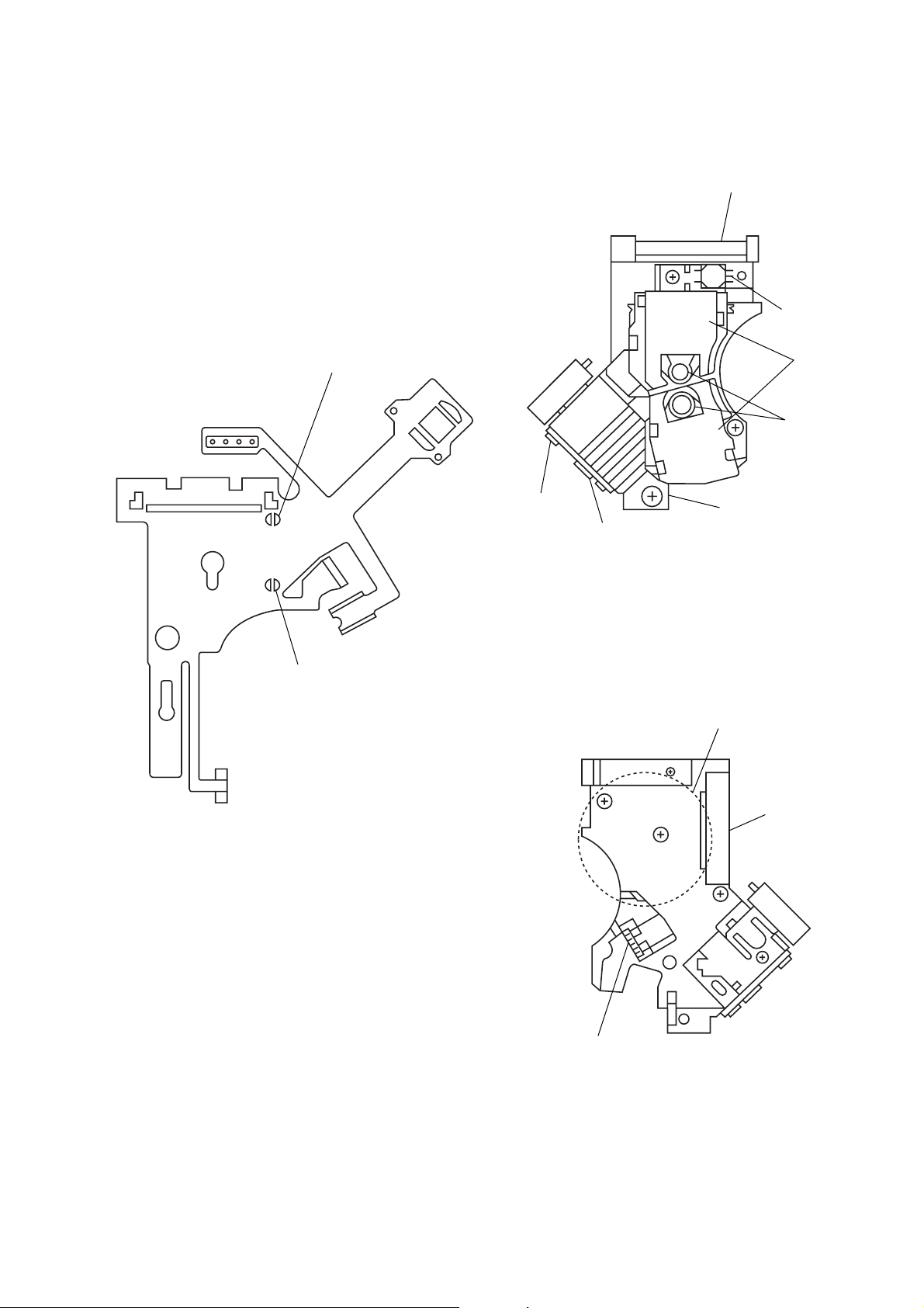
6. REPLACING OPTICAL PICK-UP
6-1. Handling
1) A red laser diode for DVD requires more attention to static
electricity than general infrared laser diodes for CD.
Because its durability to static electricity is far weaker than
that of infrared laser diodes, always use an earth band when
handling the optical pick-up block as service parts.
2) As for the flexible board KHS-180A (RP) packed as service
parts, the short lands have been soldered to protect from static
electricity. Accordingly, remove solders when replacing optical pick-up. (See Fig. 6)
3) In handling the KHS-180A (RP), do not touch inhibited parts
shown in Fig. 7, but grip the slide base bearing and U-shaped
guide.
Slide base bearing
Skew sensor
DVD short land
CD short land
Laser holder
Lens actuator
covers
Objective lenses
U-shaped guide
OEIC
Touch inhibited parts
• Objective lens
• Skew sensor
• Laser holder
• Laser coupler
• Flexible board
• OEIC
• Lens actuator covers
Flexible board
Fig. 6 Flexible board
Connector
Laser coupler
Fig. 7 KHS-180A (RP)
– 7 –
Page 8

7. NOTE ON ASSEMBLING MECHANICAL DECK
7-1. Application of Grease
1) Grease must be applied if the following parts were replaced.
(See Fig. 8)
Note 1: Recommended grease is Foil KG-70MP.
Note 2: In applying grease, take care not to allow grease to
stick to other parts (particularly, rubber belt, spindle
motor, and optical pick-up)
Base unit holder
2 bosses
Slide base Skew cam
Tray 3 grooves
Note:Add grease if tray
moves slowly.
Cam gear
Loading pulley shaft
Note:Add grease if tray
generates noise
periodically.
Fig. 8
– 8 –
Page 9

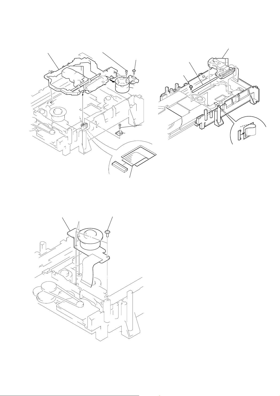
7-2. Cleaning Spindle Motor Turntable
1) Remove the tray. (Refer to 2-7)
2) Clean the spindle motor turntable if disc antiskid rubber (black)
is dirty. (See Fig. 9)
7-4. Deformation of Insulator
1) Assemble the spindle base into the base unit.
2) Lock with 4 shoulder screws. (See Fig. 11)
3) Check if 4 insulators deformed. (See Fig. 11)
Spindle motor
Turntable
Fig. 9
7-3. Aligning Phase of Cam Gear and
Drive Gear
1) Align triangle marks when assembling the cam gear and drive
gear. (See Fig. 10)
Four step screws
Two insulators
Insulator
Two insulators
Good NG
Fig. 11
7-5. Note on Mounting FG-43 Board
1) Align two bosses. (See Fig. 12)
2) Fix the board securely with screws (PTPWH2 × 5). (The sen-
sor will not function normally if the board floats up.)
Drive gear Cam gear
Align triangle marks.
Screw
(PTPWH2 × 5)
FG-43 board
Two bosses
Fig. 10
Fig. 12
– 9 –
Page 10
7-6. Note on Mounting TK-47 Board
1) Align two bosses. (See Fig. 13)
2) Align four tabs. (See Fig. 13)
3) Fix the board securely with 3 screws (BV3 × 10). (The sensor
will not function normally if the board floats up.)
Three screws
TK-47 board
Two claws
(BV3 × 10)
Boss
Two claws
Boss
Fig. 13
7-7. Note on connecting OPT Harness
1) The optical pick-up could be destroyed unless the OPT harness is connected normally to the connector. (See Fig. 14)
OPT harness
Good NG
Connector
Fig. 14
– 10 –
Page 11

SECTION 1
GENERAL
DVP-S300/S305/S315
This section is extracted from
DVP-S315 instruction manual.
1-1
Page 12

1-2
Page 13

1-3
Page 14

1-4
Page 15

1-5
Page 16

1-6
Page 17

1-7
Page 18

1-8
Page 19
1-9
Page 20

1-10
1-10 E
Page 21

DVP-S300/S305/S315
SECTION 2
DISASSEMBLY
Note: Follow the disassembly procedure in the numerical order given.
2-1. CASE REMOVAL 2-3. MB-78 BOARD REMOVAL
7 Cover (upper)
1 Two tapping screws
2 Two tapping screws
4 Case
5 Two screws
(B3)
6 Three screws
(B3)
3 Two tapping screws
2-2. FRONT PANEL SECTION REMOVAL
2 Flat cable
7 Screw
(B3)
0 Claw
1 Connector
(CN001)
1 Two connectors
(CN001, 002)
9 MB-78
0 Four flat cables
(CN101, 252, 301, 452)
2-4. AU-197 BOARD REMOVAL
8 Screw
(B3)
9 Lug
board
4 Two screws
2 Connector
(CN205)
1 Flat cable
(CN202)
(S315)
2 Two flat cables
(CN301, 601)
8 Two screws
(B3)
3 Flat cable
(CN251)
(S315)
4 Connector
(CN361)
(B3)
5 AU-197 board
3 Four screws
(BVTP3 × 12)
5 Two claws
6 Tray ornamental
panel ass’y
!¡ Two claws
4 Draw out the
tray by hand.
!™ Claw
3 Rotate the cam gear
in direction A.
!£ Front panel section
Cam gear
A
6 Two flat cables
(CN201, 203)
2-1
Page 22

2-5. MD BLOCK ASS’Y REMOVAL 2-7. TRAY REMOVAL
3 Chassis
bracket (B)
5 Two screws
(B3)
6 Clamp
1 Cover (lower)
2 Two screws
(B3)
7 MD block ass’y
1 Two screws
(BVTP3 × 10)
2 Press pully bracket
4 Pull the tray.
6 Remove the
tray.
4 Two screws
(B3)
A
5 Claw
3 Rotate the cam gear
in direction A.
2-6. TK-47 BOARD REMOVAL 2-8. SKEW MOTOR (M902) REMOVAL
1 Screw
(PTTWH2 × 5)
3 Skew gear retainer
4 Skew motor
(M902)
2 Flat cable
(spindle
motor)
(CN002)
1 Connector
(CN004)
4 Four screws
(BVTP3 × 10)
6 TK-47 board
3 OP-15
flexible
board
(CN001)
5 Two claws
2 Claw
2-2
Page 23
2-9. SLED MOTOR (M501) REMOVAL 2-11. OPTICAL PICK-UP REMOVAL
4 Spindle base
6 Two screws
(P1.7 × 2.5)
5 Screw
(PTTWH2 × 5)
7 Sled motor
3 Skew shaft
stopper
1 OP-15 flexible
board
(CN001)
4 Optical pick-up
3 Main shaft
2 Screw
(PTTWH2 × 5)
(M501)
2 Screw
(P2 × 8)
1 OP-15 flexible board
(CN001)
2-10. SPINDLE MOTOR (M901) REMOVAL
2 Spindle motor
(M901)
1 Three screws
(PTTWH2 × 5)
2-3
Page 24

2-12. INTERNAL VIEWS
Skew motor ass’y
X-3947-138-1
Optical pick-up
(KHS-180A/J1N)
8-820-005-02
Sled motor ass’y
X-3947-137-1
Sled motor ass’y
X-3947-137-1
Optical pick-up
(KHS-180A/J1N)
8-820-005-02
DC motor
(spindle)
1-698-944-11
DC motor (spindle)
1-698-944-11
Motor (loading)
1-698-942-21
2-4
Page 25

2-13. CIRCUIT BOARDS LOCATION
MB-78
(SIGNAL PROCESS/SERVO)
POWER BLOCK
HS-930SF (S300: E/S305) Taiwan/E
HS-930SH (S315) /S305 Chinese, Singapore
()
HS-930SU (S300: US)
(SWITCHING REGULATOR)
HP-96 (S300/S315)
(HEAD PHONE)
ME-15 (S305)
(MIC IN)
FR-133
(IR/POWER SWITCH)
FG-43
(SLED)
DC MOTOR
(SPINDLE)
FL-88
(FL DRIVER/FUNCTION SWITCH)
AU-197
(AUDIO)
ER-2 (S315)
(EURO AV)
TK-47
(RF/SERVO)
2-5
2-5 E
Page 26

40, 41 AD2, 3 I Input of AD
42 GND – GND
43-46 AD4-7 I Input of AD
47 SDA – Not used
48 SCL – Not used
49-51 GND – GND
52 HSTX – Not used
53 REF V I Input of V SYNC
54 IFCS I Input of SH interrupt signal
55 ST-BY CONT I Input of ST-BY control signal
56 INT3 – Not used
57 CW I Input of JOG control signal
58 CCW I Input of JOG control signa
59 IR I Input of SIRCS
60 A1 IN I Input of control A1 signal
61 A1 OUT O Output of control A1 signal
62 DOT I – Not used
63 AC-3 OUT – Not used
64 STATUS – Not used
65-70 MODEL0-5 I/O Model select1-6
71 1C I/O AC3 indicator
72 1D I/O S-LINK status
73, 74 MIC IN 1, 2 I MIC input select
75, 76 SW2, 3 – Not used
77 RESET IN I EXT RESET request
78-80 RCODE0 I/O REGION set1-3
81 GND – GND
82 X OUT O Output of X’tal(4MHz)
83 X IN I Input of X’tal(4MHz)
84 EVER 5V – Analog power supply
85-92 AD0-7 I/O Address and data set
93-100 A8-15 I/O Set address
5-1. INTERFACE CONTROL PIN FUNCTION (IC604 on MB-78 Board (6/8))
Pin No. Pin Name I/O Function
Pin No. Pin Name I/O Function
1-4 A16-19 I/O Set Address
5, 6 TIN0, 1 – Not used
7, 8 TOT0, 1 – Not used
9 ALE O Output of address latch inable signal
10 OE O Output of output inable signal
11 GND – GND
12 WRL O Output of write inable signal
13 WRH – Not used
14 HRQ – Not used
15 HAK – Not used
16 INTMS I Input of ready signal
17 CLK – Not used
18 RX I Input of serial bus0
19 TX O Output of serial bus0
20 SCK I/O Serialbus0
21 SI – Not used
22 SO O Output of serial bus1
23 EVER 5V – Digital power supply
24 SCLK I/O Serialbus1
25
VIDEO MUTE
O Output of video mute signal
26
AUDIO MUTE
O Output of audio mute signal
27 PPG1 – Not used
28 CGCS O Output of charactor generator chip select
29 FL2CS O Output of FLCS (for 5ch)
30 FLCS O Output of FLCS
31 RESET O RESET
32 PPG6 I Input DIAG
33 P.CONT O Output of POWER CONT signal
34, 35 EVER 5V – Analog power supply
36, 37 GND – GND
38 MIC CONT I Input of MIC CONT signal
39 ECHO CONT I Input of ECHO CONT signal
5-1
IC PIN FUNCTION DESCRIPTION
SECTION 5
DVP-S300/S305/S315
Page 27

1 PB14/IRQ6 I Input of interrupt fromIC506
2 PB15/IRQ7 I Input of interrupt fromIC804
3 VSS – Digital ground
4-11 AD0-7 I/O Data bus AD0-7
12 VSS – Digital ground
13, 14 AD8, 9 I/O Data bus AD8,9
15 VCC – Digital power supply
16-21 AD10-15 I/O Data bus AD10-15
22 VSS – Digital ground
23-30 A0-7 O Address bus A0-7
31 VSS – Digital ground
32-39 A8-15 O Address bus A8-15
40 VSS – Digital ground
41, 42 A16, 17 O Address bus A16,17
43 VCC – Digital power supply
44-47 A18-21 O Address bus A18-21
48 CS0 O Chip select signal for external ROM(ICS803)
49 CS1 O Chip select signal for external ROM(IC802)
50 CS2 – Not used
51 CS3 – Not used
52 VSS – Digital ground
53 PA0/CS4 O Reset signal for IC101,209
54 PA1/CS5 O Output of reset signal
55 PA2/CS6 O Output of chip select signal to IC804
56 WAIT I Input of wait signal
57 WRL/WR O Output of write signal
58 WRH/LBS – Not used
59 RD O Output of read signal
60 PA7/BACK O Output of reset signal to IC508
61 VSS – Digital ground
62 PA8/BREQ O Output of reset signal to IC101
63 PA9 O Output of reset signal to IC506
64 PA10 O Output of A mute signal
65 PA11 O Output of MA mute signal
66 IRQ0 I Input of interrupt fromIC203
67 IRQ1 I Input of DMA request from IC203
68 IRQ2 I Input of V SYNC(FID) interrupt signal
69 IRQ3 I Input of interrupt from IC804
70 VCC – Digital power supply
71 CK O Output of internal clock
72 VSS – Digital ground
73 EXTAL – 20MHz crystal connection pin
74 XTAL – 20MHz crystal connection pin
75
VCC (Vpp)
– Digital power supply
76 NMI I/O Hyper terminal pin
77
VCC
– Digital power supply
78 WDTOVF – Not used
79 RES I Input of reset signal
80 MD0 I Input of mode select0 (fixed to 1)
81 MD1 I Input of mode select1 (fixed to 0)
82 MD2 I Input of mode select2 (fixed to 0)
83, 84 VCC – Digital power supply
85 AVCC – Analog power supply
86 AVREF – Reference power supply
87 PC0/AN0 I/O Set of mode 1
88 PC1/AN1 I/O Set of mode 2
89 PC2/AN2 I/O Set of mode 3
90 PC3/AN3 I/O Set of mode 4
91 AVSS – Analog ground
92 PC4/AN4 I/O Set of mode 5
93 PC5/AN5 I/O Set of mode 6
94 PC6/AN6 – Not used
95 PC7/AN7 – Not used
96 VSS – Digital ground
97 PB0 – HFG
98 PB1 O Output of reset signal for IC806
99 VCC – Digital power supply
100 PB2 O Output of control signal for IC101
5-2. SYSTEM CONTROL PIN FUNCTION (IC805 on MB-78 Board (8/8))
Pin No. Pin Name I/O Function
Pin No. Pin Name I/O Function
5-2
Page 28

101 PB3 – Not used
102 PB4 – Not used
103 PB5 – Not used
104 PB6 – Not used
105 PB7 – Not used
106 VSS – Digital ground
107 RxD0 I Input of serial data
108 TxD0 O Output of serial data
109 RxD1 I Input of serial data
110 TxD1 O Output of serial data
111 SCK0 O Output of serial clock
112 SCK1 O Output of serial clock
Pin No. Pin Name I/O Function
5-3 E
5-3
Page 29

SECTION 6
TEST MODE
DVP-S300/S305/S315
6-1. Starting up Test Mode
With the DVP-S300/S305/S315 turned off, press [TITLE],
[CLEAR], and [POWER] keys on the Remocon in this order, and
the Test mode will start up and the Test Mode Menu as shown in
Figure 1 will appear on the video display.
Test Mode Menu
0. Syscon Diagnosis
1. Drive Auto Adjustment
2. Drive Manual Operation
3. Mecha Aging
4. Emergency History
5. Other Checks
Exit: POWER key
Figure 1
In the Test mode, use all keys on the Remocon or operation panel
when performing necessary operation. In any menu except during
test with the Syscon Diagnosis menu, press the [POWER] key to
exit from the Test mode, and return to the power off status.
Pressing [0] key on the Remocon during display of this initial menu
activates the Diagnosis mode and the screen as shown in Figure 2
appears.
Syscon Diagnosis
IF con Ver. →IFcon version (checksum)
SYScon Ver. →Syscon version (checksum)
(checksum of Syscon is
initially 0000)
Model No. DPX11???? →Model code
** Press Remocon Key **
SIRCS:FF KEY:FF
Figure 2
6-2. Selection of Check Item
A check item can be selected when Model No. is displayed. Press
numeric keys to check the selected item, or any key other than
numeric keys to check all items.
Syscon Diagnosis
IF con Ver. 0.620 (9315)
SYScon Ver. 0.400 (0000)
Select Sub No. ; 02 - →Enter item No.[02]
** Press Remocon Key **
SIRCS:FF KEY:FF
Figure 4
Syscon Diagnosis
IF con Ver. 0.620 (9315)
SYScon Ver. 0.400 (0000)
Select Sub No. ; 02 - 0 →Enter item No.[02-0]
** Press Remocon Key **
SIRCS:FF KEY:FF
Figure 5
Syscon Diagnosis
IF con Ver. 0.620 (9315)
SYScon Ver. 0.400 (0000)
Press Enter ; 02 - 02 →Enter item No.[02-02]
** Press Remocon Key **
SIRCS:FF KEY:FF
Figure 6
Up to here, the [CLEAR] key can be used. Pressing [CLEAR] key
clears the selected number, and selection can be retried from the
beginning. If [ENTER] key is pressed, the diagnosis of only the
selected number is executed, and the result is displayed.
If any key is pressed while the result display is blinking, the screen
returns to the initial Test Mode Menu screen. Where visual check
is necessary such as a still picture check, or when an error occurred, use [PREV] key for repeated checking. To go to the next
step, press [NEXT] key.
If the diagnosis of selected number does not exist, the initial screen
is restored when [ENTER] key is pressed.
6-2-1. Selected Item Check
As the menu is not displayed, select the number from the list, and
enter 2-digit main item No. and 2-digit sub item No. using numeric keys on the Remocon. When the first one digit is entered,
the item selection screen is displayed. Then, enter remaining three
digits and press [ENTER] key.
When an item is selected, the detail check is executed where in
the case of RAM check, all addresses are checked twice by changing the data.
<Example> Select 2-2 ROM Check.
As item No. is <2-2>, enter “0202”.
Syscon Diagnosis
IF con Ver. 0.620 (9315)
SYScon Ver. 0.400 (0000)
Select Diag No. ; 0 - →Enter item No.[0]
** Press Remocon Key **
SIRCS:FF KEY:FF
Figure 3
6-2-2. All Items Check
Press any key other than numeric keys when Model No. is displayed to activate the all items check mode. In the all items check
mode, RAM check is simplified. In concrete, only the skipped
blocks such as 0-ff, 500-5ff, a00-aff, f00-fff, 1400-14ff, ... (addresses) are checked. Check is executed from the top item of the
diagnosis check items list sequentially. In a checking where visual
check is not necessary, check progresses to the next item automatically unless an error occurs.
In case of an error or visual check is necessary, press [PREV] k ey,
and the item concerned is repeatedly checked. To go to the next
item, press [NEXT] key.
6-1
Page 30

6-3. Error Display
(3) Destination Setting
In case of an error, the error code and information are displayed as
shown in Figure 7.
Syscon Diagnosis
IF con Ver. 0.620 (9315)
SYScon Ver. 0.400 (62ED)
RAM Check →Check item name
Error Code: 05 →Error code
Address : 01001D87 →Address where error occurred
Write Data: 20 →Written data (2 – 8 digits)
Read Data: FF →Read data (2 – 8 digits)
SIRCS:FF KEY:FF
Figure 7
When the Error Code is other than “05” (write/read data mismatch
error), the Address and Data become “0”.
“Diag OK” or “Diag Error End” message blinks, when the check
is all finished or stopped. Press a key here, and the screen returns
to the initial Test Mode Menu screen.
6-4. General Description of Checking Method
This section describes briefly a checking method of each diagnosis item, following the order of menu.
The number in ( ) in each item indicates a diagnosis item number.
(2) Memory
(2-2) Syscon ROM (IC803) Check
Checksum calculation
Error: Not detected
At addresses from 0x00000 to 0xfffff of Syscon ROM (IC803),
checksum is calculated by adding 8-bit data, and the result is displayed with 4-digit number in hexadecimal notation. As the error
is not detected, compare the displayed result with original ROM
checksum.
(2-3) Syscon RAM (IC802) Check (DMA used)
Syscon ROM (IC803) → Syscon RAM (IC802) matching check
Error 05: Write/read data mismatch error
External RAM (IC802) of IC805 (Syscon) is saved in the stack by
256 bytes each, and ROM data are transferred to the DMA. Then,
the data are compared with ROM (IC803) data every byte. In detail check, the bit inverted data are further wr itten, and rechecked.
During checking, all interruptions are stopped. Also, variables use
only the stacks including save area and bit inverted buffer. As a
processing is executed in the closed circuits within this function,
the data transfer to stack area also uses the DMA. In the detail
check, all areas of external RAM (IC802) are checked twice by
inverting the data, but in the simple check, one block is checked,
then the subsequent 4 blocks are skipped, and also a check of inverted data is not executed.
If write/read mismatch error occurred, checking can be repeated.
(3-2) Destination setting Check
I/O port read
Error: Not detected
The destination setting port (I/O) is read, and displayed with hex.
number.
Error is not detected.
(4) Gate Array (62000CFh: Peripheral Access Control)
(4-2) Register
Write data → Read data matching check
Error 05: Write/read data mismatch error
Register at adrs=62000CFh (Peripheral Access Control)
Whether written data and read data are matched is checked.
If write/read mismatch error occurred, checking can be repeated.
(4-3) Reset Line
Write → Hard reset → Read
Error 02: Reset error
0xff is written to the register (Peripheral Access Control) at
adrs=62000CFh, and whether it is initialized to “0x00” by the reset pulse is checked.
(5) Drive
(5-2) EEPROM (serial) (IC801)
Data write → Read matching check
Error 05: Write/read data mismatch error
11: Serial transfer error
12: EEPROM not ready
16-bit data is written to the address 0 of EEPROM (IC801), and it
is read to check for matching. Before checking, the content of address 0 is read for saving, but if it cannot be read, the error is
displayed and operation is terminated, and data writing is not executed.
In this diagnosis, 16-bit data is checked. 16 kinds of patterns are
written by shifting 1 bit each from 0x0001 toward the left.
If write/read mismatch error occurred, checking can be repeated.
Even if an error occurs after write/read check started, the saved
data are written when this diagnosis is quitted, but whether data
are written correctly is not guaranteed.
(5-3) SSI (Serial)
Serial register write → Register read matching check
Error 05: Write/read data mismatch error
33: SSI serial transfer error
0x00 – 0xff data are written to the FCCR register for SSI, then
they are read to check for matching.
If write/read mismatch error occurred, checking can be repeated.
6-2
Page 31

(5-4) Servo DSP Download
(6) Data Source
DSP (IC506) code area ROM/RAM discrimination
RAM: Program download → Revision data read
ROM: Revision data read
Error 04: Data read error
13: DSP data not ready
For the Mask ROM, no download can be executed. Download is
possible for the RAM only. ROM/RAM is discriminated by the
DBUSY signal of DSP (IC506) pin 4 after hardware reset. The
diagnosis provides exclusive download flag.
For this flag, download not executed : 0
download already executed: 1
download error : 2
ROM/RAM is discriminated by the status of DBUSY signal after
hardware reset. If RAM, the servo control code is downloaded.
If no error is found, the version No. is read from address:200, and
displayed.
If ROM, the version No. is read from address:200 immediately.
Compare displayed data with existing data.
If RAM, “DSP Download Rev.=xxxx” is displayed.
If ROM, “DSP Mask ROM Rev.=xxxx” is displayed.
(5-5) Servo DSP Register
(Program download) → Data write → Read matching check
(6-2) Register in ARP (IC806)
Register write → Register read matching check
Error 05: Write/read data mismatch error
Data from “0x00” up to “0xff” are written to 12 registers where all
bits can be written and read, then read to check for matching.
If write/read mismatch error occurred, checking can be repeated.
(6-3) Reset Line in ARP (IC806)
Register write → Hard reset → Register read
Error 02: Reset error
05: Write/read data mismatch error
After “0xfe” is written to the INTEN3 register, whether it is initialized to “0x00” by the reset pulse signal is checked.
To make sure, the written data is read to check for matching before reset is executed.
(6-4) DRAM (IC810) in ARP
ROM data → ARP (IC806) → DRAM (IC810) → ARP (IC806)
read matching check
Error 04: Data read error
05: Write/read data mismatch error
13: DSP data not ready
14: DSP download error
The download flag is checked, and if 0, the program is downloaded .
However, in the case of ROM, it is not downloaded.
Unless download error occurs, the content of address 200h of DSP
(IC506) is read for saving, then checking starts. In this check, 16
kinds of patterns are written to the address 200h by shifting 1 bit
each from 0x0001 toward the left, then they are read.
If write/read mismatch error occurred, checking can be repeated.
(5-6) Servo DSP Reset Line
Register write → Hard reset → Register read
Error 02: Reset error
13: DSP data not ready
14: DSP download error
In the case of RAM, this diagnosis checks that the register cannot
be read after hardware reset. Unless download error occurs, the
content of address 200h of DSP (IC506) is read, and after hardware reset, the data is read again for comparison.
The check results in OK, if the register cannot be read, or data are
not matched even if it can be read. The reset error occurs if read
data are same as that before hardware reset.
In the case of ROM, whether the version No. is initialized by the
reset is checked. First, the version No. is read, then its complement is written.
After hardware reset, the data is read again and if it matches the
written data, the reset error occurs.
Error 03: Data write error (ARP (IC806) is not enabled for data
writing)
04: Data read error (ARP (IC806) is not enabled for data
reading)
05: Write/read data mismatch error
ROM (IC803) patterns are copied to all areas to be checked. Each
time 256 bytes are copied, the addresses of copy source (ROM)
are returned by 254 bytes. In detail check, all areas are checked to
verify all bits in DRAM (IC810), then the inverted data are fur ther
checked in the same manner. The b us width of ARP (IC806) is 16
bits. This check program displays addresses in 16 bits.
Overwriting by the shadow can be detected, as the data are written
to all areas, then read. In the detail check, all areas of RAM (IC802)
are checked twice by inver ting the data, while in the simple check
one block is checked, then subsequent 4 blocks are skipped, and
also inverted data are not checked.
If write/read mismatch error occurred, checking can be repeated.
(6-5) Interrupt Line in ARP (IC806)
Data transfer request → Data transfer stop interruption from ARP
(IC806)
Error 21: ARP (IC806) interruption is not detected
AC-3 audio data stored in ROM (IC803) are transferred to the
ARP (IC806), then the designated sector data output stop interruption from ARP (IC806) is detected.
To discriminate the Decrypt (IC811) interruption which is also
sent in the same line, the Decrypt (IC811) interruption is all masked.
6-3
Page 32

(6-6) Register in Decrypt IC (IC811)
(7-3) Reset Line in 64020
Register write → Register read matching check
Error 05: Write/read data mismatch error
0x00 – 0xfc data (lower 2 bits are masked) are written to the interrupt register, then read to check for matching.
If write/read mismatch error occurred, checking can be repeated.
(6-7) Reset of Decrypt IC (IC811)
Register write → Hard reset → Register read
Error 02: Reset error
05: Write/read data mismatch error
After “0xfc” is written to the interrupt register, whether it is initialized to “0x00” by the reset pulse signal is checked.
To make sure, the written data is read to check for matching before reset is executed.
(6-8) Interrupt Line in Decrypt IC (IC811)
ROM (IC803) → ARP (IC806) → Decrypt (IC811)
Error 22: Decrypt (IC811) interruption is not detected
AC-3 audio data stored in ROM (IC803) are transferred to the
Decrypt via ARP (IC806), then the reserv ed data interruption from
Decrypt (IC811) is detected.
T o discriminate the ARP (IC806) inter ruption which is alsosent in
the same line, the ARP (IC806) interruption is allmasked.
(6-9) Reserved Data Head Byte Reading
ROM (IC803) → ARP (IC806) → Decrypt (IC811) reserved data
head byte read matching check
Register write → Hard reset → Register read matching check
Error 02: Reset error
05: Write/read data mismatch error
After “0xff” is written to the Capture/Compare Control Register
0, whether it is initialized to “0x00” by the reset pulse signal is
checked.
To make sure, the written data is read to check for matching before reset is executed.
(7-4) DREQ Signal Line in 64020
AV Decoder (IC203) DMA check
Error 03: Data write error
04: Data read error
05: Write/read data mismatch error
06: DMA transfer DREQ error
07: DMA transfer address error
The connection of DREQ signal line to the AV Decoder (IC203)
is checked through DMA transfer.
If no error is found in DMA transfer, the transferred data are compared with the DRAM (IC810) data read from the register.
(7-5) DRAM in 64020
ROM data → AV Decoder (IC203) → DRAM (IC810) → A V De-
coder (IC203) read matching check
Error 03: Data write error
04: Data read error
05: Write/read data mismatch error
06: DMA transfer DREQ error
07: DMA transfer address error
Error 05: Write/read data mismatch error
22: Decrypt interruption is not detected
AC-3 audio data stored in ROM (IC803) are transferred to the
Decrypt via ARP (IC806), then the reserved data head bytes are
read from Decrypt (IC811) register.
As this audio data consists of 5 sectors, 0, 1, 2, 3, 4 data are written at the head of reserved data of respective sectors.
Whether these data are matched is checked through every sector
interruption.
If write/read mismatch error occurred, checking can be repeated.
(7) AV Decoder (IC203)
(7-2) Register in 64020
Register write → Register read matching check
Error 05: Write/read data mismatch error
“0x00” – “0xff” data are written to 51 registers where all bits can
be written/read, then they are read to check for matching.
If write/read mismatch error occurred, checking can be repeated.
ROM (IC803) patterns are copied to all areas to be checked. Because of large DRAM (IC810) capacity, each time 256 bytes are
copied, the addresses of copy source (ROM) are returned by 255
bytes. In detail check, to verify all bits in DRAM (IC810), the bit
patterns are checked again after inversion. DMA is used when
writing/reading the data. Though the bus width of AV Decoder
(IC203) is 64 bits, the display is given in 8 bits. Namely, actual
address is 1/8 of displayed data, and lower 3 bits indicate the byte
position.
Overwriting by the shadow can be detected, as the data are written
to all areas, then read. In the detail check, all areas of RAM are
checked twice by inverting the data, while in the simple c heck one
block is checked, then subsequent 4 blocks are skipped, and also
inverted data are not checked.
If write/read mismatch error occurred, checking can be repeated.
6-4
Page 33

(7-6) Connection from ARP (IC806) to 64020
(8-4) 1914 Vsync
ROM data → ARP (IC806) → Decrypt (IC811) → AV Decoder
(IC203)
Error 04: Data read error
05: Write/read data mismatch error
06: DMA transfer DREQ error
07: DMA transfer address error
10: Chip-to-chip data transfer error
AC-3 audio data stored in ROM (IC803) are written to the ARP
(IC806), then whether they are transferred to the AV Decoder
(IC203) is checked. If transfer error is not detected, the address of
AV Decoder (IC203) to which data are transferred is displayed on
the terminal.
A part of data transferred to the AV Decoder (IC203) is read into
Syscon RAM (IC802) through DMA, and compared with ROM
(IC803) data.
(7-7) Interrupt Line in 64020
AV Decoder DRAM (IC201, 202) → (DMA COPY) AV Decoder
DRAM (IC201, 202) another area
Error 31: AV Decoder interruption is not detected
Data transfer stop interruption which is generated through
DMA copy of DRAM (IC201, 202) data in AV Decoder (IC203)
to another area is detected.
(8) Video Consumption Concerned
(8-2) 1914 (Serial)
Color bar output (color bar enable command) from V ideo Encoder
(IC252)
CPU measures the 1914 Vsync interrupt cycle.
Error 41: Vsync interruption is not detected
42: Vsync interrupt cycle error
The number of interruption for 200 msec is counted, and if it is 11
to 13 times, this check is OK. It should be 12 times exactly , but ±1
errors are allowable.
(8-5) Still Picture Output (SDRAM (IC201, 202) direct write)
Pattern data → AV Decoder (IC203) → Video Out
Error 31: AV Decoder (IC203) interruption (DMA transfer) is
not detected
The pattern is directly written to the SDRAM (IC201, 202) in AV
Decoder (IC203), then its picture display is checked.
First, the brightness signal data are written by the amount of one
screen while changing every pixel.
For the color difference signals, both Cr and Cb are set to 80h for
monochromic pictures, and the display is turned on.
Then, color difference signal data are written while changing the
data every column.
As both brightness signal data and color difference signal data
take regular patterns, the processing speed is increased through
DMA transfer of the repeated sections.
Further, in detail check the color difference signal data written to
the out of display area are copied through DAM transfer to change
display colors successively.
If no error is found, the message is displayed to prompt for key
entry.
Check the pattern output.
(8-6) Still Picture Output (via ARP (IC806))
Error 11: Serial transfer error
Using the Vsync interruption, serial communication to the Video
Encoder (IC252) starts, and the color bar enable command is transferred to the 1914.
The Vsync interruption and internal serial 1 interruption are used.
If no error is found, the message is displayed to prompt for key
entry.
Check the color bar output.
(8-3) 1914 Read
ID read → Existing data matching check
Error 40: 1914 ID error
The 1914 device ID is read.
Error if the read value is not “1914 (hex)”.
ROM picture data → ARP (IC806) → AV Decoder (IC203) →
Video Out
Error 10: Chip-to-chip data transfer error
ROM (IC803) data are transferred to the AV Decoder (IC203) via
ARP (IC806), and the displayed picture is checked.
If no error is found, the message is displayed to prompt for key
entry.
The output picture is same as the start-up picture.
(8-7) DNR (Serial) (IC251)
ROM picture data → ARP (IC806) → AV Decoder (IC203) →
DNR (IC251) → Video Out (outline)
Error 10: Chip-to-chip data transfer error
Using special diagnostic command, the output still picture is transferred to the DNR (IC251) for checking.
If no error is found, the message is displayed to prompt for key
entry.
This checking is made only for the players with DNR.
The output picture used is same as that in (8-6) Still Picture Output.
The colors will vary extremely, if DNR (IC251) is effective.
For the players without DNR (IC251), the error code 0 is returned.
6-5
Page 34

(8-8) S Terminal DC Check
(8-13) AV CONT Through Check (DVP-S315)
Color bar output by Video Encoder (IC252)
Error 11: Serial transfer error
The color bars are output in the same manner as in (8-2).
After VS signal is turned on/off repeatedly two times, the color
bar output is turned off.
(8-9) EURO-AV Output Check (DVP-S315)
Color bar output by video encoder (IC252)
ROM audio data → ARP (IC806) → AV Decoder (IC203) → 2ch
DAC (IC215) → Analog Audio Out
Error 11: Serial transfer error
10: ARP (IC806) n AV decoder (IC203) transfer error
35: 2ch DAC (IC215) serial transfer interruption is not de-
tected
37: PLL DAC (IC209) serial transfer interruption is not de-
tected
With AV -CONT: “H”, E-V/Y : “H”, E-V/RGB: “H”, video and audio signals are output.
For the video signals, the color bars are output same as in (8-2).
For the audio signals, MPEG audio signals of ROM (IC803) data
are output same as in (9-7).
Color bar output by video encoder
Error 11: Serial transfer error
Input picture is sent as it is from EURO AV2 (CNJ601) to the AV1
(CNJ602).
The color bars are output from the player, same as in (8-2).
As AV-CONT output signal is turned on/of f repeatedly tw o times,
confirm that the picture output is switched between through and
color bar alternately.
(9) Audio Concerned
(9-2) Sampling Frequency 44.1kHz
16.9344MHz oscillation
Error 37: PLL DAC (IC209) serial transfer interruption is not de-
tected
Sampling frequency 44.1kHz is set to the PLL DAC (IC209).
If no error is found, the message is displayed to prompt for key
entry.
Observe the output waveform of IC209 (CXD8696R) SCK02 pin.
(9-3) Sampling Frequency 48kHz
(8-10) Y/C Output Check (DVP-S315)
Color bar output by video encoder
Error 11: Serial transfer error
With AV-CONT: “H”, E-V/Y: “L”, E-V/RGB: “H”, video signals
areoutput.
For the video signals, the color bars are output same as in (8-2).
(8-11) RGB Output Check (DVP-S315)
Color bar output by video encoder
Error 11: Serial transfer error
With AV-CONT: “H”, E-V/Y: “H”, E-V/RGB: “L”, video signals
areoutput.
For the video signals, the color bars are output same as in (8-2).
(8-12) AV CONT Wide Mode Check (DVP-S315)
Color bar output by video encoder
Error 11: Serial transfer error
With AV-CONT: “H”, VS: “H”, video signals are output.
For the video signals, the color bars are output same as in (8-2).
18.4320MHz oscillation
Error 37: PLL DAC (IC209) serial transfer interruption is not de-
tected
Sampling frequency 48kHz is set to the PLL DAC (IC209).
If no error is found, the message is displayed to prompt for key
entry.
Observe the output waveform of IC209 (CXD8696R) SCK02 pin.
(9-4) Sampling Frequency 96kHz
36.8640MHz oscillation
Error 37: PLL DAC (IC209) serial transfer interruption is not de-
tected
Sampling frequency 96kHz is set to the PLL DAC (IC209).
If no error is found, the message is displayed to prompt for key
entry.
Observe the output waveform of IC209 (CXD8696R) SCK02 pin.
6-6
Page 35

(9-5) Audio Digital Output
(9-8) Dual DAC (Serial)
ROM audio data → ARP (IC806) → AV Decoder (IC203) → Digital audio I/F output
Error 10: ARP (IC806) → AV Decoder (IC203) data transfer
error
37: PLL DA C (IC209) serial transfer inter ruption is not de-
tected
AC-3-audio bit stream data stored in ROM (IC803) are transferred
to the AV Decoder (IC203) via ARP (IC806), and output to the
digital audio interface.
If no error is found, the message is displayed to prompt for key
entry.
Analog outputs are muted.
(9-6) Audio Digital Mute
ROM audio data → ARP (IC806) → AV Decoder (IC203) → Digi-
tal Audio I/F output
Error 10: ARP (IC806) → AV Decoder (IC203) data transfer
error
37: PLL DA C (IC209) serial transfer inter ruption is not de-
tected
AC-3-audio bit stream data stored in R OM (IC803) are transferred
to the AV Decoder (IC203) via ARP (IC806), and output to the
Digital Audio Interface. In such a case, the mute signal is turned
on/off alternately while the data are output 4 times.
1st time : Mute off Audible
2nd time: Mute on Not audible
3rd time : Mute off Audible
4th time : Mute on Not audible
If no error is found, the message is displayed to prompt for key
entry.
(9-7) MPEG Audio Analog Output
ROM audio data → ARP (IC806) → AV Decoder (IC203) → 2ch
DAC (IC215) → Analog audio output
Error 10: ARP (IC806) → AV Decoder (IC203) data transfer
error
35: 2ch DAC (IC215) serial transfer interruption is not de-
tected
37: PLL DA C (IC209) serial transfer inter ruption is not de-
tected
ROM audio data → ARP (IC806) → AV Decoder (IC203) → 2ch
DAC (IC215) → Analog audio output (Attenuation)
Error 10: ARP (IC806) → AV Decoder (IC203) data transfer
error
35: 2ch DAC (IC215) serial transfer interruption is not de-
tected
37: PLL DAC (IC209) serial transfer interruption is not de-
tected
MPEG-audio bit stream data stored in ROM (IC803) are transferred to the AV Decoder (IC203) via ARP (IC806), and they are
attenuated by 12dB (–12dB) in the 2ch DA C (IC215), then analog
audio data are output.
If no error is found, the message is displayed to prompt for key
entry.
(9-9) Audio Mute Line
ROM audio data → ARP (IC806) → AV Decoder (IC203) → Ana-
log audio output (Mute)
Error 10: ARP (IC806) → AV Decoder (IC203) data transfer
error
35: 2ch DAC (IC215) serial transfer interruption is not de-
tected
37: PLL DAC (IC209) serial transfer interruption is not de-
tected
MPEG-audio bit stream data stored in ROM (IC803) are transferred to the AV Decoder (IC203) via ARP (IC806), and analog
audio data are output from 2ch DAC (IC215).
In such a case, first the mute by I/O of SH (IC805), then the mute
by setting AV Decoder (IC203), and by setting DAC are turned on
respectively to output low frequency tones.
Finally, the mute is turned off to output high frequency tones.
Checking is finished when high frequency tones are heard.
Low tones will be heard before this checking finished, if the mute
is not effective.
To make sure which mute is not effective, the check should be
repeated while paying attention to the message.
If no error is found, the message is displayed to prompt for key
entry.
MPEG-audio bit stream data stored in ROM (IC803) are transferred to the AV Decoder (IC203) via ARP (IC806), and analog
audio data are output from 2ch DAC (IC215).
If no error is found, the message is displayed to prompt for key
entry.
6-7
Page 36

g Error Codes in Diagnostic Test
01: Mode not supported is selected
02: Reset error
03: Data write error
04: Data read error
05: Write/read data mismatch error
06: DMA transfer DREQ error
07: DMA transfer address error
10: Chip-to-chip data transfer error
11: Serial transfer error
12: EEPROM is not ready
13: DSP data is not ready
14: DSP download error
21: ARP interruption is not detected
22: Decrypt interruption is not detected
31: AVS Decoder interruption is not detected
32: Servo DSP interruption is not detected
33: SSI interruption is not detected
34: DNR interruption is not detected
35: 2ch DAC interruption is not detected
36: EEPROM interruption is not detected
37: PLL DAC interruption is not detected
40: 1914 ID error
41: Vsync interruption is not detected
42: Vsync interrupt cycle error
43: AC-3 DAC (for main) interruption is not detected
44: AC-3 DAC (for center) interruption is not detected
45: AC-3 DAC (for surrounding) interruption is not detected
52: DIR interruption is not detected
53: V-ENC (CXD1914) interruption is not detected
54: Karaoke DSP (CXD2721Q) interruption is not detected
55: AC-3 Decoder interruption is not detected
56: DIR is not locked
57: AC-3 Decoder – SRAM data bus error
58: AC-3 Decoder – SRAM address bus error
60: Effects IC is not ready
61: Effects IC does not become busy
62: Karaoke DSP is not ready
63: Karaoke DSP does not become busy
90: Judged as error by inspector
91: Check of this item is quitted by key entry
92: Check of all items is quitted by key entry
93: Interruption by time over
99: Other errors
6-8
Page 37

Drive Automatic Adjustment Flowchart
Loading
DVD_SL
adjustment
1
Adj. disc selection
Select “ALL”
EEPROM Default Set
Hydet Init
Sled Init
Go To Home Position
Select “ALL” or “SL”
DVD_SL
adjustment
Eject
Place DVD_SL
disc for adj.
YES
YES
NO
NO
FOK Check
OK
Tracking ON
Sled ON
AGC ON
CLVA
Lock Check
OK
Auto Loop Filter Offset
Auto Focus Offset
Auto Tilt Offset
Auto Focus Offset
servo stop
Go To Home Position
LD ON
Spindle start
Tilt ON
Focus ON
NG
NG
STOP
STOP
Loading
Disc T ype Check
OK
LD ON
Spindle start
Tilt ON
Focus ON
FOK Check
OK
sled move
Auto Tracking Offset
1
NG
NG
STOP
FOK Check
OK
Tan-Position
FOK Check
OK
Tracking ON
Sled ON
AGC ON
CLVA
Lock Check
OK
Tangential skew
adjustment
2
10k tj (rev)
NG
NG
NG
STOP
STOP
6-9
3
4
Page 38

DVD_SL
adjustment
CD
3
4 2
adjustment
5
6
Auto Loop Filter Offset
Auto Focus Offset
Auto Tilt Offset
Auto Focus Offset
Auto Focus Gain
Auto Tracking Gain
Auto EQ.
Auto Loop Filter Offset
Pull in Memory
Jitter Check
OK
Servo STOP
Search Check
OK
Eject
Lock screw
NG
NG
NG
STOP
FOK Check
OK
Auto Tracking Offset
FOK Check
OK
Tracking ON
Sled ON
CLVA
Lock Check
OK
Auto Loop Filter Offset
Auto Focus Offset
Auto Focus Gain
Auto Tracking Gain
Auto Loop Filter Offset
Pull in Memory
NG
NG
NG
STOP
STOP
STOP
CD
adjustment
Select “ALL” or “CD”
Disc change
DVD_SL n VD
Go To Home Position
Disc Type Check
Spindle start
YES
Eject
Loading
OK
LD ON
Tilt ON
Focus ON
NO
NG
Servo STOP
Search Check
DVD_DL
adjustment
Select “ALL” or
Disc change
CD n DVD_DL
Go To Home Position
Jitter Check
OK
OK
“ DVD_DL”
YES
Eject
Loading
NG
STOP
NO
5
6
7
8 9
6-10
Page 39

DVD_DL
adjustment
7 10
8
adjustment
DVD_DL
9
Disc T ype Check
OK
LD ON
Spindle start
Tilt ON
Focus ON
FOK Check
OK
sled move
Auto Tracking Offset
FOK Check
OK
Tracking ON
Sled ON
AGC ON
CLVA
NG
NG
NG
STOP
STOP
FOK Check
OK
Tracking ON
Sled ON
CLVA
Lock Check
Layer Check
OK
Auto Focus Offset
Auto Tilt Offset
Auto Focus Offset
Auto Focus Gain
Auto Tracking Gain
Auto EQ.
Pull in Memory
Jitter Check
OK
NG
NG
NG
STOP
STOP
STOP
Lock Check
OK
Auto Focus Offset
Auto Tilt Offset
Auto Focus Offset
Auto Focus Gain
Auto Tracking Gain
Auto EQ.
Layer Check
OK
Jitter Check
OK
Focus Jump (L0 n L1)
10
NG
NG
NG
STOP
STOP
STOP
Servo Stop
Search Check
OK
Eject
Remove disc
Loading
End
NG
STOP
6-11
Page 40

6-5. Drive Auto Adjustment
T-SKEW adjusting screw
The drive can be automatically adjusted, except disc change and
tangential skew adjustment. For a disc, use the disc for adjustment.
In case of abnormality, press the [stop] key to stop adjustment.
If the drive does not stop, prev ent secondary failure by taking proper
action such as disconnection of the power cable. This adjustment
should be made after repair is finished and no trouble is present in
the drive.
A trouble, if present, causes NG and the adjustment to be aborted.
As the secondary failure could occur, perform automatic adjustment after the drive is completely repaired.
With the initial menu displayed, press [1] on standard commander ,
and the screen as shown in Figure 8 will appear.
Drive Auto Adjustment
SA.00000 SI.00 EMG.OO
Select No. ←Blinking
0: All 3: CD
2: DVD SL 4: DVD-DL
STOP: Press STOP Key
The tray opens after the ENTER key is pressed and the initialization is finished. Then, place the D VD_SL disc for adjustment. Press
the ENTER key to start adjustment. During adjustment, the tangential skew adjustment screen is displayed. Make this adjustment
only when the pickup was replaced.
As for adjustment, rotate the T-SKEW adjusting screw on the
pickup so that the displayed jitter becomes minimum (CCW makes
jitter smaller). Avoid extreme rotation or interference of screwdriver with the disc. After adjustment, a message to apply a screw
locking agent will be displayed if jitter value is within the specification. Then, apply a drip of locking agent to the recess of screw.
Hence, change discs following the given messages on OSD, and
the adjustment is finished if there is no problem.
Note that if “All” is selected, the data of previous adjustment are
erased and initial values are set.
Figure 8
If “All” is selected, the screen shown in Figure 9 is displayed.
Drive Auto Adjustment
SA.00000 SI.00 EMG.OO
0: Adjustment ALL
0: All 2: CD
2: DVD SL 3: DVD-DL
START: Press ENTER Key ←Blinking
STOP: Press STOP Key
Figure 9
Figure 10
6-12
Page 41

6-6. Drive Manual Operation
6-6-3. Manual Control 1
In performing manual operation, observe the following points:
Select correct disc type on the Disc Type screen.
First, select “0. Disc TYpe” and execute “7. Hydet init” and “8.
Sled init”. (See Figure 11)
In case of abnormality, press [stop] immediately to stop operation
and turn off the power.
Do not execute Auto Adjust while executing FG Pause.
Also, as these commands are not protected, take care not to press
wrong key.
When PLL is locked, the sector address (or time code) is displayed
on the right side of SA.
6-6-1. Drive Manual Operation Menu Screen
Drive Manual Operation
SA.000000 SI.00 EMG.00
0. Disc Type
1. Manual Control 1
2. Manual Control 2
3. Manual Control 3
4. Manual Adjust 1
5. Manual Adjust 2
6. Auto Adjust
7. Check
Manual Control 1
SA.000000 SI.00 EMG.00
0. LD off 7. CLVA
1. SP off 8. AV
2. Tilt off 9. Home
3. Focus off →. Sled FWD
4. Track off ←. Sled RVS
5. Sled off ↑ . Tilt Up
6. AGC off ↓ . Tilt Down
DVD SL 12cm
Figure 13
On this screen, turn on/off servo operation items necessary for
playing.
Normally, turn on the items from 0 sequentiall y, and normal trace
is executed at CLVA. In the tracking status, the sector address (or
time code (at CD)) is displayed.
If not displayed, the spindle is not locked, which means a failure.
In case of spindle system failure or no RF , the spindle system may
run, overriding the control.
In this case, do not press the CLVA.
Figure 11
This screen provides a menu for manual operation, and you can go
directly to each screen from here. To return to this screen from
each screen, press the RETURN key.
If SET UP button is pressed, the screen returns to the Test Mode
menu.
For switching between respective screens, use the CLEAR key.
6-6-2. Disc Type
Disk type
SA.000000 SI.00 EMG.00
0. DVD SL 12cm 9. Home
1. CD 12cm
2. DVD DL 12cm
3. DVD SL 8cm
4. CD 8cm
5. DVD DL 8cm
6. Disc type check
7. Hydet init
8. Sled init.
DVD SL 12cm
Figure 12
0. LD : Turn on/off the laser diode.
1. SP : Turn on/off the spindle.
At SP ON, the spindle runs in constant velocity mode.
2. TILT : Turn on/off the tilt servo.
3. Focus : Focus searching is executed and focus is turned on.
Operation is terminated if focus is not turned on after
focus search is retried about 3 times.
4. Track : Turn on/off the tracking servo.
5. AGC : Turns on/off the focus error auto gain control by PULL
IN level.
6. Sled : Turn on/off the sled servo.
7. CLVA : Spindle normal servo.
8. CAV : Spindle in constant velocity mode
9. Home : Return to home position.
→. : Move the sled system outside.
Perform this with the tracking turned off.
←. : Move the sled system inside.
Perform this with the tracking turned off.
↑ . : Move the tilt system up.
↓ . : Move the tilt system down.
On this screen, select the type of disc used.
“6. Disc type check” judges the disc loaded. Confirm that judgment result meets the loaded disc type.
Judgment may fail if adjustment is not made yet immediately after EEPROM Default Set. The CD which is not cut up to the CD
detection sensor position is judged as DVD. The optical system
will be damaged if other disc is loaded after selecting DVD DL.
Be sure to set the disc type.
6-13
Page 42

6-6-4. Manual Control 2
Manual Control 2
SA.000000 SI.00 EMG.00
0. Pause off 4. Eject
1. FCS. Srch off 5. Load
3. Tilt_H off
9. LJ1→0 : After layer jump L1→L0, tracking loop turns
on.
→. FWD 1TJ : Jump one track forward.
←. RVS 1TJ : Jump one track reversely.
6-6-6. Manual Adjust 1
Manual Adjust 1
SA.000000 SI.CD EMG.00
DVD SL 12cm
Figure 14
Eject/Load are not used usually, because they can be done with
the Eject button.
0. Pause : Pause is made by executing track jump once per
revolution.
1. FCS.Srch : The focus drive system is checked by applying
same voltage to the focus drive as that in focus
search.
3. Tilt H : Increase tilt gain.
4. Eject : Eject
5. Load : Loading
6-6-5. Manual Control 3
Manual Control 3
SA.000000 SI.00 EMG.00
0. FWD 32TJ 6. FT0→1
1. RVS 32TJ 7. FJ1→0
2. FWD 500TJ 8. LJ0→1
3. RVS 500TJ 9. LJ1→0
4. FWD 10KTJ →. FWD 1TJ
5. RVS 10KTJ ←. RVS 1TJ
DVD SL 12cm
Figure 15
On this screen, track jump, etc. are executed.
Confirm the sector information (SI) to check the DVD_DL layer
jump direction. Even SI means layer 0, or odd SI means layer 1.
When 1TJ or 32TJ is executed, the tracking is turned on, but the
sled becomes just like initialization.
Also, after executing each jump except 1TJ (and FJ1, 2), the CLVA
mode is set.
The optical system will be damaged if make a jump in wrong direction FJ0, FJ1, LJ0 and LJ1.
0. TRK. Off set xx
1. TRK. Off set 2 (DVD)
2. TRK. Gain 2 (CD)
3. Focus Gain
4. TRK. Gain
DVDSL 12cm
Figure 16
On this screen, manual adjustment can be made where jitter measurement is not executed.
0. TRK Offset
1
: Adjust tracking offset.
1. TRK. Offset 2 (DVD): Adjust DVD tracking offset (TO SSI).
Adjusting range is (A1 – AF) with
A1 – A7: +25 to +175 mV,
A8 – AF: 0 to –175mV.
2. TRK Gain 2 (CD) : Adjust simple AGC of CD.
Adjusting range is (88 – C8) with lower
4 bits fixed.
3. Focus Gain : Adjust focus gain.
4. Tracking Gain
1
TRK Off set : In the tracking offset adjustment for DVD, based
2
: Adjust tracking gain.
on the peak and bottom data measured by DSP , the
SSL33P3720A cansels the offset roughly , then the
DSP adjusts it finely.
Here, finely adjusted value is set. As adjustment is
made by DSP only.
DC component of tracking traverse does not
change.
2
TRK Gain : In the tracking gain adjustment for CD, based on
For the CD, only this set value changes.
the peak and bottom data measured by DSP, the
CXA2556 on the sets simple AGC to 5 steps of
–3.2, –1.6, 0, +1.6, +3.2 dB (Auto Tracking Offset), then the DSP makes setting (Auto Tracking
Gain). Here, DSP setting can be made. In the case
of DVD, only DSP setting is executed.
0. FWD 32TJ : Jump 32 track forward (N track jump).
1. RVS 32TJ : Jump 32 track reversely (N track jump).
2. FWD 500TJ : Jump 500 tracks forward (fine search).
3. RVS 500TJ : Jump 500 tracks reversely (fine search).
4. FWD 10KTJ : Jump 10k tracks forward (direct search).
5. RVS 10KTJ : Jump 10k tracks reversely (direct search).
6. FJ0→1 : After layer jump L0→L1, tracking loop does not
turn on.
7. FJ1→0 : After layer jump L1→L0, tracking loop does not
turn on.
8. LJ0→1 : After layer jump L0→L1, tracking loop turns
on.
6-14
Page 43

6-6-7. Manual Adjust 2
Manual Adjust 2
SA.000000 SI.00 EMG.00
0. Jitter on
1. Focus Offset xx
2. Tilt Offset
3. L.F. Offset
$
DVD_SL 12cm
Figure 17
On this screen, manual adjustment can be made where jitter measurement is executed.
0. Jitter : Turn on/off jitter measurement. Jitter will not
be measured unless the drive runs at CLV.
1. Focus Offset : Adjust focus offset.
2. Tilt Offset : Adjust tilt offset.
3. L.F. Offset : Adjust electrical offset in ARP.
30
6-6-8. Auto Adjust
Auto Adjust
SA.000000 SI.00 EMG.00
3. Auto Focus Gain : Adjust focus gain automatically. Adjusted
result is reflected on the EEPROM. Execute
this with CLVA turned on if possible. If
NG, the system will be defective, and repair it.
4. Auto TRK gain : Adjust tracking gain automatically. Adjusted result is reflected on the EEPROM.
Execute this with CLVA turned on if possible. If NG, the system will be defective,
and repair it.
5. Auto EQ : Adjust RF equalizer properly. Adjusted result is not reflected on the EEPROM. Execute this with CLVA turned on.
6. Auto L.F. Offset : Adjusts electrical offset in ARP. The adjusted value is applied to the EEPROM.
During adjustment, lock the CLV.
7. Memorize Pullin : Sets the pull-in level to the EEPROM.
6-6-9. Check
check
SA.000000 SI.00 EMG.00
1. EEPROM Default set (set)
6. EEPROM Data
DVD_SL 12cm
Figure 19
0. Auto TRK. Offset xx xx
1. Auto Tilt Offset
2. Auto Focus Offset
3. Auto Focus Gain
4. Auto TRK. Gain
5. auto EQ
6. Auto L.F. Offset
7. Memorize Pullin
DVD_SL 12cm
Figure 18
On this screen, eacf item can be automaticallyadjusted individually.
Note, however, that there are some restriction.
0. Auto TRK Offset : Adjust tracking offset automatically. Adjusted result is reflected on the EEPROM.
Turn of f tracking with the Focus turned on.
Do not execute this at outside track because
pickup moves outside. In the case of CD,
tracking simple AGC is also adjusted here.
1. Auto Tilt Offset : Adjust tilt offset automatically. Adjusted
result is reflected on the EEPROM. Execute
this with CLVA turned on. If NG, retry this
after focus offset and tangential skew are
adjusted.
2. Auto Focus Offset: Adjust focus offset automatically . Adjusted
result is reflected on the EEPROM. Execute
this with CLVA turned on. If NG, retry this
after tilt offset and tangential skew are adjusted.
On this screen, various checking can be made. Note, howe ver , that
some items such as EEPROM Default set are not recoverable.
1. EEPROM Default set : Use this to set EEPROM set values to
default values. Before executing this, it
is recommended to record current values.
6. EEPROM data : Display EEPROM set values list.
Display is made with HEX numbers
“00” – “FF”.
6-15
Page 44

6-6-10. EEPROM data screen display
EEPROM data
ID No. 00 SL L0 L1
Focus Offset 80 80 80 80
Focus Gain 30 18 30 30
TRK Offset 80 80 80 80
TRK. CONT. ?? ?? ?? ??
TRK Gain 30 30 30 30
Tilt Offset 80 80 80 80
Pullin Level 9e 9f ab ab
EQ. Boost ?? ?? ?? ??
L.F.O ?? ?? ?? ??
SD. ?? HY. ??
CD DVD
Figure 20
This screen displays various set values including adjusted results
stored in the EEPROM.
ID No. : Nothing is displayed (00 is displayed)
Focus Offset : 00 – FF 80 center (DVD_SL)
Focus Gain : 00 – 7F 20 center (DVD_SL)
TRK. Offset : 00 – FF 80 center (DVD_SL)
TRK. CONT. : Refer to Manual adjust 1 Tracking offset 2 and
Tracking gain.
TRK. Gain : 00 – 7F 20 center (DVD_SL)
Tilt Offset : 00 – FF 80 center (DVD_SL)
Pullin Level : 80 – FF D0 center (DVD_SL)
EQ. Boost : Fixed according to the disc type.
L.F.O : Only lower 5 bits are effective.
SD. : About 50 – E0
HY. : About 60 – A0
6-7. Other Operation
For manual operation of the drive, the following operations are
available, besides the operations gi ven on the menu screen. (Common to front panel and remote commander)
Eject/Loading OPEN/CLOSE Stop+Ejection, and Loading
CLEAR CLEAR button
Stop STOP button Servo stop
Retrun RETURN button
Set up SET UP button STOP, then return to test
Cursol key →↑ keys
Cursol key ← keys
Power POWER button Power OFF
Movement throughout the
menu
Return to drive manual operation
mode menu
Increase manually adjusted
value
Decrease manually adjusted
value
6-16
6-16 E
Page 45

SECTION 7
ELECTRICAL ADJUSTMENT
DVP-S300/S305/S315
In making adjustment, refer to 7-4. Adjustment
Related Parts Arrangement.
Note: During diagnostic check, the characters and color bars can
be seen only with the NTSC monitor. Therefore, for diagnostic check, use the monitor that supports both NTSC and
PAL modes
This section describes procedures and instructions necessary for
adjusting electrical circuits in this set.
Instruments required:
1) Color monitor TV
2) Oscilloscope 1 or 2 phenomena, band width over 100 MHz,
with delay mode
3) Frequency counter (over 8 digits)
4) Digital voltmeter
5) Standard commander
6) DVD reference disc
HLX-502 (J-6090-068-A) (dual layer)
HLX-503 (J-6090-069-A) (single layer)
7-1. Power Supply Check
1. HS-930SF/930SH/930SU Board
Mode E-E
Instrument Digital voltmeter
+5.2V Check
Test point CN201 1 pin
Specification 5.2 V ± 0.2 V
+3.3V Check
Test point CN201 4 pin
Specification 3.3 V ± 0.2 V
EVER +5V Check
Test point CN201 6 pin
Specification 5.4 V ± 0.2 V
P_CONT Check
Test point CN201 8 pin
Specification 4V – 5 V
AU +12V Check
Test point CN201 9 pin
Specification 12 V V
AU –12V Check
Test point CN201 !¡ pin
Specification –12 V V
–12V Check
Test point CN201 !™ pin
Specification –12 V V
MTR +12V Check
Test point CN201 !¢ pin
Specification –12 V V
+1.0
–2.0
+2.0
–1.0
+2.0
–1.0
+1.0
–2.0
Checking method:
1) Confirm that each voltage satisfies the specification.
7-1
Page 46

7-2. Adjustment of System Control
1. 27MHz Free Run (MB-78 board)
<Purpose>
27 MHz is the reference clock for the MPEG system, and if it is
not adjusted correctly, checking of 22 MHz and 33 MHz lock in
the following steps will result in NG.
Mode E-E
Test point IC206 8 pin
Instrument Oscilloscope, Frequency counter
Adjusting element CT201
Specification 27000000 ± 100 Hz
Adjusting method:
1) Confirm that the waveform at TP018 is normal.
2) Adjust CT201 to attain 27000000 ± 100 Hz.
Figure 7-1
7-3. Adjustment of Video System
1. Video Level Adjustment (MB-78 board)
<Purpose>
This adjustment is made to satisfy the NTSC Standard, and if not
adjusted correctly, the brightness will be too large or small.
Mode
Signal Color bars
Test point CN252 !¢ pin (terminating 75 Ω)
Instrument Oscilloscope
Adjusting element RV251
Specification 1 ± 0.02 Vp-p
Adjusting method:
1) In the test mode initial menu “0” Syscon Diagnosis, set so that
CXD1914 color bars are generated.
2) Adjust the RV251 to attain 1 ± 0.02 Vp-p.
CXD1914 (ENC) check in test mode
menu “0” Syscon Diagnosis
2. S-terminal Output Check (MB-78 board)
<Purpose>
Check S-terminal video output. If it is incorrect, pictures will not
be displayed correctly in spite of connection to the TV with an Sterminal cable.
Mode CXD1914 (ENC) check in test mode
menu “0” Syscon Diagnosis
Signal Color bars
Test point CN252 0 pin (terminating 75 Ω)
Instrument Oscilloscope
Specification 1 ± 0.05 Vp-p
Checking method:
1) In the test mode initial menu “0” Syscon Diagnosis, set so that
CXD1914 color bars are generated.
2) Confirm that the S-Y level is 1 ± 0.05 Vp-p.
1 ± 0.05 Vp-p
Figure 7-3
3. Checking Component Video Output B-Y
(MB-78 board) (DVP-S315 only)
<Purpose>
This checks component video output B-Y. If it is incorrect, correct colors will not be displayed when connected to, for instance,
projector.
Mode
Signal Color bars
Test point CN251 4 pin (terminating 75 Ω)
Instrument Oscilloscope
Specification 700 ± 30 mVp-p
Checking method:
1) Confirm that the B-Y level is 700 ± 30 mVp-p.
CXD1914 (ENC) check in test mode
menu “0” Syscon Diagnosis
700 ± 30 mVp-p
Figure 7-2
1 ± 0.02 Vp-p
(NTSC)
(PAL)
Figure 7-4
7-2
Page 47

4. Checking Component Video Output R-Y
(MB-78 board) (DVP-S315 only)
<Purpose>
This checks component video output R-Y. If it is incorrect, correct colors will not be displayed when connected to, for instance,
projector.
Mode CXD1914 (ENC) check in test mode
menu “0” Syscon Diagnosis
Signal Color bars
Test point CN251 8 pin (terminating 75 Ω)
Instrument Oscilloscope
Specification 700 ± 30 mVp-p
6. Checking S Video Output S-C (MB-78 board)
<Purpose>
This checks whether the S-C satisfies the NTSC Standard. If it is
not correct, the colors will be too dark or light.
Mode CXD1914 (ENC) check in test mode
menu “0” Syscon Diagnosis
Signal Color bars
Test point CN252 !™ pin
Instrument Oscilloscope
Specification 286 ± 20 mVp-p
Connection:
Checking method:
1) Confirm that the R-Y level is 700 ± 30 mVp-p.
700 ± 30 mVp-p
(NTSC)
(PAL)
Figure 7-5
5. Checking Component Video Output Y
(MB-78 board) (DVP-S315 only)
<Purpose>
This checks component video output Y. If it is incorrect, correct
brightness will not be attained when connected to, for instance,
projector.
Mode
CXD1914 (ENC) check in test mode
menu “0” Syscon Diagnosis
Signal Color bars
Test point CN251 6 pin (terminating 75 Ω)
Instrument Oscilloscope
Specification 1 ± 0.05 Vp-p
Checking method:
1) Confirm that the Y level is 1 ± 0.05 Vp-p.
1 ± 0.05 Vp-p
(NTSC)
12
11
CN252
Oscilloscope
75Ω
±1%
100µF
100k
±1%
+
Checking method:
1) Confirm that the S-C burst is 286 ±20 mVp-p.
286 ± 20 mVp-p
Figure 7-7
7. Checking S Video Output DC Level (MB-78 board)
<Purpose>
This checks signals for S1 and S2 compatible TV. If they are not
correct, the TV will not switch automatically to letter box, etc.
Mode CXD1914 (ENC) check in test mode
menu “0” Syscon Diagnosis
Signal Color bars
Test point CN252 !™ pin
Instrument Digital voltmeter
Specification S-terminal 0V: 0V
S-terminal 5V: 5.0 V
+0
–1.5
Connection:
12
11
CN252
Digital voltmeter
75Ω
±1%
100µF
100k
±1%
+
(PAL)
Figure 7-6
Checking method:
1) In the test mode initial menu “0” Syscon Diagnosis, select Sterminal 0 V.
Confirm that the voltage at CN252 !™ pin is 0 V.
2) Press any key to select S-terminal 5V.
Confirm that the voltage at CN252 !™ pin is 5.0 V.
+0
–1.5
7-3
Page 48

7-4. Adjustment Related Parts Arrangement
MB-78 BOARD (Side A)
RV251
VIDEO
LEVEL
14
17
CT201
27MHz FREERUN
HS-930SF/930SH/930SU BOARD (Side A)
8
IC206
CN251
19
CN201
1
4
6
8
11
14
9
12
7-4
Page 49

MB-78 BOARD (Side B)
CN252
1
2
10
12
14
24
25
7-5 E
Page 50

SECTION 8
REPAIR PARTS LIST
DVP-S300/S305/S315
8-1. EXPLODED VIEWS
NOTE:
• -XX and -X mean standardized parts, so they may
have some difference from the original one.
• Items marked “*” are not stocked since they are
seldom required for routine service. Some delay
should be anticipated when ordering these items.
• Color Indication of Appearance Parts
Example:
KNOB, BALANCE (WHITE) . . . (RED)
↑↑
Parts Color Cabinet's Color
8-1-1. CASE ASSEMBLY
3
5
• The mechanical parts with no reference number in
the exploded views are not supplied.
• Hardware (# mark) list and accessories and packing materials are given in the last of the electrical
parts list.
The components identified by mark
! or dotted line with mark ! are critical for safety.
Replace only with part number specified.
3
4
2
6
1
1 3-970-608-11 SUMITITE (B3), +BV
2 X-3948-369-1 PLATE ASSY, TRAY ORNAMENTAL
(S300/S315)
2 X-3948-382-1 PLATE ASSY, TRAY ORNAMENTAL
(S305: Taiwan, Chinese)
2 X-3948-384-1 PLATE ASSY, TRAY ORNAMENTAL
(S305: E, Singapore)
3 3-710-901-41 SCREW, TAPPING
(S300/S305: E, Singapore/S315)
3 3-710-901-51 SCREW, TAPPING (S305: Taiwan, Chinese)
3
1
not
supplied
Ref. No. Part No. Description RemarkRef. No. Part No. Description Remark
* 4 3-988-027-01 CASE (S300/S315)
* 4 3-988-027-11 CASE (S305: E, Singapore)
* 4 3-988-027-21 CASE (S305: Taiwan, Chinese)
5 1-475-686-51 COMMANDER, STANDARD (RMT-D103E)
(S305)
5 1-475-688-11 COMMANDER, STANDARD (RMT-D105A)
(S300)
5 1-475-688-21 COMMANDER, STANDARD (RMT-D105P)
(S315)
6 3-709-044-01 LID, BATTERY CASE
(for RMT-D103E/D105A/D105P)
8-1
Page 51

8-1-2. FRONT PANEL ASSEMBLY
57
54
56
61
60
62
59
63
not supplied
not
supplied
59
S315
59
69
64
59
58
59
not
supplied
68
67
59
65
59
59
70
59
66
53
55
52
51
51 3-988-015-01 RING, SHUTTLE (S300/S315)
51 3-988-015-11 RING, SHUTTLE (S305: E, Singapore)
51 3-988-015-21 RING, SHUTTLE (S305: Taiwan, Chinese)
52 X-3948-380-1 PANEL ASSY, FRONT (S300)
52 X-3948-381-1 PANEL ASSY, FRONT (S305: Taiwan, Chinese)
52 X-3948-383-1 PANEL ASSY, FRONT (S305: E, Singapore)
52 X-3948-426-1 PANEL ASSY, FRONT (S315)
53 4-977-598-11 CUSHION
54 4-981-435-01 RING (DIA. 50), ORNAMENTAL (S305)
54 4-981-435-11 RING (DIA. 50), ORNAMENTAL (S315)
54 4-981-435-21 RING (DIA. 50), ORNAMENTAL (S300)
* 55 3-988-029-11 ESCUTCHEON, PANEL (S300/S315)
* 55 3-988-029-21 ESCUTCHEON, PANEL (S305: Taiwan, Chinese)
* 55 3-988-029-31 ESCUTCHEON, PANEL (S305: E, Singapore)
56 3-988-036-01 WINDOW, INDICATION
54
53
Ref. No. Part No. Description RemarkRef. No. Part No. Description Remark
58 3-988-031-21 BUTTON, OPEN (S305: Taiwan, Chinese)
59 4-951-620-01 SCREW (2.6X8), +BVTP
60 3-945-284-51 KNOB, VOLUME (S300/S315)
60 3-945-284-61 KNOB, VOLUME (S305: E, Singapore)
60 3-945-284-71 KNOB, VOLUME (S305: Taiwan, Chinese)
61 3-950-989-01 NUT (M7), HEXAGON
* 62 3-684-436-01 PLATE, MOUNT
* 63 A-6065-075-A HP-96 BOARD, COMPLETE (S300)
* 63 A-6065-097-A ME-15 BOARD, COMPLETE (S305)
* 63 A-6065-114-A HP-96 BOARD, COMPLETE (S315)
* 64 A-6065-074-A FR-133 BOARD, COMPLETE
65 1-783-345-11 CABLE, FLAT (FML-5) (20P)
* 66 A-6065-112-A FL-88 BOARD, COMPLETE
67 1-475-685-11 ENCODER, ROTARY
68 3-988-016-01 STICK, CURSOR (S300/S315)
57 4-963-404-21 EMBLEM (5-A), SONY
(S300/S305: E, Singapore/S315)
57 4-963-404-81 EMBLEM (5-A), SONY (S305: Taiwan, Chinese)
58 3-988-031-01 BUTTON, OPEN (S300/S315)
58 3-988-031-11 BUTTON, OPEN (S305: E, Singapore)
68 3-988-016-11 STICK, CURSOR (S305: E, Singapore)
68 3-988-016-21 STICK, CURSOR (S305: Taiwan, Chinese)
69 1-500-386-11 FILTER, CLAMP (FERRITE CORE) (S315)
70 3-989-677-01 HOLDER
8-2
Page 52

8-1-3. CHASSIS ASSEMBLY
102
not
supplied
102
not
supplied
S315
112
not
supplied
102
102
not
supplied
101
102
102
not
supplied
not
supplied
102
102
(S315)
not
supplied
113
107
102
#1
105
Taiwan, Chinese
US
106
AEP, UK, E,
Singapore
107
108
104
not
supplied
110
110
110
102
103
not
supplied
* 101 1-468-287-12 POWER BLOCK (HS-930SU) (S300: US)
* 101 1-468-287-21 POWER BLOCK (HS-930SH)
(S315/S305: Chinese, Singapore)
* 101 1-468-287-31 POWER BLOCK (HS-930SF)
(S300: E/S305: Taiwan, E)
102 3-970-608-11 SUMITITE (B3), +BV
* 103 3-691-950-01 SPACER, P.C.BOARD
104 1-783-348-11 CABLE, FLAT (FME-3) (9P) (S315)
105 1-783-339-11 CABLE, FLAT (FMT-21) (27P)
* 106 A-6065-089-A AU-197 BOARD, COMPLETE (S300: US)
* 106 A-6065-096-A AU-197 BOARD, COMPLETE (S305)
* 106 A-6065-106-A AU-197 BOARD, COMPLETE (S315)
#3
109
111
S315
The components identified by mark
! or dotted line with mark ! are critical for safety.
not
supplied
Ref. No. Part No. Description RemarkRef. No. Part No. Description Remark
107 1-783-343-11 CABLE, FLAT (FMA-4) (25P)
108 1-783-353-11 CABLE, FLAT (FEA-2) (15P) (S315)
* 109 A-6065-108-A ER-2 BOARD, COMPLETE (S315)
! 110 1-777-850-51 CORD, POWER (US)
! 110 1-777-851-41 CORD, POWER (E, Singapore)
! 110 1-782-001-61 CORD, POWER (AEP, UK)
! 110 1-782-692-31 CORD, POWER (Chinese)
! 110 1-777-985-51 CORD, POWER (Taiwan)
* 111 3-490-052-01 LABEL, LASER CLASS (1) (S315)
* 112 3-703-150-11 CLAMP
113 1-500-386-11 FILTER, CLAMP (FERRITE CORE) (S315)
Replace only with part number specified.
* 106 A-6065-092-A AU-197 BOARD, COMPLETE (S300: E)
8-3
Page 53

8-1-4. DVD MECHANISM CHASSIS ASSEMBLY (1)
154
158
160
#3
155
166
161
166
153
151
156
157
152
#3
#7
159
not
supplied
163
162
M902
164
165
#3
151 3-975-090-01 TRAY
152 3-975-073-02 GEAR, CAM
153 3-975-087-01 GEAR, DRIVE
154 3-975-086-01 GEAR, TRAY DRIVING
155 3-975-072-01 GEAR, LOADING (MIDWAY)
156 3-975-071-01 PULLEY, LOADING
157 3-669-596-00 WASHER (2.3), STOPPER
158 3-975-070-01 BELT
159 3-975-085-01 PULLEY, MOTOR
Ref. No. Part No. Description RemarkRef. No. Part No. Description Remark
160 3-975-089-01 BRACKET, PRESS PULLEY
* 161 3-975-074-01 PULLEY, PRESS
162 3-975-077-01 SCREW, BU STOPPER
* 163 3-975-088-01 HOLDER, BASE UNIT
* 164 X-3948-398-1 HOLDER ASSY, MD
* 165 A-6065-077-A TK-47 BOARD, COMPLETE
166 4-981-923-01 SCREW (M), STEP
M902 1-698-942-21 MOTOR (LOADING)
8-4
Page 54

8-1-5. DVD MECHANISM CHASSIS ASSEMBLY (2)
207
206
215
219
218
208
215
209
210
220
215
216
211
212
215
M901
202
203
* 201 3-975-066-01 STOPPER, SKEW SHAFT
* 202 3-975-061-01 INSULATOR
* 203 3-975-056-01 BASE, SPINDLE
204 3-975-058-01 CAM, SKEW
* 205 3-975-063-01 BASE, SLIDE
205
202
202
204
215
213
M501
M903
214
202
#8
201
The components identified by mark
! or dotted line with mark ! are critical for safety.
Replace only with part number specified.
Ref. No. Part No. Description RemarkRef. No. Part No. Description Remark
212 1-783-341-11 CABLE, FLAT (FMF-28) (8P)
* 213 3-975-059-01 RETAINER, SKEW GEAR
214 3-975-057-01 GEAR, SKEW
215 4-974-711-01 SCREW (2X5) (P TYIGHT), (+) PTTWH
216 4-974-725-01 SCREW (M1.7X2.5), P
* 206 3-975-065-01 SHAFT, MAIN
! 207 8-820-005-02 OPTICAL PICK-UP KHS-180A/J1N
208 1-665-390-11 OP-15 FLEXIBLE BOARD
209 3-975-067-01 GEAR, RACK
* 210 3-975-064-01 RETAINER, SLED GEAR
* 211 A-6065-078-A FG-43 BOARD, COMPLETE
218 A-4683-008-A GEAR ASSY, LIMITTER
219 4-974-720-01 GEAR (S-B)
220 4-974-726-01 GEAR (S-A)
M501 X-3947-137-1 MOTOR ASSY, SLED
M901 1-698-944-11 MOTOR, DC (SPINDLE)
M903 X-3947-138-1 MOTOR ASSY, SKEW
8-5
Page 55

DVP-S300/S305/S315
AU-197
8-2. ELECTRICAL PARTS LIST
NOTE:
• Due to standardization, replacements in the
parts list may be different from the parts specified in the diagrams or the components used
on the set.
• -XX and -X mean standardized parts, so they
may have some difference from the original
one.
• RESISTORS
All resistors are in ohms.
METAL: Metal-film resistor.
METAL OXIDE: Metal oxide-film resistor.
F: nonflammable
Ref. No. Part No. Description Remark Ref. No. Part No. Description Remark
* A-6065-092-A AU-197 BOARD, COMPLETE (S300: E)
* A-6065-089-A AU-197 BOARD, COMPLETE (S300: US)
* A-6065-096-A AU-197 BOARD, COMPLETE (S305)
* A-6065-106-A AU-197 BOARD, COMPLETE (S315)
***********************
4-352-844-01 PIN, LEAD, COATING
< CAPACITOR >
C202 1-124-910-11 ELECT 47uF 20% 50V
C202 1-126-023-11 ELECT 100uF 20% 25V
C203 1-124-910-11 ELECT 47uF 20% 50V
C203 1-126-023-11 ELECT 100uF 20% 25V
C204 1-124-910-11 ELECT 47uF 20% 50V
C204 1-124-724-11 ELECT 47uF 20% 50V
C205 1-124-910-11 ELECT 47uF 20% 50V
C205 1-124-724-11 ELECT 47uF 20% 50V
C216 1-164-232-11 CERAMIC CHIP 0.01uF 50V
C217 1-164-232-11 CERAMIC CHIP 0.01uF 50V
C224 1-130-484-00 MYLAR 0.012uF 5% 50V
C225 1-130-484-00 MYLAR 0.012uF 5% 50V
C232 1-136-850-11 FILM 0.1uF 5% 63V
C233 1-164-232-11 CERAMIC CHIP 0.01uF 50V
C234 1-130-467-00 MYLAR 470PF 5% 50V
C235 1-126-926-11 ELECT 1000uF 20% 10V
C236 1-130-467-00 MYLAR 470PF 5% 50V
C239 1-126-967-11 ELECT 47uF 20% 16V
C239 1-124-910-11 ELECT 47uF 20% 50V
C240 1-126-967-11 ELECT 47uF 20% 16V
• Items marked “*” are not stocked since they
are seldom required for routine service.
Some delay should be anticipated when ordering these items.
• SEMICONDUCTORS
In each case, u: µ, for example:
uA. . : µA. . uPA. . : µPA. .
uPB. . : µPB. . uPC. . : µPC. .
uPD. . : µPD. .
• CAPACITORS
uF: µF
• COILS
uH: µH
C269 1-164-232-11 CERAMIC CHIP 0.01uF 50V
C286 1-136-850-11 FILM 0.1uF 5% 63V
(Ref.No.2,000 Series)
(S300/S305)
(S315)
(S300/S305)
(S315)
(S300/S305)
(S315)
(S300/S305)
(S315)
(S300/S305)
(S315)
(S300/S305)
C287 1-136-850-11 FILM 0.1uF 5% 63V
C290 1-117-793-11 MYLAR 330PF 5% 50V
C291 1-117-793-11 MYLAR 330PF 5% 50V
C298 1-164-232-11 CERAMIC CHIP 0.01uF 50V
C299 1-126-967-11 ELECT 47uF 20% 16V
C300 1-164-232-11 CERAMIC CHIP 0.01uF 50V
C301 1-126-964-11 ELECT 10uF 20% 50V
C302 1-126-335-11 ELECT 220uF 20% 10V
C303 1-163-243-11 CERAMIC CHIP 47PF 5% 50V
C303 1-163-227-11 CERAMIC CHIP 10PF 0.5PF 50V
C304 1-163-243-11 CERAMIC CHIP 47PF 5% 50V
C304 1-163-227-11 CERAMIC CHIP 10PF 0.5PF 50V
C305 1-163-243-11 CERAMIC CHIP 47PF 5% 50V
C305 1-163-227-11 CERAMIC CHIP 10PF 0.5PF 50V
C306 1-163-231-11 CERAMIC CHIP 15PF 5% 50V
C312 1-164-004-11 CERAMIC CHIP 0.1uF 10% 25V
C313 1-164-004-11 CERAMIC CHIP 0.1uF 10% 25V
C341 1-164-004-11 CERAMIC CHIP 0.1uF 10% 25V
C342 1-126-935-11 ELECT 470uF 20% 6.3V
C351 1-126-933-11 ELECT 100uF 20% 10V
C352 1-126-933-11 ELECT 100uF 20% 10V
C353 1-126-925-11 ELECT 470uF 20% 10V
C354 1-126-925-11 ELECT 470uF 20% 10V
C355 1-164-004-11 CERAMIC CHIP 0.1uF 10% 25V
C356 1-126-967-11 ELECT 47uF 20% 16V
C357 1-164-004-11 CERAMIC CHIP 0.1uF 10% 25V
C365 1-163-259-91 CERAMIC CHIP 220PF 5% 50V
C367 1-163-009-11 CERAMIC CHIP 0.001uF 10% 50V
C372 1-136-850-11 FILM 0.1uF 5% 63V
The components identified by
mark ! or dotted line with mark
! are critical for safety.
Replace only with part number
specified.
When indicating parts by reference
number, please include the board.
(S300/S305)
(S300/S305)
(S315)
(S300/S305)
(S315)
(S300/S305)
(S315)
(S300: US)
C240 1-124-910-11 ELECT 47uF 20% 50V
C245 1-126-964-11 ELECT 10uF 20% 50V
C264 1-164-232-11 CERAMIC CHIP 0.01uF 50V
(S300/S305)
(S315)
C374 1-126-967-11 ELECT 47uF 20% 16V
< CONNECTOR >
CN201 1-774-769-11 CONNECTOR, FFC/FPC 25P
8-6
Page 56

AU-197
Ref. No. Part No. Description Remark Ref. No. Part No. Description Remark
CN202 1-569-932-31 CONNECTOR, FFC/FPC 15P (S315)
CN203 1-774-769-11 CONNECTOR, FFC/FPC 25P
CN205 1-573-733-11 PIN, CONNECTOR 6P (S300)
CN205 1-573-733-21 PIN, CONNECTOR 6P (S315)
CN206 1-506-484-11 PIN, CONNECTOR 5P (S305)
< DIODE >
D201 8-719-988-62 DIODE 1SS355
D202 8-719-988-62 DIODE 1SS355
D352 8-719-067-40 DIODE STZ6.8N-T146 (S300US)
D354 8-719-016-73 DIODE STZ6.8TT146
D356 8-719-016-73 DIODE STZ6.8TT146
D358 8-719-016-73 DIODE STZ6.8TT146
D361 8-719-016-73 DIODE STZ6.8TT146
D362 8-719-975-40 DIODE RB411D
D363 8-719-975-40 DIODE RB411D
< FERRITE BEAD >
L351 1-414-930-21 INDUCTOR 2.2uH
L352 1-414-930-21 INDUCTOR 2.2uH
L354 1-414-926-21 INDUCTOR 0.47uH
L355 1-412-951-11 INDUCTOR 10uH
L356 1-412-951-11 INDUCTOR 10uH
L357 1-412-951-11 INDUCTOR 10uH
Q201 8-729-424-08 TRANSISTOR UN2111 (S300/S315)
Q202 8-729-216-22 TRANSISTOR 2SA1162
Q205 8-729-023-22 TRANSISTOR 2SD2114KT146
Q206 8-729-023-22 TRANSISTOR 2SD2114KT146
Q214 8-729-140-55 TRANSISTOR 2SK739
Q351 8-729-424-08 TRANSISTOR UN2111
Q352 8-729-421-19 TRANSISTOR UN2213
Q353 8-729-120-28 TRANSISTOR 2SC1623-L5L6
< COIL >
< TRANSISTOR >
FB201 1-414-553-11 INDUCTOR 0UH
FB202 1-414-553-11 INDUCTOR 0UH
FB209 1-414-135-11 INDUCTOR CHIP 0UH (S300/S315)
FB210 1-414-135-11 INDUCTOR CHIP 0UH (S300/S315)
FB211 1-414-135-11 INDUCTOR CHIP 0UH (S300/S315)
FB212 1-414-135-11 INDUCTOR CHIP 0UH (S305)
FB213 1-414-135-11 INDUCTOR CHIP 0UH (S300/S315)
FB214 1-414-135-11 INDUCTOR CHIP 0UH (S300/S315)
FB215 1-414-135-11 INDUCTOR CHIP 0UH (S300/S315)
FB216 1-414-135-11 INDUCTOR CHIP 0UH (S305)
FB217 1-414-135-11 INDUCTOR CHIP 0UH (S305)
FB218 1-414-135-11 INDUCTOR CHIP 0UH (S305)
FB251 1-414-135-11 FERRITE 0UH (S315)
FB252 1-414-135-11 FERRITE 0UH (S315)
FB351 1-414-553-11 INDUCTOR 0UH (S300: US)
FB352 1-414-553-11 INDUCTOR 0UH
FB353 1-414-553-11 INDUCTOR 0UH
FB354 1-414-553-11 INDUCTOR 0UH
FB355 1-414-553-11 INDUCTOR 0UH
FB356 1-414-553-11 INDUCTOR 0UH
FB357 1-414-553-11 INDUCTOR 0UH
FB358 1-414-553-11 INDUCTOR 0UH
FB359 1-414-553-11 INDUCTOR 0UH (S300: US)
< IC >
IC201 8-759-522-17 IC NJM79M09DLA(TE1)
IC202 8-759-284-66 IC NJM78M08DLA(TE1)
IC206 8-759-422-21 IC NJM4580V(TE2)
IC207 8-759-422-21 IC NJM4580V(TE2)
IC214 8-759-422-21 IC NJM4580V(TE2) (S300/S315)
< RESISTOR >
R154 1-216-864-11 METAL CHIP 0 5% 1/16W
(S300: US)
R201 1-216-033-00 METAL CHIP 220 5% 1/10W
R202 1-208-798-11 RES, CHIP 4.7K 0.50% 1/10W
R206 1-216-109-00 METAL CHIP 330K 5% 1/10W
R207 1-216-109-00 METAL CHIP 330K 5% 1/10W
R208 1-216-069-00 METAL CHIP 6.8K 5% 1/10W
R209 1-216-069-00 METAL CHIP 6.8K 5% 1/10W
R213 1-216-071-00 METAL CHIP 8.2K 5% 1/10W
R217 1-216-077-00 METAL CHIP 15K 5% 1/10W
(S305)
R218 1-216-071-00 METAL CHIP 8.2K 5% 1/10W
R219 1-216-077-00 METAL CHIP 15K 5% 1/10W
(S305)
R222 1-208-804-11 RES, CHIP 8.2K 0.50% 1/10W
R223 1-216-047-91 RES, CHIP 820 5% 1/10W
R224 1-216-047-91 RES, CHIP 820 5% 1/10W
R225 1-216-025-91 RES, CHIP 100 5% 1/10W
R226 1-216-053-00 METAL CHIP 1.5K 5% 1/10W
R227 1-216-045-00 METAL CHIP 680 5% 1/10W
R228 1-216-045-00 METAL CHIP 680 5% 1/10W
R229 1-216-053-00 METAL CHIP 1.5K 5% 1/10W
R231 1-216-073-00 METAL CHIP 10K 5% 1/10W
R232 1-216-073-00 METAL CHIP 10K 5% 1/10W
(S300/S315)
R235 1-216-109-00 METAL CHIP 330K 5% 1/10W
R236 1-216-109-00 METAL CHIP 330K 5% 1/10W
R241 1-216-041-00 METAL CHIP 470 5% 1/10W
R242 1-216-041-00 METAL CHIP 470 5% 1/10W
IC215 8-759-526-70 IC CXD8750N-T2
IC217 8-759-324-03 IC HA17431UA-TL
IC351 8-759-522-11 IC BA7660FS-E2
IC352 8-749-921-12 IC GP1F32T (DIGITAL OUT OPTICAL)
< JACK >
J352 1-764-188-21 JACK (SMALL TYPE) (DIA. 3.5) (S-LINK)
(S300: US)
J353 1-779-382-11 JACK, PIN 1P (DIGITAL OUT COAXIAL)
J354 1-694-409-41 TERMINAL BOARD (LINE OUT) (S300/S305)
J354 1-694-408-41 TERMINAL BOARD (LINE OUT) (S315)
R249 1-216-073-00 METAL CHIP 10K 5% 1/10W
R250 1-216-097-91 RES, CHIP 100K 5% 1/10W
R254 1-208-805-11 RES, CHIP 9.1K 0.50% 1/10W
R262 1-216-296-91 SHORT 0
R269 1-216-097-91 RES, CHIP 100K 5% 1/10W
R270 1-216-049-91 RES, CHIP 1K 5% 1/10W
R271 1-216-049-91 RES, CHIP 1K 5% 1/10W
R284 1-216-025-91 RES, CHIP 100 5% 1/10W
(S300/S315)
R285 1-216-025-91 RES, CHIP 100 5% 1/10W
(S300/S315)
R298 1-216-025-91 RES, CHIP 100 5% 1/10W
(S300/S315)
8-7
Page 57

AU-197 ER-2
Ref. No. Part No. Description Remark Ref. No. Part No. Description Remark
R384 1-216-295-91 SHORT 0
R305 1-216-025-91 RES, CHIP 100 5% 1/10W
(S300/S315)
R314 1-216-041-00 METAL CHIP 470 5% 1/10W
(S305)
R315 1-216-041-00 METAL CHIP 470 5% 1/10W
(S305)
R315 1-216-009-00 METAL CHIP 22 5% 1/10W
(S315)
R316 1-216-041-00 METAL CHIP 470 5% 1/10W
(S305)
R317 1-216-041-00 METAL CHIP 470 5% 1/10W
(S305)
R317 1-216-009-00 METAL CHIP 22 5% 1/10W
(S315)
R318 1-216-025-91 RES, CHIP 100 5% 1/10W
R319 1-216-025-91 RES, CHIP 100 5% 1/10W
R320 1-216-025-91 RES, CHIP 100 5% 1/10W
R326 1-216-295-91 SHORT 0
R332 1-216-025-91 RES, CHIP 100 5% 1/10W
R333 1-216-049-91 RES, CHIP 1K 5% 1/10W
R333 1-216-817-11 METAL CHIP 470 5% 1/16W
(S300: US/S305: E, Singapore)
R334 1-216-295-91 SHORT 0
R335 1-216-295-91 SHORT 0
R336 1-216-295-91 SHORT 0
R337 1-216-295-91 SHORT 0
R338 1-216-295-91 SHORT 0
R339 1-216-295-91 SHORT 0
R350 1-216-057-00 METAL CHIP 2.2K 5% 1/10W
R351 1-216-021-00 METAL CHIP 68 5% 1/10W
R352 1-216-021-00 METAL CHIP 68 5% 1/10W
R353 1-216-021-00 METAL CHIP 68 5% 1/10W
R354 1-216-021-00 METAL CHIP 68 5% 1/10W
R355 1-216-021-00 METAL CHIP 68 5% 1/10W
R356 1-216-021-00 METAL CHIP 68 5% 1/10W
R357 1-216-057-00 METAL CHIP 2.2K 5% 1/10W
R358 1-216-073-00 METAL CHIP 10K 5% 1/10W
R359 1-216-057-00 METAL CHIP 2.2K 5% 1/10W
R360 1-216-073-00 METAL CHIP 10K 5% 1/10W
R361 1-216-295-91 SHORT 0
R362 1-216-295-91 SHORT 0
R363 1-216-033-00 METAL CHIP 220 5% 1/10W
R364 1-216-021-00 METAL CHIP 68 5% 1/10W
R365 1-216-295-91 SHORT 0
R366 1-216-295-91 SHORT 0
R367 1-216-295-91 SHORT 0
R368 1-216-049-91 RES, CHIP 1K 5% 1/10W
(S300: US)
R369 1-216-025-91 RES, CHIP 100 5% 1/10W
R370 1-216-295-91 SHORT 0
R373 1-216-037-00 METAL CHIP 330 5% 1/10W
R374 1-216-037-00 METAL CHIP 330 5% 1/10W
R375 1-216-037-00 METAL CHIP 330 5% 1/10W
R376 1-216-017-91 RES, CHIP 47 5% 1/10W
R377 1-216-017-91 RES, CHIP 47 5% 1/10W
R378 1-216-017-91 RES, CHIP 47 5% 1/10W
R379 1-216-017-91 RES, CHIP 47 5% 1/10W
R380 1-216-017-91 RES, CHIP 47 5% 1/10W
R381 1-216-017-91 RES, CHIP 47 5% 1/10W
R382 1-216-017-91 RES, CHIP 47 5% 1/10W
R383 1-216-017-91 RES, CHIP 47 5% 1/10W
R385 1-216-295-91 SHORT 0
R386 1-216-295-91 SHORT 0 (S315)
* A-6065-108-A ER-2 BOARD, COMPLETE (S315)
*********************
(Ref.No.2,000 Series)
< CAPACITOR >
C601 1-164-232-11 CERAMIC CHIP 0.01uF 50V
C602 1-128-551-11 ELECT 22uF 20% 25V
C603 1-126-967-11 ELECT 47uF 20% 16V
C604 1-126-967-11 ELECT 47uF 20% 16V
C605 1-164-232-11 CERAMIC CHIP 0.01uF 50V
C606 1-164-232-11 CERAMIC CHIP 0.01uF 50V
C607 1-126-967-11 ELECT 47uF 20% 16V
C608 1-126-967-11 ELECT 47uF 20% 16V
C609 1-164-004-11 CERAMIC CHIP 0.1uF 10% 25V
C610 1-164-004-11 CERAMIC CHIP 0.1uF 10% 25V
C611 1-164-232-11 CERAMIC CHIP 0.01uF 50V
C612 1-164-004-11 CERAMIC CHIP 0.1uF 10% 25V
C613 1-164-004-11 CERAMIC CHIP 0.1uF 10% 25V
C614 1-126-967-11 ELECT 47uF 20% 16V
C615 1-164-232-11 CERAMIC CHIP 0.01uF 50V
C616 1-164-232-11 CERAMIC CHIP 0.01uF 50V
C619 1-126-967-11 ELECT 47uF 20% 16V
C620 1-128-551-11 ELECT 22uF 20% 25V
C622 1-128-551-11 ELECT 22uF 20% 25V
C623 1-126-967-11 ELECT 47uF 20% 16V
C624 1-126-967-11 ELECT 47uF 20% 16V
C625 1-128-551-11 ELECT 22uF 20% 25V
C626 1-128-551-11 ELECT 22uF 20% 25V
C629 1-126-967-11 ELECT 47uF 20% 16V
C630 1-126-967-11 ELECT 47uF 20% 16V
C631 1-164-004-11 CERAMIC CHIP 0.1uF 10% 25V
C632 1-164-004-11 CERAMIC CHIP 0.1uF 10% 25V
C633 1-164-004-11 CERAMIC CHIP 0.1uF 10% 25V
C634 1-164-004-11 CERAMIC CHIP 0.1uF 10% 25V
C637 1-164-232-11 CERAMIC CHIP 0.01uF 50V
C638 1-126-967-11 ELECT 47uF 20% 16V
C639 1-126-967-11 ELECT 47uF 20% 16V
C640 1-164-232-11 CERAMIC CHIP 0.01uF 50V
C641 1-164-232-11 CERAMIC CHIP 0.01uF 50V
C642 1-128-551-11 ELECT 22uF 20% 25V
C645 1-126-933-11 ELECT 100uF 20% 10V
C646 1-128-551-11 ELECT 22uF 20% 25V
C647 1-126-933-11 ELECT 100uF 20% 10V
C648 1-128-551-11 ELECT 22uF 20% 25V
C649 1-126-933-11 ELECT 100uF 20% 10V
C650 1-128-551-11 ELECT 22uF 20% 25V
C651 1-164-232-11 CERAMIC CHIP 0.01uF 50V
C652 1-126-967-11 ELECT 47uF 20% 16V
C664 1-163-133-00 CERAMIC CHIP 470PF 5% 50V
C665 1-163-133-00 CERAMIC CHIP 470PF 5% 50V
C666 1-163-133-00 CERAMIC CHIP 470PF 5% 50V
C667 1-163-133-00 CERAMIC CHIP 470PF 5% 50V
C668 1-163-133-00 CERAMIC CHIP 470PF 5% 50V
C669 1-163-133-00 CERAMIC CHIP 470PF 5% 50V
C670 1-163-133-00 CERAMIC CHIP 470PF 5% 50V
C671 1-163-133-00 CERAMIC CHIP 470PF 5% 50V
8-8
Page 58

ER-2
Ref. No. Part No. Description Remark Ref. No. Part No. Description Remark
C675 1-163-251-11 CERAMIC CHIP 100PF 5% 50V
C676 1-163-251-11 CERAMIC CHIP 100PF 5% 50V
C686 1-163-251-11 CERAMIC CHIP 100PF 5% 50V
C687 1-163-251-11 CERAMIC CHIP 100PF 5% 50V
C694 1-163-009-11 CERAMIC CHIP 0.001uF 10% 50V
C695 1-163-009-11 CERAMIC CHIP 0.001uF 10% 50V
C696 1-128-551-11 ELECT 22uF 20% 25V
C697 1-126-933-11 ELECT 100uF 20% 10V
C698 1-128-551-11 ELECT 22uF 20% 25V
C699 1-126-933-11 ELECT 100uF 20% 10V
C700 1-126-967-11 ELECT 47uF 20% 16V
C701 1-164-232-11 CERAMIC CHIP 0.01uF 50V
< CONNECTOR >
CN601 1-506-482-11 PIN, CONNECTOR 3P
CN602 1-779-647-41 CONNECTOR, FFC/FPC 15P
CN603 1-779-934-11 CONNECTOR, FFC/FPC 9P
< JACK >
CNJ601 1-568-016-51 SOCKET, PIN 21P (EURO AV2)
CNJ602 1-568-016-51 SOCKET, PIN 21P (EURO AV1)
< DIODE >
D601 8-719-404-49 DIODE MA111
D602 8-719-067-40 DIODE STZ6.8N-T146
D603 8-719-067-40 DIODE STZ6.8N-T146
D604 8-719-067-40 DIODE STZ6.8N-T146
D605 8-719-067-40 DIODE STZ6.8N-T146
FB720 1-414-553-11 FERRITE 0UH
FB721 1-414-553-11 FERRITE 0UH
FB722 1-414-553-11 FERRITE 0UH
FB723 1-414-553-11 FERRITE 0UH
FB724 1-414-553-11 FERRITE 0UH
FB725 1-414-553-11 FERRITE 0UH
FB726 1-414-553-11 FERRITE 0UH
FB727 1-414-553-11 FERRITE 0UH
FB728 1-414-553-11 FERRITE 0UH
FB729 1-414-553-11 FERRITE 0UH
FB730 1-414-553-11 FERRITE 0UH
FB731 1-414-553-11 FERRITE 0UH
FB732 1-414-553-11 FERRITE 0UH
FB733 1-414-553-11 FERRITE 0UH
FB734 1-414-553-11 FERRITE 0UH
< IC >
IC601 8-759-446-66 IC MM1113XFBE
IC602 8-759-432-78 IC MM1111XFBE
IC603 8-759-522-11 IC BA7660FS-E2
IC604 8-759-100-96 IC uPC4558G2
IC607 8-759-522-11 IC BA7660FS-E2
IC608 8-759-100-96 IC uPC4558G2
< COIL >
L601 1-414-940-21 INDUCTOR 100uH
L602 1-414-940-21 INDUCTOR 100uH
L603 1-414-940-21 INDUCTOR 100uH
L604 1-414-940-21 INDUCTOR 100uH
D606 8-719-067-40 DIODE STZ6.8N-T146
D607 8-719-067-40 DIODE STZ6.8N-T146
D608 8-719-067-40 DIODE STZ6.8N-T146
D609 8-719-067-40 DIODE STZ6.8N-T146
D610 8-719-067-40 DIODE STZ6.8N-T146
D611 8-719-067-40 DIODE STZ6.8N-T146
D612 8-719-067-40 DIODE STZ6.8N-T146
D613 8-719-067-40 DIODE STZ6.8N-T146
D614 8-719-067-40 DIODE STZ6.8N-T146
D615 8-719-067-40 DIODE STZ6.8N-T146
D616 8-719-067-40 DIODE STZ6.8N-T146
D617 8-719-067-40 DIODE STZ6.8N-T146
D618 8-719-067-40 DIODE STZ6.8N-T146
D619 8-719-067-40 DIODE STZ6.8N-T146
D620 8-719-105-99 DIODE RD6.2M-B1
D621 8-719-977-40 DIODE UDZ-TE-17-13B
D622 8-719-105-99 DIODE RD6.2M-B1
D623 8-719-977-40 DIODE UDZ-TE-17-13B
D624 8-719-105-99 DIODE RD6.2M-B1
D625 8-719-404-49 DIODE MA111
D626 8-719-404-49 DIODE MA111
D627 8-719-404-49 DIODE MA111
D628 8-719-404-49 DIODE MA111
D631 8-719-404-49 DIODE MA111
D632 8-719-404-49 DIODE MA111
< FERRITE BEAD >
< TRANSISTOR >
Q601 8-729-421-19 TRANSISTOR UN2213
Q602 8-729-421-19 TRANSISTOR UN2213
Q604 8-729-023-22 TRANSISTOR 2SD2114KT146
Q605 8-729-023-22 TRANSISTOR 2SD2114KT146
Q606 8-729-421-19 TRANSISTOR UN2213
Q607 8-729-023-22 TRANSISTOR 2SD2114KT146
Q608 8-729-023-22 TRANSISTOR 2SD2114KT146
Q612 8-729-424-18 TRANSISTOR UN2113
Q614 8-729-023-22 TRANSISTOR 2SD2114KT146
Q615 8-729-023-22 TRANSISTOR 2SD2114KT146
Q621 8-729-424-18 TRANSISTOR UN2113
Q622 8-729-023-22 TRANSISTOR 2SD2114KT146
Q623 8-729-023-22 TRANSISTOR 2SD2114KT146
Q624 8-729-424-18 TRANSISTOR UN2113
Q625 8-729-023-22 TRANSISTOR 2SD2114KT146
Q626 8-729-023-22 TRANSISTOR 2SD2114KT146
Q627 8-729-421-19 TRANSISTOR UN2213
Q628 8-729-422-27 TRANSISTOR 2SD601A-Q
Q629 8-729-422-27 TRANSISTOR 2SD601A-Q
Q630 8-729-421-19 TRANSISTOR UN2213
Q632 8-729-422-27 TRANSISTOR 2SD601A-Q
Q633 8-729-023-22 TRANSISTOR 2SD2114KT146
Q634 8-729-023-22 TRANSISTOR 2SD2114KT146
Q635 8-729-424-38 TRANSISTOR UN2110
Q636 8-729-424-28 TRANSISTOR UN2116
FB602 1-414-135-11 FERRITE 0UH
FB603 1-414-135-11 FERRITE 0UH
FB717 1-414-553-11 FERRITE 0UH
FB718 1-414-553-11 FERRITE 0UH
FB719 1-414-553-11 FERRITE 0UH
Q637 8-729-421-19 TRANSISTOR UN2213
Q638 8-729-421-19 TRANSISTOR UN2213
Q639 8-729-422-27 TRANSISTOR 2SD601A-Q
Q640 8-729-421-19 TRANSISTOR UN2213
Q641 8-729-421-19 TRANSISTOR UN2213
8-9
Page 59

ER-2 FG-43
Ref. No. Part No. Description Remark Ref. No. Part No. Description Remark
< RESISTOR >
R675 1-216-049-91 RES, CHIP 1K 5% 1/10W
R601 1-216-295-91 SHORT 0
R603 1-216-295-91 SHORT 0
R604 1-216-295-91 SHORT 0
R605 1-216-295-91 SHORT 0
R606 1-216-295-91 SHORT 0
R607 1-216-295-91 SHORT 0
R608 1-216-295-91 SHORT 0
R609 1-216-097-91 RES, CHIP 100K 5% 1/10W
R610 1-216-097-91 RES, CHIP 100K 5% 1/10W
R611 1-216-081-00 METAL CHIP 22K 5% 1/10W
R612 1-216-081-00 METAL CHIP 22K 5% 1/10W
R613 1-216-295-91 SHORT 0
R614 1-216-077-00 METAL CHIP 15K 5% 1/10W
R615 1-216-077-00 METAL CHIP 15K 5% 1/10W
R616 1-216-049-91 RES, CHIP 1K 5% 1/10W
R617 1-216-049-91 RES, CHIP 1K 5% 1/10W
R618 1-216-295-91 SHORT 0
R619 1-216-073-00 METAL CHIP 10K 5% 1/10W
R620 1-216-073-00 METAL CHIP 10K 5% 1/10W
R621 1-216-073-00 METAL CHIP 10K 5% 1/10W
R622 1-216-073-00 METAL CHIP 10K 5% 1/10W
R623 1-216-049-91 RES, CHIP 1K 5% 1/10W
R624 1-216-049-91 RES, CHIP 1K 5% 1/10W
R625 1-216-095-00 METAL CHIP 82K 5% 1/10W
R626 1-216-095-00 METAL CHIP 82K 5% 1/10W
R676 1-216-049-91 RES, CHIP 1K 5% 1/10W
R679 1-216-079-00 METAL CHIP 18K 5% 1/10W
R680 1-216-069-00 METAL CHIP 6.8K 5% 1/10W
R681 1-216-089-91 RES, CHIP 47K 5% 1/10W
R682 1-216-069-00 METAL CHIP 6.8K 5% 1/10W
R683 1-216-079-00 METAL CHIP 18K 5% 1/10W
R684 1-216-065-91 RES, CHIP 4.7K 5% 1/10W
R685 1-216-065-91 RES, CHIP 4.7K 5% 1/10W
R686 1-216-093-00 METAL CHIP 68K 5% 1/10W
R688 1-216-113-00 METAL CHIP 470K 5% 1/10W
R689 1-216-113-00 METAL CHIP 470K 5% 1/10W
R690 1-216-049-91 RES, CHIP 1K 5% 1/10W
R691 1-216-041-00 METAL CHIP 470 5% 1/10W
R692 1-216-041-00 METAL CHIP 470 5% 1/10W
R700 1-216-049-91 RES, CHIP 1K 5% 1/10W
R701 1-216-049-91 RES, CHIP 1K 5% 1/10W
R704 1-216-049-91 RES, CHIP 1K 5% 1/10W
R706 1-216-021-00 METAL CHIP 68 5% 1/10W
R707 1-216-021-00 METAL CHIP 68 5% 1/10W
R708 1-216-022-00 METAL CHIP 75 5% 1/10W
R709 1-216-022-00 METAL CHIP 75 5% 1/10W
R714 1-216-089-91 RES, CHIP 47K 5% 1/10W
R715 1-216-089-91 RES, CHIP 47K 5% 1/10W
R719 1-216-065-91 RES, CHIP 4.7K 5% 1/10W
R735 1-216-022-00 METAL CHIP 75 5% 1/10W
R628 1-216-095-00 METAL CHIP 82K 5% 1/10W
R629 1-216-073-00 METAL CHIP 10K 5% 1/10W
R631 1-216-079-00 METAL CHIP 18K 5% 1/10W
R632 1-216-069-00 METAL CHIP 6.8K 5% 1/10W
R633 1-216-113-00 METAL CHIP 470K 5% 1/10W
R634 1-216-113-00 METAL CHIP 470K 5% 1/10W
R635 1-216-069-00 METAL CHIP 6.8K 5% 1/10W
R636 1-216-079-00 METAL CHIP 18K 5% 1/10W
R637 1-216-022-00 METAL CHIP 75 5% 1/10W
R638 1-216-113-00 METAL CHIP 470K 5% 1/10W
R639 1-216-113-00 METAL CHIP 470K 5% 1/10W
R640 1-216-041-00 METAL CHIP 470 5% 1/10W
R641 1-216-041-00 METAL CHIP 470 5% 1/10W
R642 1-216-113-00 METAL CHIP 470K 5% 1/10W
R644 1-216-049-91 RES, CHIP 1K 5% 1/10W
R645 1-216-049-91 RES, CHIP 1K 5% 1/10W
R646 1-216-097-91 RES, CHIP 100K 5% 1/10W
R647 1-216-295-91 SHORT 0
R648 1-216-295-91 SHORT 0
R649 1-216-295-91 SHORT 0
R655 1-216-097-91 RES, CHIP 100K 5% 1/10W
R656 1-216-097-91 RES, CHIP 100K 5% 1/10W
R659 1-216-081-00 METAL CHIP 22K 5% 1/10W
R660 1-216-081-00 METAL CHIP 22K 5% 1/10W
R665 1-216-077-00 METAL CHIP 15K 5% 1/10W
R736 1-216-022-00 METAL CHIP 75 5% 1/10W
R738 1-216-113-00 METAL CHIP 470K 5% 1/10W
R739 1-216-022-00 METAL CHIP 75 5% 1/10W
R740 1-216-022-00 METAL CHIP 75 5% 1/10W
R742 1-216-025-91 RES, CHIP 100 5% 1/10W
R744 1-216-017-91 RES, CHIP 47 5% 1/10W
R747 1-216-035-00 METAL CHIP 270 5% 1/10W
R748 1-216-035-00 METAL CHIP 270 5% 1/10W
R749 1-216-037-00 METAL CHIP 330 5% 1/10W
R750 1-216-037-00 METAL CHIP 330 5% 1/10W
R753 1-216-049-91 RES, CHIP 1K 5% 1/10W
R754 1-216-089-91 RES, CHIP 47K 5% 1/10W
R755 1-216-049-91 RES, CHIP 1K 5% 1/10W
< RELAY >
RY601 1-515-622-11 RELAY
RY602 1-515-622-11 RELAY
* A-6065-078-A FG-43 BOARD, COMPLETE
*********************
(Ref.No.3,000 Series)
< CONNECTOR >
CN501 1-784-684-11 CONNECTOR, FFC/FPC 8P
R666 1-216-077-00 METAL CHIP 15K 5% 1/10W
R667 1-216-049-91 RES, CHIP 1K 5% 1/10W
R668 1-216-049-91 RES, CHIP 1K 5% 1/10W
R669 1-216-073-00 METAL CHIP 10K 5% 1/10W
R670 1-216-073-00 METAL CHIP 10K 5% 1/10W
R671 1-216-073-00 METAL CHIP 10K 5% 1/10W
R672 1-216-073-00 METAL CHIP 10K 5% 1/10W
R673 1-216-073-00 METAL CHIP 10K 5% 1/10W
R674 1-216-073-00 METAL CHIP 10K 5% 1/10W
< IC >
IC501 8-719-052-42 IC ELEMENT, HOLE HW-108A-FT(D)
IC502 8-719-052-42 IC ELEMENT, HOLE HW-108A-FT(D)
8-10
Page 60

FL-88
Ref. No. Part No. Description Remark Ref. No. Part No. Description Remark
* A-6065-112-A FL-88 BOARD, COMPLETE
*********************
(Ref.No.2,000 Series)
R115 1-216-073-00 METAL CHIP 10K 5% 1/10W
R116 1-216-073-00 METAL CHIP 10K 5% 1/10W
R117 1-216-037-00 METAL CHIP 330 5% 1/10W
* 3-988-021-01 HOLDER, FL
< CAPACITOR >
C101 1-126-205-11 ELECT CHIP 47uF 20% 6.3V
C102 1-164-232-11 CERAMIC CHIP 0.01uF 50V
C103 1-126-205-11 ELECT CHIP 47uF 20% 6.3V
C104 1-165-319-11 CERAMIC CHIP 0.1uF 50V
C105 1-126-400-11 ELECT 22uF 20% 35V
C106 1-126-603-11 ELECT CHIP 4.7uF 20% 35V
C107 1-164-489-11 CERAMIC CHIP 0.22uF 10% 16V
C109 1-163-259-91 CERAMIC CHIP 220PF 5% 50V
C110 1-165-319-11 CERAMIC CHIP 0.1uF 50V
C111 1-126-204-11 ELECT CHIP 47uF 20% 16V
C112 1-164-232-11 CERAMIC CHIP 0.01uF 50V
C113 1-126-603-11 ELECT CHIP 4.7uF 20% 35V
< CONNECTOR >
CN101 1-770-703-11 CONNECTOR, FFC/FPC 20P
CN102 1-568-662-11 CONNECTOR, BOARD TO BOARD 6P
CN103 1-784-683-11 CONNECTOR, FFC/FPC 9P
< DIODE >
D121 8-719-056-06 DIODE SLR-342DCT31
D122 8-719-420-14 DIODE MA8082-M
D123 8-719-977-61 DIODE DTZ20B
D125 8-719-210-39 DIODE EC10QS-04
D130 8-719-404-49 DIODE MA111
< FERRITE BEAD >
FB101 1-414-553-11 INDUCTOR 0UH
FB102 1-414-553-11 INDUCTOR 0UH
* FB103 1-500-449-21 FERRITE 0UH
< FILTER >
FL101 1-233-893-21 FILTER, CHIP EMI
< IC >
IC101 8-759-438-82 IC uPD16311GC-AB6
< COIL >
L101 1-414-936-21 INDUCTOR 22uH
L102 1-412-058-11 INDUCTOR CHIP 10uH
L103 1-412-058-11 INDUCTOR CHIP 10uH
L104 1-412-058-11 INDUCTOR CHIP 10uH
L105 1-412-058-11 INDUCTOR CHIP 10uH
< FLUORESCENT INDICATOR >
ND101 1-517-715-11 INDICATOR TUBE, FLUORESCENT
R118 1-216-049-91 RES, CHIP 1K 5% 1/10W
R119 1-216-091-00 METAL CHIP 56K 5% 1/10W
R120 1-216-073-00 METAL CHIP 10K 5% 1/10W
R123 1-216-073-00 METAL CHIP 10K 5% 1/10W
R124 1-216-063-91 RES, CHIP 3.9K 5% 1/10W
R126 1-216-009-00 METAL CHIP 22 5% 1/10W
R127 1-216-063-91 RES, CHIP 3.9K 5% 1/10W
R128 1-216-077-00 METAL CHIP 15K 5% 1/10W
R129 1-216-061-00 METAL CHIP 3.3K 5% 1/10W
R130 1-216-025-91 RES, CHIP 100 5% 1/10W
R131 1-216-025-91 RES, CHIP 100 5% 1/10W
R132 1-216-025-91 RES, CHIP 100 5% 1/10W
R133 1-216-025-91 RES, CHIP 100 5% 1/10W
R136 1-216-083-00 METAL CHIP 27K 5% 1/10W
R137 1-216-295-91 SHORT 0
R151 1-216-053-00 METAL CHIP 1.5K 5% 1/10W
R152 1-216-055-00 METAL CHIP 1.8K 5% 1/10W
R153 1-216-059-00 METAL CHIP 2.7K 5% 1/10W
R154 1-216-061-00 METAL CHIP 3.3K 5% 1/10W
R155 1-216-065-91 RES, CHIP 4.7K 5% 1/10W
R156 1-216-071-00 METAL CHIP 8.2K 5% 1/10W
R157 1-216-077-00 METAL CHIP 15K 5% 1/10W
R161 1-216-053-00 METAL CHIP 1.5K 5% 1/10W
R162 1-216-055-00 METAL CHIP 1.8K 5% 1/10W
R163 1-216-059-00 METAL CHIP 2.7K 5% 1/10W
R164 1-216-061-00 METAL CHIP 3.3K 5% 1/10W
R165 1-216-065-91 RES, CHIP 4.7K 5% 1/10W
R166 1-216-071-00 METAL CHIP 8.2K 5% 1/10W
R167 1-216-077-00 METAL CHIP 15K 5% 1/10W
R171 1-216-053-00 METAL CHIP 1.5K 5% 1/10W
R172 1-216-055-00 METAL CHIP 1.8K 5% 1/10W
R173 1-216-059-00 METAL CHIP 2.7K 5% 1/10W
R187 1-216-073-00 METAL CHIP 10K 5% 1/10W
< SWITCH >
S105 1-771-349-21 SWITCH, KEYBOARD (CLEAR)
S106 1-771-349-21 SWITCH, KEYBOARD (REPEAT)
S107 1-771-349-21 SWITCH, KEYBOARD (PROGRAM)
S108 1-771-349-21 SWITCH, KEYBOARD (SHUFFLE)
S114 1-771-349-21 SWITCH, KEYBOARD (PAUSE)
S115 1-771-349-21 SWITCH, KEYBOARD (STOP)
S116 1-771-349-21 SWITCH, KEYBOARD (PREV)
S117 1-771-349-21 SWITCH, KEYBOARD (NEXT)
S118 1-771-349-21 SWITCH, KEYBOARD (JOG)
S119 1-771-349-21 SWITCH, KEYBOARD (RETURN)
S120 1-771-349-21 SWITCH, KEYBOARD (DVD MENU)
S121 1-771-349-21 SWITCH, KEYBOARD (TITLE)
S122 1-771-349-21 SWITCH, KEYBOARD (PLAY)
S123 1-771-349-21 SWITCH, KEYBOARD (OPEN/CLOSE)
< TRANSISTOR >
Q115 8-729-105-29 TRANSISTOR 2SA1385
Q117 8-729-216-22 TRANSISTOR 2SA1162
< RESISTOR >
R113 1-216-073-00 METAL CHIP 10K 5% 1/10W
R114 1-216-073-00 METAL CHIP 10K 5% 1/10W
< TRANSFORMER >
T101 1-431-778-11 TRANSFORMER, DC-DC CONVERTER
8-11
Page 61

FR-133 HP-96 M-78
Ref. No. Part No. Description Remark Ref. No. Part No. Description Remark
* A-6065-074-A FR-133 BOARD, COMPLETE
***********************
(Ref.No.2,000 Series)
J001 1-568-519-41 JACK, LARGE TYPE (PHONES)
< JACK >
< CAPACITOR >
C401 1-126-205-11 ELECT CHIP 47uF 20% 6.3V
< CONNECTOR >
CN401 1-568-668-11 CONNECTOR, BOARD TO BOARD 6P
CN402 1-779-154-11 HOUSING, CONNECTOR 2P
< DIODE >
D401 8-719-064-11 DIODE SPR-325MVW
< IC >
IC401 8-749-011-22 IC GP1U27X
< COIL >
L401 1-414-936-21 INDUCTOR 22uH
< TRANSISTOR >
Q401 8-729-424-08 TRANSISTOR UN2111
< RESISTOR >
R401 1-216-045-00 METAL CHIP 680 5% 1/10W
R402 1-216-033-00 METAL CHIP 220 5% 1/10W
R403 1-216-295-91 SHORT 0
< TRANSISTOR >
Q001 8-729-023-22 TRANSISTOR 2SD2114KT146
Q002 8-729-023-22 TRANSISTOR 2SD2114KT146
< RESISTOR >
R001 1-216-029-00 METAL CHIP 150 5% 1/10W
R002 1-216-029-00 METAL CHIP 150 5% 1/10W
R003 1-216-089-91 RES, CHIP 47K 5% 1/10W
R004 1-216-089-91 RES, CHIP 47K 5% 1/10W
R005 1-216-081-00 METAL CHIP 22K 5% 1/10W
R006 1-216-081-00 METAL CHIP 22K 5% 1/10W
R007 1-216-049-91 RES, CHIP 1K 5% 1/10W
R008 1-216-049-91 RES, CHIP 1K 5% 1/10W
R009 1-216-049-91 RES, CHIP 1K 5% 1/10W
R010 1-216-049-91 RES, CHIP 1K 5% 1/10W
R011 1-216-295-91 SHORT 0
R012 1-216-295-91 SHORT 0
< VARIABLE RESISTOR >
RV001 1-225-606-11 RES, VAR, CARBON 10K/10K (LEVEL)
MB-78 BOARD, COMPLETE
**********************
(Ref.No.1,000 Series)
< SWITCH >
S401 1-771-349-21 SWITCH, KEYBOARD (POWER)
* A-6065-075-A HP-96 BOARD, COMPLETE (S300)
* A-6065-114-A HP-96 BOARD, COMPLETE (S315)
**********************
(Ref.No.4,000 Series)
< CAPACITOR >
C002 1-163-011-11 CERAMIC CHIP 0.0015uF 10% 50V
C003 1-163-011-11 CERAMIC CHIP 0.0015uF 10% 50V
C008 1-164-232-11 CERAMIC CHIP 0.01uF 50V
C009 1-164-232-11 CERAMIC CHIP 0.01uF 50V
< CONNECTOR >
CN001 1-573-733-11 PIN, CONNECTOR 6P
< DIODE >
D001 8-719-800-76 DIODE 1SS226
D002 8-719-016-73 DIODE STZ6.8TT146
D003 8-719-016-73 DIODE STZ6.8TT146
< FERRITE BEAD >
* 1-251-496-21 SO CKET, IC
3-709-100-01 COVER, IC SOCKET
< CAPACITOR >
C002 1-126-206-11 ELECT CHIP 100uF 20% 6.3V
C003 1-126-206-11 ELECT CHIP 100uF 20% 6.3V
C004 1-126-204-11 ELECT CHIP 47uF 20% 16V
C005 1-126-204-11 ELECT CHIP 47uF 20% 16V
C006 1-126-204-11 ELECT CHIP 47uF 20% 16V
C007 1-126-206-11 ELECT CHIP 100uF 20% 6.3V
C008 1-126-206-11 ELECT CHIP 100uF 20% 6.3V
C009 1-107-682-11 CERAMIC CHIP 1uF 10% 16V
C010 1-107-682-11 CERAMIC CHIP 1uF 10% 16V
C011 1-126-206-11 ELECT CHIP 100uF 20% 6.3V
C012 1-126-206-11 ELECT CHIP 100uF 20% 6.3V
C015 1-126-204-11 ELECT CHIP 47uF 20% 16V
C016 1-126-206-11 ELECT CHIP 100uF 20% 6.3V
C017 1-126-206-11 ELECT CHIP 100uF 20% 6.3V
C018 1-126-204-11 ELECT CHIP 47uF 20% 16V
C021 1-126-204-11 ELECT CHIP 47uF 20% 16V
C023 1-126-206-11 ELECT CHIP 100uF 20% 6.3V
C025 1-126-204-11 ELECT CHIP 47uF 20% 16V
C026 1-126-206-11 ELECT CHIP 100uF 20% 6.3V
C031 1-126-206-11 ELECT CHIP 100uF 20% 6.3V
FB001 1-414-135-11 INDUCTOR CHIP 0UH
FB002 1-414-135-11 INDUCTOR CHIP 0UH
FB003 1-414-135-11 INDUCTOR CHIP 0UH
< IC >
IC001 8-759-369-74 IC NJM4556AM-TE2
C200 1-162-970-11 CERAMIC CHIP 0.01uF 10% 25V
C201 1-126-206-11 ELECT CHIP 100uF 20% 6.3V
C202 1-162-970-11 CERAMIC CHIP 0.01uF 10% 25V
C203 1-162-970-11 CERAMIC CHIP 0.01uF 10% 25V
C204 1-162-970-11 CERAMIC CHIP 0.01uF 10% 25V
C205 1-162-970-11 CERAMIC CHIP 0.01uF 10% 25V
C206 1-162-970-11 CERAMIC CHIP 0.01uF 10% 25V
8-12
Page 62

MB-78
Ref. No. Part No. Description Remark Ref. No. Part No. Description Remark
C207 1-162-970-11 CERAMIC CHIP 0.01uF 10% 25V
C208 1-162-970-11 CERAMIC CHIP 0.01uF 10% 25V
C209 1-162-970-11 CERAMIC CHIP 0.01uF 10% 25V
C271 1-162-921-11 CERAMIC CHIP 33PF 5% 50V
(S300/S305)
C272 1-162-917-11 CERAMIC CHIP 15PF 5% 50V
C210 1-162-970-11 CERAMIC CHIP 0.01uF 10% 25V
C211 1-162-970-11 CERAMIC CHIP 0.01uF 10% 25V
C214 1-162-970-11 CERAMIC CHIP 0.01uF 10% 25V
C215 1-162-964-11 CERAMIC CHIP 0.001uF 10% 50V
C216 1-162-970-11 CERAMIC CHIP 0.01uF 10% 25V
C217 1-162-970-11 CERAMIC CHIP 0.01uF 10% 25V
C218 1-162-970-11 CERAMIC CHIP 0.01uF 10% 25V
C219 1-128-004-11 ELECT CHIP 10uF 20% 16V
C220 1-162-970-11 CERAMIC CHIP 0.01uF 10% 25V
C221 1-162-970-11 CERAMIC CHIP 0.01uF 10% 25V
C222 1-162-970-11 CERAMIC CHIP 0.01uF 10% 25V
C224 1-162-970-11 CERAMIC CHIP 0.01uF 10% 25V
C226 1-162-970-11 CERAMIC CHIP 0.01uF 10% 25V
C227 1-162-970-11 CERAMIC CHIP 0.01uF 10% 25V
C228 1-162-970-11 CERAMIC CHIP 0.01uF 10% 25V
C229 1-126-204-11 ELECT CHIP 47uF 20% 16V
C230 1-162-915-11 CERAMIC CHIP 10PF 0.5PF 50V
C231 1-162-970-11 CERAMIC CHIP 0.01uF 10% 25V
C232 1-162-917-11 CERAMIC CHIP 15PF 5% 50V
C233 1-162-970-11 CERAMIC CHIP 0.01uF 10% 25V
C234 1-162-970-11 CERAMIC CHIP 0.01uF 10% 25V
C235 1-126-204-11 ELECT CHIP 47uF 20% 16V
(S315)
C236 1-162-970-11 CERAMIC CHIP 0.01uF 10% 25V
C237 1-162-970-11 CERAMIC CHIP 0.01uF 10% 25V
(S315)
C238 1-126-204-11 ELECT CHIP 47uF 20% 16V
(S315)
C240 1-126-206-11 ELECT CHIP 100uF 20% 6.3V
C250 1-162-970-11 CERAMIC CHIP 0.01uF 10% 25V
C251 1-162-970-11 CERAMIC CHIP 0.01uF 10% 25V
(S305)
C252 1-128-004-11 ELECT CHIP 10uF 20% 16V
(S305)
C253 1-162-970-11 CERAMIC CHIP 0.01uF 10% 25V
(S305)
C254 1-162-970-11 CERAMIC CHIP 0.01uF 10% 25V
(S305)
C255 1-162-970-11 CERAMIC CHIP 0.01uF 10% 25V
(S305)
C256 1-162-970-11 CERAMIC CHIP 0.01uF 10% 25V
(S305)
C257 1-128-004-11 ELECT CHIP 10uF 20% 16V
C258 1-162-970-11 CERAMIC CHIP 0.01uF 10% 25V
C259 1-128-004-11 ELECT CHIP 10uF 20% 16V
C260 1-162-970-11 CERAMIC CHIP 0.01uF 10% 25V
C261 1-162-970-11 CERAMIC CHIP 0.01uF 10% 25V
C262 1-162-970-11 CERAMIC CHIP 0.01uF 10% 25V
C263 1-162-970-11 CERAMIC CHIP 0.01uF 10% 25V
C264 1-107-826-11 CERAMIC CHIP 0.1uF 10% 16V
C265 1-162-970-11 CERAMIC CHIP 0.01uF 10% 25V
C266 1-162-970-11 CERAMIC CHIP 0.01uF 10% 25V
C267 1-107-826-11 CERAMIC CHIP 0.1uF 10% 16V
C268 1-107-826-11 CERAMIC CHIP 0.1uF 10% 16V
C269 1-162-970-11 CERAMIC CHIP 0.01uF 10% 25V
C270 1-162-917-11 CERAMIC CHIP 15PF 5% 50V
C271 1-162-917-11 CERAMIC CHIP 15PF 5% 50V
(S315)
C281 1-107-826-11 CERAMIC CHIP 0.1uF 10% 16V
(S315)
C282 1-107-826-11 CERAMIC CHIP 0.1uF 10% 16V
(S315)
C301 1-162-967-11 CERAMIC CHIP 0.0033uF 10% 50V
C303 1-126-193-11 ELECT 1uF 20% 50V
C304 1-162-967-11 CERAMIC CHIP 0.0033uF 10% 50V
C305 1-165-176-11 CERAMIC CHIP 0.047uF 10% 16V
C306 1-162-970-11 CERAMIC CHIP 0.01uF 10% 25V
C309 1-164-245-11 CERAMIC CHIP 0.015uF 10% 25V
C310 1-162-967-11 CERAMIC CHIP 0.0033uF 10% 50V
C312 1-164-489-11 CERAMIC CHIP 0.22uF 10% 16V
C313 1-162-967-11 CERAMIC CHIP 0.0033uF 10% 50V
C314 1-162-968-11 CERAMIC CHIP 0.0047uF 10% 50V
C315 1-162-968-11 CERAMIC CHIP 0.0047uF 10% 50V
C316 1-128-004-11 ELECT CHIP 10uF 20% 16V
C317 1-162-967-11 CERAMIC CHIP 0.0033uF 10% 50V
C318 1-162-967-11 CERAMIC CHIP 0.0033uF 10% 50V
C319 1-162-970-11 CERAMIC CHIP 0.01uF 10% 25V
C320 1-162-967-11 CERAMIC CHIP 0.0033uF 10% 50V
C321 1-162-970-11 CERAMIC CHIP 0.01uF 10% 25V
C322 1-162-967-11 CERAMIC CHIP 0.0033uF 10% 50V
C323 1-109-982-11 CERAMIC CHIP 1uF 10% 10V
C324 1-162-967-11 CERAMIC CHIP 0.0033uF 10% 50V
C325 1-165-176-11 CERAMIC CHIP 0.047uF 10% 16V
C326 1-128-004-11 ELECT CHIP 10uF 20% 16V
C327 1-162-970-11 CERAMIC CHIP 0.01uF 10% 25V
C328 1-107-826-11 CERAMIC CHIP 0.1uF 10% 16V
C329 1-162-970-11 CERAMIC CHIP 0.01uF 10% 25V
C330 1-107-826-11 CERAMIC CHIP 0.1uF 10% 16V
C331 1-107-826-11 CERAMIC CHIP 0.1uF 10% 16V
C332 1-107-826-11 CERAMIC CHIP 0.1uF 10% 16V
C333 1-162-970-11 CERAMIC CHIP 0.01uF 10% 25V
C334 1-107-826-11 CERAMIC CHIP 0.1uF 10% 16V
C335 1-126-204-11 ELECT CHIP 47uF 20% 16V
C336 1-162-970-11 CERAMIC CHIP 0.01uF 10% 25V
C337 1-126-204-11 ELECT CHIP 47uF 20% 16V
C338 1-107-826-11 CERAMIC CHIP 0.1uF 10% 16V
C339 1-162-970-11 CERAMIC CHIP 0.01uF 10% 25V
C340 1-128-004-11 ELECT CHIP 10uF 20% 16V
C342 1-162-970-11 CERAMIC CHIP 0.01uF 10% 25V
C343 1-162-970-11 CERAMIC CHIP 0.01uF 10% 25V
C344 1-162-970-11 CERAMIC CHIP 0.01uF 10% 25V
C362 1-162-970-11 CERAMIC CHIP 0.01uF 10% 25V
C363 1-128-004-11 ELECT CHIP 10uF 20% 16V
C365 1-162-970-11 CERAMIC CHIP 0.01uF 10% 25V
C366 1-128-004-11 ELECT CHIP 10uF 20% 16V
C367 1-107-826-11 CERAMIC CHIP 0.1uF 10% 16V
C368 1-107-826-11 CERAMIC CHIP 0.1uF 10% 16V
C369 1-107-826-11 CERAMIC CHIP 0.1uF 10% 16V
C370 1-107-826-11 CERAMIC CHIP 0.1uF 10% 16V
C372 1-162-970-11 CERAMIC CHIP 0.01uF 10% 25V
C373 1-128-004-11 ELECT CHIP 10uF 20% 16V
C378 1-107-826-11 CERAMIC CHIP 0.1uF 10% 16V
C379 1-107-826-11 CERAMIC CHIP 0.1uF 10% 16V
C380 1-107-826-11 CERAMIC CHIP 0.1uF 10% 16V
C381 1-107-826-11 CERAMIC CHIP 0.1uF 10% 16V
8-13
Page 63

MB-78
Ref. No. Part No. Description Remark Ref. No. Part No. Description Remark
C382 1-107-826-11 CERAMIC CHIP 0.1uF 10% 16V
C383 1-107-826-11 CERAMIC CHIP 0.1uF 10% 16V
C384 1-107-826-11 CERAMIC CHIP 0.1uF 10% 16V
C385 1-107-826-11 CERAMIC CHIP 0.1uF 10% 16V
C386 1-128-004-11 ELECT CHIP 10uF 20% 16V
C387 1-107-682-11 CERAMIC CHIP 1uF 10% 16V
C388 1-162-928-11 CERAMIC CHIP 120PF 5% 50V
C389 1-162-927-11 CERAMIC CHIP 100PF 5% 50V
C390 1-110-563-11 CERAMIC CHIP 0.068uF 10% 16V
C391 1-110-563-11 CERAMIC CHIP 0.068uF 10% 16V
C392 1-162-957-11 CERAMIC CHIP 220PF 5% 50V
C393 1-162-957-11 CERAMIC CHIP 220PF 5% 50V
C394 1-164-473-11 CERAMIC CHIP 820PF 10% 50V
C395 1-164-473-11 CERAMIC CHIP 820PF 10% 50V
C396 1-164-473-11 CERAMIC CHIP 820PF 10% 50V
C397 1-164-473-11 CERAMIC CHIP 820PF 10% 50V
C454 1-162-970-11 CERAMIC CHIP 0.01uF 10% 25V
C466 1-162-970-11 CERAMIC CHIP 0.01uF 10% 25V
C467 1-162-970-11 CERAMIC CHIP 0.01uF 10% 25V
C468 1-128-004-11 ELECT CHIP 10uF 20% 16V
C502 1-162-964-11 CERAMIC CHIP 0.001uF 10% 50V
C503 1-124-778-00 ELECT CHIP 22uF 20% 6.3V
C504 1-107-826-11 CERAMIC CHIP 0.1uF 10% 16V
(S315)
C504 1-162-964-11 CERAMIC CHIP 0.001uF 10% 50V
(S300/S305)
C506 1-162-964-11 CERAMIC CHIP 0.001uF 10% 50V
C540 1-162-970-11 CERAMIC CHIP 0.01uF 10% 25V
C541 1-128-004-11 ELECT CHIP 10uF 20% 16V
C542 1-107-826-11 CERAMIC CHIP 0.1uF 10% 16V
C543 1-128-004-11 ELECT CHIP 10uF 20% 16V
C544 1-162-970-11 CERAMIC CHIP 0.01uF 10% 25V
C545 1-162-970-11 CERAMIC CHIP 0.01uF 10% 25V
C546 1-162-970-11 CERAMIC CHIP 0.01uF 10% 25V
C547 1-162-970-11 CERAMIC CHIP 0.01uF 10% 25V
C548 1-128-004-11 ELECT CHIP 10uF 20% 16V
C549 1-107-826-11 CERAMIC CHIP 0.1uF 10% 16V
C550 1-107-826-11 CERAMIC CHIP 0.1uF 10% 16V
C551 1-107-826-11 CERAMIC CHIP 0.1uF 10% 16V
C552 1-124-778-00 ELECT CHIP 22uF 20% 6.3V
C553 1-162-969-11 CERAMIC CHIP 0.0068uF 10% 25V
C554 1-162-969-11 CERAMIC CHIP 0.0068uF 10% 25V
C555 1-162-970-11 CERAMIC CHIP 0.01uF 10% 25V
C556 1-162-970-11 CERAMIC CHIP 0.01uF 10% 25V
C558 1-164-489-11 CERAMIC CHIP 0.22uF 10% 16V
C559 1-162-970-11 CERAMIC CHIP 0.01uF 10% 25V
C560 1-162-970-11 CERAMIC CHIP 0.01uF 10% 25V
C561 1-162-970-11 CERAMIC CHIP 0.01uF 10% 25V
C562 1-162-970-11 CERAMIC CHIP 0.01uF 10% 25V
C601 1-162-970-11 CERAMIC CHIP 0.01uF 10% 25V
C602 1-162-970-11 CERAMIC CHIP 0.01uF 10% 25V
C603 1-162-970-11 CERAMIC CHIP 0.01uF 10% 25V
C604 1-162-970-11 CERAMIC CHIP 0.01uF 10% 25V
C507 1-162-959-11 CERAMIC CHIP 330PF 5% 50V
C510 1-107-826-11 CERAMIC CHIP 0.1uF 10% 16V
C511 1-162-925-11 CERAMIC CHIP 68PF 5% 50V
C512 1-162-968-11 CERAMIC CHIP 0.0047uF 10% 50V
C513 1-115-412-11 CERAMIC CHIP 680PF 5% 25V
C514 1-162-957-11 CERAMIC CHIP 220PF 5% 50V
C516 1-164-245-11 CERAMIC CHIP 0.015uF 10% 25V
C517 1-164-489-11 CERAMIC CHIP 0.22uF 10% 16V
C518 1-162-970-11 CERAMIC CHIP 0.01uF 10% 25V
C519 1-162-968-11 CERAMIC CHIP 0.0047uF 10% 50V
(S300/S305)
C520 1-162-968-11 CERAMIC CHIP 0.0047uF 10% 50V
C521 1-162-964-11 CERAMIC CHIP 0.001uF 10% 50V
C522 1-162-927-11 CERAMIC CHIP 100PF 5% 50V
C524 1-107-826-11 CERAMIC CHIP 0.1uF 10% 16V
C524 1-162-964-11 CERAMIC CHIP 0.001uF 10% 50V
(S300/S305)
C525 1-165-176-11 CERAMIC CHIP 0.047uF 10% 16V
C526 1-107-826-11 CERAMIC CHIP 0.1uF 10% 16V
C526 1-162-964-11 CERAMIC CHIP 0.001uF 10% 50V
(S300/S305)
C528 1-162-970-11 CERAMIC CHIP 0.01uF 10% 25V
C529 1-164-227-11 CERAMIC CHIP 0.022uF 10% 25V
C530 1-164-217-11 CERAMIC CHIP 150PF 5% 50V
C531 1-162-964-11 CERAMIC CHIP 0.001uF 10% 50V
C532 1-162-970-11 CERAMIC CHIP 0.01uF 10% 25V
C533 1-128-004-11 ELECT CHIP 10uF 20% 16V
C534 1-162-970-11 CERAMIC CHIP 0.01uF 10% 25V
C535 1-162-970-11 CERAMIC CHIP 0.01uF 10% 25V
C537 1-128-004-11 ELECT CHIP 10uF 20% 16V
C538 1-107-826-11 CERAMIC CHIP 0.1uF 10% 16V
C539 1-107-826-11 CERAMIC CHIP 0.1uF 10% 16V
(S315)
(S315)
(S315)
C605 1-162-970-11 CERAMIC CHIP 0.01uF 10% 25V
C606 1-162-970-11 CERAMIC CHIP 0.01uF 10% 25V
C607 1-162-970-11 CERAMIC CHIP 0.01uF 10% 25V
C608 1-162-970-11 CERAMIC CHIP 0.01uF 10% 25V
C609 1-162-970-11 CERAMIC CHIP 0.01uF 10% 25V
C610 1-162-970-11 CERAMIC CHIP 0.01uF 10% 25V
C611 1-162-970-11 CERAMIC CHIP 0.01uF 10% 25V
C612 1-162-970-11 CERAMIC CHIP 0.01uF 10% 25V
C613 1-162-970-11 CERAMIC CHIP 0.01uF 10% 25V
C614 1-162-970-11 CERAMIC CHIP 0.01uF 10% 25V
C615 1-162-970-11 CERAMIC CHIP 0.01uF 10% 25V
C616 1-162-970-11 CERAMIC CHIP 0.01uF 10% 25V
C617 1-162-970-11 CERAMIC CHIP 0.01uF 10% 25V
C618 1-126-205-11 ELECT CHIP 47uF 20% 6.3V
C619 1-162-970-11 CERAMIC CHIP 0.01uF 10% 25V
C620 1-162-970-11 CERAMIC CHIP 0.01uF 10% 25V
C621 1-162-970-11 CERAMIC CHIP 0.01uF 10% 25V
C629 1-162-970-11 CERAMIC CHIP 0.01uF 10% 25V
C630 1-162-964-11 CERAMIC CHIP 0.001uF 10% 50V
(S300: US)
C800 1-162-970-11 CERAMIC CHIP 0.01uF 10% 25V
C801 1-162-970-11 CERAMIC CHIP 0.01uF 10% 25V
C802 1-162-970-11 CERAMIC CHIP 0.01uF 10% 25V
C803 1-162-970-11 CERAMIC CHIP 0.01uF 10% 25V
C804 1-162-970-11 CERAMIC CHIP 0.01uF 10% 25V
C805 1-162-970-11 CERAMIC CHIP 0.01uF 10% 25V
C806 1-162-970-11 CERAMIC CHIP 0.01uF 10% 25V
C807 1-162-970-11 CERAMIC CHIP 0.01uF 10% 25V
C808 1-162-970-11 CERAMIC CHIP 0.01uF 10% 25V
C809 1-162-970-11 CERAMIC CHIP 0.01uF 10% 25V
C810 1-162-970-11 CERAMIC CHIP 0.01uF 10% 25V
C811 1-162-917-11 CERAMIC CHIP 15PF 5% 50V
C812 1-162-917-11 CERAMIC CHIP 15PF 5% 50V
C813 1-162-970-11 CERAMIC CHIP 0.01uF 10% 25V
8-14
Page 64

MB-78
Ref. No. Part No. Description Remark Ref. No. Part No. Description Remark
C814 1-162-970-11 CERAMIC CHIP 0.01uF 10% 25V
C815 1-162-970-11 CERAMIC CHIP 0.01uF 10% 25V
C816 1-110-563-11 CERAMIC CHIP 0.068uF 10% 16V
C817 1-107-826-11 CERAMIC CHIP 0.1uF 10% 16V
C818 1-107-826-11 CERAMIC CHIP 0.1uF 10% 16V
C819 1-107-826-11 CERAMIC CHIP 0.1uF 10% 16V
C820 1-107-826-11 CERAMIC CHIP 0.1uF 10% 16V
C821 1-107-826-11 CERAMIC CHIP 0.1uF 10% 16V
CN361 1-784-688-21 PIN, CONNECTOR (PC BOARD) 2P
CN451 1-573-768-21 PIN, CONNECTOR (1.5MM) (SMD)5P
CN452 1-784-326-11 CONNECTOR (FFC) 27P
* CN601 1-580-802-21 SOCKET, CONNECTOR 20P (S315)
CN601 1-784-685-11 CONNECTOR, FFC/FPC 20P (S300/S305)
CN801 1-573-806-21 PIN, CONNECTOR (1.5MM) (SMD)6P
< TRIMMER >
C822 1-107-826-11 CERAMIC CHIP 0.1uF 10% 16V
C823 1-162-927-11 CERAMIC CHIP 100PF 5% 50V
C824 1-162-970-11 CERAMIC CHIP 0.01uF 10% 25V
C825 1-162-970-11 CERAMIC CHIP 0.01uF 10% 25V
C826 1-162-970-11 CERAMIC CHIP 0.01uF 10% 25V
C827 1-162-970-11 CERAMIC CHIP 0.01uF 10% 25V
C828 1-162-970-11 CERAMIC CHIP 0.01uF 10% 25V
C829 1-162-970-11 CERAMIC CHIP 0.01uF 10% 25V
C830 1-162-970-11 CERAMIC CHIP 0.01uF 10% 25V
C831 1-162-970-11 CERAMIC CHIP 0.01uF 10% 25V
C832 1-162-970-11 CERAMIC CHIP 0.01uF 10% 25V
C833 1-162-970-11 CERAMIC CHIP 0.01uF 10% 25V
C834 1-162-970-11 CERAMIC CHIP 0.01uF 10% 25V
C835 1-162-970-11 CERAMIC CHIP 0.01uF 10% 25V
C836 1-162-970-11 CERAMIC CHIP 0.01uF 10% 25V
C837 1-162-970-11 CERAMIC CHIP 0.01uF 10% 25V
C838 1-162-970-11 CERAMIC CHIP 0.01uF 10% 25V
C839 1-162-970-11 CERAMIC CHIP 0.01uF 10% 25V
C840 1-162-970-11 CERAMIC CHIP 0.01uF 10% 25V
C841 1-162-970-11 CERAMIC CHIP 0.01uF 10% 25V
C842 1-162-970-11 CERAMIC CHIP 0.01uF 10% 25V
C843 1-162-970-11 CERAMIC CHIP 0.01uF 10% 25V
C844 1-164-677-11 CERAMIC CHIP 0.033uF 10% 16V
C846 1-128-004-11 ELECT CHIP 10uF 20% 16V
C847 1-128-004-11 ELECT CHIP 10uF 20% 16V
C848 1-128-004-11 ELECT CHIP 10uF 20% 16V
C849 1-126-206-11 ELECT CHIP 100uF 20% 6.3V
C850 1-126-206-11 ELECT CHIP 100uF 20% 6.3V
C851 1-128-004-11 ELECT CHIP 10uF 20% 16V
C852 1-162-970-11 CERAMIC CHIP 0.01uF 10% 25V
C854 1-128-004-11 ELECT CHIP 10uF 20% 16V
C855 1-162-970-11 CERAMIC CHIP 0.01uF 10% 25V
C856 1-162-970-11 CERAMIC CHIP 0.01uF 10% 25V
C857 1-162-970-11 CERAMIC CHIP 0.01uF 10% 25V
C858 1-162-970-11 CERAMIC CHIP 0.01uF 10% 25V
C859 1-162-970-11 CERAMIC CHIP 0.01uF 10% 25V
C860 1-162-970-11 CERAMIC CHIP 0.01uF 10% 25V
C861 1-162-970-11 CERAMIC CHIP 0.01uF 10% 25V
C862 1-162-970-11 CERAMIC CHIP 0.01uF 10% 25V
C863 1-162-970-11 CERAMIC CHIP 0.01uF 10% 25V
C864 1-126-206-11 ELECT CHIP 100uF 20% 6.3V
C865 1-162-970-11 CERAMIC CHIP 0.01uF 10% 25V
< CONNECTOR >
CT201 1-141-422-11 CAP, ADJ 10PF
< DIODE >
D002 8-719-975-40 DIODE RB411D
D101 8-719-988-62 DIODE 1SS355
D102 8-719-988-62 DIODE 1SS355
D103 8-719-988-62 DIODE 1SS355
D502 8-719-988-62 DIODE 1SS355
D601 8-719-988-62 DIODE 1SS355 (S300: US)
D602 8-719-988-62 DIODE 1SS355 (S300: US)
D801 8-719-988-62 DIODE 1SS355 (S315)
D802 8-719-048-98 DIODE RB160L-40TE25
< FUSE >
! F001 1-533-771-21 FUSE (SMD) (0.8A)
! F002 1-533-771-21 FUSE (SMD) (0.8A)
! F003 1-533-771-21 FUSE (SMD) (0.8A)
! F004 1-533-771-21 FUSE (SMD) (0.8A)
! F005 1-533-710-11 FUSE (SMD) (1.6A)
! F006 1-533-710-11 FUSE (SMD) (1.6A)
! F301 1-533-855-21 FUSE (SMD) (0.125A)
! F302 1-533-855-21 FUSE (SMD) (0.125A)
< FERRITE BEAD >
FB201 1-414-580-21 INDUCTOR 100NH (S315)
FB201 1-500-283-11 INDUCTOR CHIP 0UH (S300/S305)
FB295 1-414-445-11 FERRITE 0UH (S315)
FB296 1-414-445-11 FERRITE 0UH (S315)
FB298 1-414-445-11 FERRITE 0UH (S315)
FB601 1-414-553-11 INDUCTOR 0UH
FB602 1-414-553-11 INDUCTOR 0UH
* FB603 1-500-449-21 FERRITE 0UH
FB604 1-414-553-11 INDUCTOR 0UH
FB605 1-414-553-11 INDUCTOR 0UH
FB606 1-414-553-11 INDUCTOR 0UH
FB607 1-414-553-11 INDUCTOR 0UH
FB608 1-414-553-11 INDUCTOR 0UH
FB609 1-414-553-11 INDUCTOR 0UH
FB611 1-414-553-11 INDUCTOR 0UH
* FB704 1-500-449-21 FERRITE 0UH
* FB705 1-500-449-21 FERRITE 0UH
* FB706 1-500-449-21 FERRITE 0UH
* FB707 1-500-449-21 FERRITE 0UH
* FB708 1-500-449-21 FERRITE 0UH
CN001 1-778-768-21 PIN, CONNECTOR (PC BOARD) 8P
CN002 1-784-687-41 PIN, CONNECTOR (PC BOARD) 7P
CN101 1-774-769-11 CONNECTOR, FFC/FPC 25P
CN251 1-770-692-11 CONNECTOR, FFC/FPC 9P (S315)
CN252 1-774-769-11 CONNECTOR, FFC/FPC 25P
CN301 1-784-684-11 CONNECTOR, FFC/FPC 8P
CN302 1-784-326-11 CONNECTOR (FFC) 27P
CN303 1-573-290-21 PIN, CONNECTOR (1.5MM) (SMD)4P
* FB710 1-500-449-21 FERRITE 0UH
* FB711 1-500-449-21 FERRITE 0UH
* FB712 1-500-449-21 FERRITE 0UH
* FB713 1-500-449-21 FERRITE 0UH
* FB714 1-500-449-21 FERRITE 0UH
* FB715 1-500-449-21 FERRITE 0UH
* FB801 1-500-449-21 FERRITE 0UH
* FB802 1-500-449-21 FERRITE 0UH
8-15
Page 65

MB-78
Ref. No. Part No. Description Remark Ref. No. Part No. Description Remark
FB803 1-500-283-11 INDUCTOR CHIP 0UH
< FILTER >
FL001 1-233-893-21 FILTER, CHIP EMI
FL002 1-233-893-21 FILTER, CHIP EMI
FL003 1-233-893-21 FILTER, CHIP EMI
FL004 1-233-893-21 FILTER, CHIP EMI
FL005 1-233-893-21 FILTER, CHIP EMI
FL006 1-233-893-21 FILTER, CHIP EMI
FL007 1-233-893-21 FILTER, CHIP EMI
FL008 1-233-893-21 FILTER, CHIP EMI
FL201 1-233-893-21 FILTER, CHIP EMI
FL202 1-233-893-21 FILTER, CHIP EMI
FL204 1-239-400-11 FILTER, CHIP EMI
FL205 1-239-400-11 FILTER, CHIP EMI
FL207 1-239-400-11 FILTER, CHIP EMI
FL208 1-233-893-21 FILTER, CHIP EMI
FL209 1-239-400-11 FILTER, CHIP EMI
FL210 1-239-400-11 FILTER, CHIP EMI
FL211 1-233-893-21 FILTER, CHIP EMI
FL212 1-233-893-21 FILTER, CHIP EMI
FL213 1-239-400-11 FILTER, CHIP EMI
FL251 1-233-893-21 FILTER, CHIP EMI (S305)
FL252 1-233-893-21 FILTER, CHIP EMI
FL254 1-233-893-21 FILTER, CHIP EMI
FL501 1-233-893-21 FILTER, CHIP EMI
FL502 1-233-893-21 FILTER, CHIP EMI
FL601 1-233-893-21 FILTER, CHIP EMI
FL801 1-233-893-21 FILTER, CHIP EMI
FL802 1-233-893-21 FILTER, CHIP EMI
FL803 1-233-893-21 FILTER, CHIP EMI
FL804 1-233-893-21 FILTER, CHIP EMI
FL805 1-233-893-21 FILTER, CHIP EMI
FL806 1-233-893-21 FILTER, CHIP EMI
FL807 1-233-893-21 FILTER, CHIP EMI
FL808 1-233-893-21 FILTER, CHIP EMI
< IC >
IC201 8-759-463-47 IC MB811171622A-100FN
IC202 8-759-463-47 IC MB811171622A-100FN
IC203 8-759-526-72 IC L64021-D-QC-27 (S315)
IC203 8-759-526-71 IC L64020-D-QC-27 (S300/S305)
IC204 8-759-531-92 IC TC7WH04FU(TE12R)
IC205 8-759-456-81 IC SN74ABT126DB-E20
IC206 8-759-456-81 IC SN74ABT126DB-E20
IC207 8-759-522-16 IC MB90096PF-G-124-BND-ER
(S305: Taiwan)
IC207 8-759-522-14 IC MB90096PF-G-127-BND-ER (S300/S315)
IC207 8-759-522-15 IC MB90096PF-G-123-BND-ER
(S305: E, Chinese, Singapore)
IC208 8-759-058-62 IC TC7S08FU(TE85R)
IC209 8-759-522-10 IC CXD8696R-T2
IC251 8-752-384-09 IC CXD1854Q (S305)
IC252 8-752-379-07 IC CXD1914Q
IC301 8-759-701-39 IC NJM3404AM
IC302 8-759-384-55 IC LA6527N-TE-B
IC303 8-759-333-63 IC LB1896-TE-B
IC361 8-759-490-71 IC BA5912AFP-YE2
IC363 8-759-522-13 IC BA5981FP-E2
IC452 8-759-441-31 IC MC14053BDTR2
IC455 8-759-100-93 IC uPC393G2
IC501 8-759-100-93 IC uPC393G2
IC502 8-759-701-36 IC NJM3403AM(TE2)
IC503 8-759-701-36 IC NJM3403AM(TE2)
IC506 8-759-525-61 IC CXD8730R
IC507 8-759-701-39 IC NJM3404AM
IC508 8-759-701-39 IC NJM3404AM
IC601 8-759-926-66 IC SN74HC373ANS
IC602 8-759-082-55 IC TC7W00FU(TE12R)
IC603 8-759-536-33 IC MSM27C401CZ-NTS-K (S315)
IC604 8-759-426-60 IC MB90T678PF-G-BND
IC605 8-759-434-20 IC PST572DML
IC606 8-759-100-93 IC uPC393G2
IC801 8-759-431-99 IC BR9020F-E2
IC802 8-759-526-77 IC HM628128ALFP-5SL
IC803 8-759-451-71 IC MBM29F800B-90PF
IC804 8-759-525-66 IC CXD8728Q
IC805 8-759-489-89 IC HD6437034AD49F
IC806 8-759-522-09 IC CXD1865R
IC807 8-759-526-79 IC CXD8747Q
IC810 8-759-525-65 IC uPD424260ALG5-A70-7JF
IC811 8-752-390-59 IC CXD1904Q
IC812 8-759-486-55 IC NJM2370U33-TE2
< COIL >
L001 1-409-529-41 INDUCTOR 0uH
L002 1-409-529-41 INDUCTOR 0uH
L004 1-409-529-41 INDUCTOR 0uH
L005 1-409-529-41 INDUCTOR 0uH
L006 1-409-529-41 INDUCTOR 0uH
L007 1-409-529-41 INDUCTOR 0uH
L205 1-414-751-11 INDUCTOR 1uH (S315)
L205 1-412-939-11 INDUCTOR 1uH (S300/S305)
< TRANSISTOR >
Q001 8-729-230-63 TRANSISTOR 2SC4116-YG
Q002 8-729-044-78 TRANSISTOR 2SJ327-Z-E1
Q371 8-729-015-76 TRANSISTOR UN5211-TX
Q372 8-729-015-76 TRANSISTOR UN5211-TX
Q452 8-729-023-22 TRANSISTOR 2SD2114KT146
Q501 8-729-015-76 TRANSISTOR UN5211-TX
Q601 8-729-216-22 TRANSISTOR 2SA1162 (S300: US)
Q602 8-729-424-18 TRANSISTOR UN2113 (S300: US)
< RESISTOR >
R001 1-216-827-11 METAL CHIP 3.3K 5% 1/16W
R004 1-216-820-11 METAL CHIP 820 5% 1/16W
R005 1-216-837-11 METAL CHIP 22K 5% 1/16W
R008 1-216-833-11 METAL CHIP 10K 5% 1/16W
R009 1-216-821-11 METAL CHIP 1K 5% 1/16W
R022 1-216-864-11 METAL CHIP 0 5% 1/16W
R024 1-216-864-11 METAL CHIP 0 5% 1/16W
R025 1-216-864-11 METAL CHIP 0 5% 1/16W
8-16
(S300/S305: Chinese, Taiwan)
(S305: E, Singapore/S315)
The components identified by mark
! or dotted line with mark ! are critical for safety.
Replace only with part number specified.
Page 66

MB-78
Ref. No. Part No. Description Remark Ref. No. Part No. Description Remark
R028 1-216-864-11 METAL CHIP 0 5% 1/16W
(S300: US/S305: E, Singapore)
R029 1-216-864-11 METAL CHIP 0 5% 1/16W
(S300: E/S315)
R030 1-216-864-11 METAL CHIP 0 5% 1/16W
(S305: Chinese)
R031 1-216-864-11 METAL CHIP 0 5% 1/16W
(S305: Taiwan)
R051 1-218-831-11 RES, CHIP 220 0.50% 1/16W
R052 1-218-831-11 RES, CHIP 220 0.50% 1/16W
R053 1-218-831-11 RES, CHIP 220 0.50% 1/16W
R054 1-218-831-11 RES, CHIP 220 0.50% 1/16W
R055 1-218-831-11 RES, CHIP 220 0.50% 1/16W
R056 1-218-831-11 RES, CHIP 220 0.50% 1/16W
R057 1-216-805-11 METAL CHIP 47 5% 1/16W
R086 1-216-295-91 SHORT 0 (S315)
R138 1-216-864-11 METAL CHIP 0 5% 1/16W
R139 1-216-864-11 METAL CHIP 0 5% 1/16W
R144 1-216-864-11 METAL CHIP 0 5% 1/16W
R145 1-216-864-11 METAL CHIP 0 5% 1/16W
R146 1-216-864-11 METAL CHIP 0 5% 1/16W
R148 1-216-864-11 METAL CHIP 0 5% 1/16W
R149 1-216-864-11 METAL CHIP 0 5% 1/16W
R150 1-216-864-11 METAL CHIP 0 5% 1/16W
R151 1-216-065-91 RES, CHIP 4.7K 5% 1/10W
(S315)
R151 1-216-864-11 METAL CHIP 0 5% 1/16W
R152 1-216-833-11 METAL CHIP 10K 5% 1/16W
R153 1-216-864-11 METAL CHIP 0 5% 1/16W
R155 1-216-864-11 METAL CHIP 0 5% 1/16W
R156 1-216-864-11 METAL CHIP 0 5% 1/16W
R157 1-216-864-11 METAL CHIP 0 5% 1/16W
R158 1-216-864-11 METAL CHIP 0 5% 1/16W
R159 1-216-864-11 METAL CHIP 0 5% 1/16W
R160 1-216-864-11 METAL CHIP 0 5% 1/16W
R161 1-216-864-11 METAL CHIP 0 5% 1/16W
R162 1-216-864-11 METAL CHIP 0 5% 1/16W
R163 1-216-864-11 METAL CHIP 0 5% 1/16W
R164 1-216-864-11 METAL CHIP 0 5% 1/16W
R165 1-216-864-11 METAL CHIP 0 5% 1/16W
R166 1-216-864-11 METAL CHIP 0 5% 1/16W
R167 1-216-864-11 METAL CHIP 0 5% 1/16W
R168 1-216-864-11 METAL CHIP 0 5% 1/16W
R169 1-216-864-11 METAL CHIP 0 5% 1/16W
R170 1-216-864-11 METAL CHIP 0 5% 1/16W
R171 1-216-864-11 METAL CHIP 0 5% 1/16W
R172 1-216-864-11 METAL CHIP 0 5% 1/16W
R173 1-216-864-11 METAL CHIP 0 5% 1/16W
R174 1-216-864-11 METAL CHIP 0 5% 1/16W
R175 1-216-864-11 METAL CHIP 0 5% 1/16W
R176 1-216-832-11 METAL CHIP 8.2K 5% 1/16W
R177 1-216-829-11 METAL CHIP 4.7K 5% 1/16W
R178 1-216-825-11 METAL CHIP 2.2K 5% 1/16W
R179 1-216-809-11 METAL CHIP 100 5% 1/16W
R180 1-216-864-11 METAL CHIP 0 5% 1/16W
R181 1-216-864-11 METAL CHIP 0 5% 1/16W
R194 1-216-805-11 METAL CHIP 47 5% 1/16W
R195 1-216-805-11 METAL CHIP 47 5% 1/16W
R196 1-216-805-11 METAL CHIP 47 5% 1/16W
R197 1-216-805-11 METAL CHIP 47 5% 1/16W
R198 1-216-805-11 METAL CHIP 47 5% 1/16W
R199 1-216-805-11 METAL CHIP 47 5% 1/16W
R200 1-216-801-11 METAL CHIP 22 5% 1/16W
R202 1-216-805-11 METAL CHIP 47 5% 1/16W
R203 1-216-805-11 METAL CHIP 47 5% 1/16W
R204 1-216-805-11 METAL CHIP 47 5% 1/16W
R205 1-216-864-11 METAL CHIP 0 5% 1/16W
R207 1-216-805-11 METAL CHIP 47 5% 1/16W
R208 1-216-805-11 METAL CHIP 47 5% 1/16W
R209 1-216-805-11 METAL CHIP 47 5% 1/16W
R210 1-216-805-11 METAL CHIP 47 5% 1/16W
R211 1-216-805-11 METAL CHIP 47 5% 1/16W
R212 1-216-809-11 METAL CHIP 100 5% 1/16W
R213 1-216-809-11 METAL CHIP 100 5% 1/16W
R214 1-216-805-11 METAL CHIP 47 5% 1/16W
R215 1-216-805-11 METAL CHIP 47 5% 1/16W
R216 1-216-809-11 METAL CHIP 100 5% 1/16W
(S315)
R216 1-216-805-11 METAL CHIP 47 5% 1/16W
(S300/S305)
R218 1-216-805-11 METAL CHIP 47 5% 1/16W
R219 1-216-801-11 METAL CHIP 22 5% 1/16W
R220 1-216-801-11 METAL CHIP 22 5% 1/16W
R221 1-216-801-11 METAL CHIP 22 5% 1/16W
R222 1-216-813-11 METAL CHIP 220 5% 1/16W
(S315)
R222 1-216-805-11 METAL CHIP 47 5% 1/16W
(S300/S305)
R223 1-500-283-11 INDUCTOR CHIP 0UH (S315)
R223 1-216-805-11 METAL CHIP 47 5% 1/16W
(S300/S305)
R224 1-216-805-11 METAL CHIP 47 5% 1/16W
R225 1-216-805-11 METAL CHIP 47 5% 1/16W
R226 1-216-805-11 METAL CHIP 47 5% 1/16W
R227 1-216-805-11 METAL CHIP 47 5% 1/16W
R228 1-216-805-11 METAL CHIP 47 5% 1/16W
R230 1-216-809-11 METAL CHIP 100 5% 1/16W
R231 1-216-809-11 METAL CHIP 100 5% 1/16W
R232 1-216-845-11 METAL CHIP 100K 5% 1/16W
R235 1-216-864-11 METAL CHIP 0 5% 1/16W
(S300: E/S305: Chinese, Taiwan/S315)
R236 1-216-809-11 METAL CHIP 100 5% 1/16W
R237 1-216-809-11 METAL CHIP 100 5% 1/16W
(S315)
R237 1-216-864-11 METAL CHIP 0 5% 1/16W
(S300/S305)
R238 1-216-809-11 METAL CHIP 100 5% 1/16W
R238 1-216-864-11 METAL CHIP 0 5% 1/16W
(S300: E/S305: Chinese, Taiwan)
R239 1-216-809-11 METAL CHIP 100 5% 1/16W
R240 1-216-805-11 METAL CHIP 47 5% 1/16W
R241 1-216-805-11 METAL CHIP 47 5% 1/16W
R242 1-216-864-11 METAL CHIP 0 5% 1/16W
R243 1-216-801-11 METAL CHIP 22 5% 1/16W
R244 1-216-809-11 METAL CHIP 100 5% 1/16W
R245 1-216-864-11 METAL CHIP 0 5% 1/16W
R246 1-216-864-11 METAL CHIP 0 5% 1/16W
R247 1-216-864-11 METAL CHIP 0 5% 1/16W
R248 1-216-864-11 METAL CHIP 0 5% 1/16W
R249 1-216-864-11 METAL CHIP 0 5% 1/16W
R250 1-216-809-11 METAL CHIP 100 5% 1/16W
R251 1-216-809-11 METAL CHIP 100 5% 1/16W
(S305)
8-17
Page 67

MB-78
Ref. No. Part No. Description Remark Ref. No. Part No. Description Remark
R252 1-216-821-11 METAL CHIP 1K 5% 1/16W
(S305)
R253 1-216-801-11 METAL CHIP 22 5% 1/16W
(S305)
R254 1-216-805-11 METAL CHIP 47 5% 1/16W
(S305)
R255 1-216-805-11 METAL CHIP 47 5% 1/16W
(S305)
R256 1-216-805-11 METAL CHIP 47 5% 1/16W
(S305)
R257 1-216-805-11 METAL CHIP 47 5% 1/16W
(S305)
R258 1-216-805-11 METAL CHIP 47 5% 1/16W
(S305)
R259 1-216-805-11 METAL CHIP 47 5% 1/16W
(S305)
R260 1-216-805-11 METAL CHIP 47 5% 1/16W
(S305)
R261 1-216-805-11 METAL CHIP 47 5% 1/16W
(S305)
R262 1-216-805-11 METAL CHIP 47 5% 1/16W
(S305)
R263 1-216-805-11 METAL CHIP 47 5% 1/16W
(S305)
R264 1-216-805-11 METAL CHIP 47 5% 1/16W
(S305)
R265 1-216-805-11 METAL CHIP 47 5% 1/16W
(S305)
R266 1-216-805-11 METAL CHIP 47 5% 1/16W
(S305)
R267 1-216-805-11 METAL CHIP 47 5% 1/16W
(S305)
R268 1-216-805-11 METAL CHIP 47 5% 1/16W
(S305)
R269 1-216-805-11 METAL CHIP 47 5% 1/16W
(S305)
R270 1-216-821-11 METAL CHIP 1K 5% 1/16W
(S305)
R271 1-216-864-11 METAL CHIP 0 5% 1/16W
(S300/S315)
R290 1-216-829-11 METAL CHIP 4.7K 5% 1/16W
R291 1-216-805-11 METAL CHIP 47 5% 1/16W
R292 1-216-833-11 METAL CHIP 10K 5% 1/16W
(S315)
R295 1-216-825-11 METAL CHIP 2.2K 5% 1/16W
(S315)
R296 1-216-809-11 METAL CHIP 100 5% 1/16W
R298 1-216-809-11 METAL CHIP 100 5% 1/16W
R301 1-216-833-11 METAL CHIP 10K 5% 1/16W
R302 1-216-845-11 METAL CHIP 100K 5% 1/16W
R304 1-216-841-11 METAL CHIP 47K 5% 1/16W
R305 1-216-839-11 METAL CHIP 33K 5% 1/16W
R306 1-216-833-11 METAL CHIP 10K 5% 1/16W
R307 1-216-853-11 METAL CHIP 470K 5% 1/16W
R308 1-216-845-11 METAL CHIP 100K 5% 1/16W
R309 1-216-833-11 METAL CHIP 10K 5% 1/16W
R313 1-216-833-11 METAL CHIP 10K 5% 1/16W
R314 1-216-821-11 METAL CHIP 1K 5% 1/16W
R315 1-216-837-11 METAL CHIP 22K 5% 1/16W
R316 1-216-818-11 METAL CHIP 560 5% 1/16W
R317 1-216-843-11 METAL CHIP 68K 5% 1/16W
R318 1-216-817-11 METAL CHIP 470 5% 1/16W
R319 1-216-851-11 METAL CHIP 330K 5% 1/16W
R320 1-216-817-11 METAL CHIP 470 5% 1/16W
R321 1-216-845-11 METAL CHIP 100K 5% 1/16W
R322 1-218-851-11 RES, CHIP 1.5K 0.50% 1/16W
R324 1-216-817-11 METAL CHIP 470 5% 1/16W
R325 1-216-821-11 METAL CHIP 1K 5% 1/16W
R326 1-216-821-11 METAL CHIP 1K 5% 1/16W
R327 1-216-821-11 METAL CHIP 1K 5% 1/16W
R328 1-216-821-11 METAL CHIP 1K 5% 1/16W
R329 1-216-855-11 METAL CHIP 680K 5% 1/16W
R331 1-216-821-11 METAL CHIP 1K 5% 1/16W
R332 1-218-871-11 RES, CHIP 10K 0.50% 1/16W
R333 1-216-864-11 METAL CHIP 0 5% 1/16W
(S300: E/S305: Chinese, Taiwan/S315)
R334 1-216-821-11 METAL CHIP 1K 5% 1/16W
R272 1-216-864-11 METAL CHIP 0 5% 1/16W
(S300/S315)
R273 1-216-864-11 METAL CHIP 0 5% 1/16W
(S300/S315)
R274 1-216-864-11 METAL CHIP 0 5% 1/16W
(S300/S315)
R275 1-216-864-11 METAL CHIP 0 5% 1/16W
(S300/S315)
R276 1-216-864-11 METAL CHIP 0 5% 1/16W
(S300/S315)
R277 1-216-864-11 METAL CHIP 0 5% 1/16W
(S300/S315)
R278 1-216-864-11 METAL CHIP 0 5% 1/16W
(S300/S315)
R279 1-216-813-11 METAL CHIP 220 5% 1/16W
(S315)
R279 1-216-801-11 METAL CHIP 22 5% 1/16W
(S300/S305)
R280 1-216-809-11 METAL CHIP 100 5% 1/16W
R281 1-216-801-11 METAL CHIP 22 5% 1/16W
R282 1-216-801-11 METAL CHIP 22 5% 1/16W
R283 1-216-805-11 METAL CHIP 47 5% 1/16W
R284 1-216-805-11 METAL CHIP 47 5% 1/16W
R285 1-216-805-11 METAL CHIP 47 5% 1/16W
R286 1-216-827-11 METAL CHIP 3.3K 5% 1/16W
R335 1-216-849-11 METAL CHIP 220K 5% 1/16W
R336 1-216-849-11 METAL CHIP 220K 5% 1/16W
R338 1-216-845-11 METAL CHIP 100K 5% 1/16W
R339 1-218-859-11 RES, CHIP 3.3K 0.50% 1/16W
R340 1-218-855-11 RES, CHIP 2.2K 0.50% 1/16W
R341 1-216-789-11 METAL CHIP 2.2 5% 1/16W
R342 1-216-789-11 METAL CHIP 2.2 5% 1/16W
R343 1-216-789-11 METAL CHIP 2.2 5% 1/16W
R344 1-216-789-11 METAL CHIP 2.2 5% 1/16W
R345 1-216-797-11 METAL CHIP 10 5% 1/16W
R346 1-216-798-11 RES, CHIP 12 5% 1/16W
R347 1-218-859-11 RES, CHIP 3.3K 0.50% 1/16W
R348 1-218-863-11 RES, CHIP 4.7K 0.50% 1/16W
R349 1-218-859-11 RES, CHIP 3.3K 0.50% 1/16W
R350 1-218-863-11 RES, CHIP 4.7K 0.50% 1/16W
R351 1-216-797-11 METAL CHIP 10 5% 1/16W
R352 1-216-798-11 RES, CHIP 12 5% 1/16W
R353 1-216-798-11 RES, CHIP 12 5% 1/16W
R354 1-216-821-11 METAL CHIP 1K 5% 1/16W
R355 1-216-823-11 METAL CHIP 1.5K 5% 1/16W
R356 1-216-833-11 METAL CHIP 10K 5% 1/16W
R357 1-216-837-11 METAL CHIP 22K 5% 1/16W
R360 1-216-817-11 METAL CHIP 470 5% 1/16W
R361 1-216-864-11 METAL CHIP 0 5% 1/16W
8-18
Page 68

MB-78
Ref. No. Part No. Description Remark Ref. No. Part No. Description Remark
R362 1-216-821-11 METAL CHIP 1K 5% 1/16W
(S300: E/S305: Chinese, Taiwan)
R489 1-216-819-11 METAL CHIP 680 5% 1/16W
R490 1-216-839-11 METAL CHIP 33K 5% 1/16W
R362 1-216-833-11 METAL CHIP 10K 5% 1/16W
R363 1-216-833-11 METAL CHIP 10K 5% 1/16W
R365 1-216-841-11 METAL CHIP 47K 5% 1/16W
R366 1-216-833-11 METAL CHIP 10K 5% 1/16W
R367 1-216-841-11 METAL CHIP 47K 5% 1/16W
R368 1-216-837-11 METAL CHIP 22K 5% 1/16W
R369 1-216-833-11 METAL CHIP 10K 5% 1/16W
R371 1-216-864-11 METAL CHIP 0 5% 1/16W
R372 1-216-864-11 METAL CHIP 0 5% 1/16W
R375 1-216-797-11 METAL CHIP 10 5% 1/16W
R376 1-216-797-11 METAL CHIP 10 5% 1/16W
R377 1-216-797-11 METAL CHIP 10 5% 1/16W
R378 1-216-797-11 METAL CHIP 10 5% 1/16W
R385 1-216-864-11 METAL CHIP 0 5% 1/16W
R386 1-216-864-11 METAL CHIP 0 5% 1/16W
R387 1-216-864-11 METAL CHIP 0 5% 1/16W
R388 1-216-864-11 METAL CHIP 0 5% 1/16W
R393 1-216-797-11 METAL CHIP 10 5% 1/16W
R394 1-216-797-11 METAL CHIP 10 5% 1/16W
R395 1-216-797-11 METAL CHIP 10 5% 1/16W
R396 1-216-797-11 METAL CHIP 10 5% 1/16W
R397 1-216-837-11 METAL CHIP 22K 5% 1/16W
R398 1-216-837-11 METAL CHIP 22K 5% 1/16W
R399 1-216-797-11 METAL CHIP 10 5% 1/16W
R400 1-216-797-11 METAL CHIP 10 5% 1/16W
R491 1-216-833-11 METAL CHIP 10K 5% 1/16W
R492 1-216-839-11 METAL CHIP 33K 5% 1/16W
R493 1-216-833-11 METAL CHIP 10K 5% 1/16W
R494 1-216-819-11 METAL CHIP 680 5% 1/16W
R495 1-216-857-11 METAL CHIP 1M 5% 1/16W
R501 1-216-831-11 METAL CHIP 6.8K 5% 1/16W
R503 1-216-825-11 METAL CHIP 2.2K 5% 1/16W
R508 1-216-829-11 METAL CHIP 4.7K 5% 1/16W
R509 1-216-833-11 METAL CHIP 10K 5% 1/16W
R510 1-216-821-11 METAL CHIP 1K 5% 1/16W
R511 1-216-833-11 METAL CHIP 10K 5% 1/16W
R512 1-216-833-11 METAL CHIP 10K 5% 1/16W
R514 1-216-864-11 METAL CHIP 0 5% 1/16W
R515 1-216-809-11 METAL CHIP 100 5% 1/16W
R516 1-216-837-11 METAL CHIP 22K 5% 1/16W
R517 1-216-825-11 METAL CHIP 2.2K 5% 1/16W
R518 1-216-864-11 METAL CHIP 0 5% 1/16W
R519 1-216-825-11 METAL CHIP 2.2K 5% 1/16W
R520 1-216-825-11 METAL CHIP 2.2K 5% 1/16W
R521 1-216-821-11 METAL CHIP 1K 5% 1/16W
R522 1-216-821-11 METAL CHIP 1K 5% 1/16W
R523 1-216-846-11 METAL CHIP 120K 5% 1/16W
R524 1-216-833-11 METAL CHIP 10K 5% 1/16W
R525 1-216-809-11 METAL CHIP 100 5% 1/16W
R526 1-216-825-11 METAL CHIP 2.2K 5% 1/16W
R401 1-216-797-11 METAL CHIP 10 5% 1/16W
R402 1-216-797-11 METAL CHIP 10 5% 1/16W
R403 1-218-446-11 METAL CHIP 1 5% 1/16W
R404 1-218-446-11 METAL CHIP 1 5% 1/16W
R405 1-218-446-11 METAL CHIP 1 5% 1/16W
R406 1-218-446-11 METAL CHIP 1 5% 1/16W
R407 1-216-134-00 METAL CHIP 2.2 5% 1/8W
R408 1-216-134-00 METAL CHIP 2.2 5% 1/8W
R409 1-216-134-00 METAL CHIP 2.2 5% 1/8W
R410 1-216-134-00 METAL CHIP 2.2 5% 1/8W
R411 1-216-835-11 METAL CHIP 15K 5% 1/16W
R412 1-216-835-11 METAL CHIP 15K 5% 1/16W
R413 1-216-844-11 METAL CHIP 82K 5% 1/16W
R414 1-216-844-11 METAL CHIP 82K 5% 1/16W
R415 1-216-837-11 METAL CHIP 22K 5% 1/16W
R416 1-216-837-11 METAL CHIP 22K 5% 1/16W
R417 1-216-833-11 METAL CHIP 10K 5% 1/16W
R418 1-216-833-11 METAL CHIP 10K 5% 1/16W
R419 1-216-838-11 METAL CHIP 27K 5% 1/16W
R420 1-216-829-11 METAL CHIP 4.7K 5% 1/16W
R421 1-216-836-11 METAL CHIP 18K 5% 1/16W
R422 1-216-836-11 METAL CHIP 18K 5% 1/16W
R423 1-216-833-11 METAL CHIP 10K 5% 1/16W
R424 1-216-841-11 METAL CHIP 47K 5% 1/16W
R425 1-216-825-11 METAL CHIP 2.2K 5% 1/16W
R426 1-216-825-11 METAL CHIP 2.2K 5% 1/16W
R427 1-216-825-11 METAL CHIP 2.2K 5% 1/16W
R428 1-216-825-11 METAL CHIP 2.2K 5% 1/16W
R459 1-216-864-11 METAL CHIP 0 5% 1/16W
R460 1-216-809-11 METAL CHIP 100 5% 1/16W
R486 1-216-821-11 METAL CHIP 1K 5% 1/16W
R487 1-216-821-11 METAL CHIP 1K 5% 1/16W
R488 1-216-857-11 METAL CHIP 1M 5% 1/16W
R527 1-216-864-11 METAL CHIP 0 5% 1/16W
(S315)
R527 1-216-825-11 METAL CHIP 2.2K 5% 1/16W
(S300/S305)
R528 1-216-825-11 METAL CHIP 2.2K 5% 1/16W
R529 1-216-834-11 METAL CHIP 12K 5% 1/16W
R530 1-216-837-11 METAL CHIP 22K 5% 1/16W
R531 1-216-833-11 METAL CHIP 10K 5% 1/16W
R532 1-216-833-11 METAL CHIP 10K 5% 1/16W
R533 1-216-845-11 METAL CHIP 100K 5% 1/16W
R534 1-216-833-11 METAL CHIP 10K 5% 1/16W
R535 1-216-829-11 METAL CHIP 4.7K 5% 1/16W
R536 1-216-845-11 METAL CHIP 100K 5% 1/16W
R537 1-216-845-11 METAL CHIP 100K 5% 1/16W
R539 1-216-864-11 METAL CHIP 0 5% 1/16W
R540 1-216-864-11 METAL CHIP 0 5% 1/16W
R541 1-216-845-11 METAL CHIP 100K 5% 1/16W
R542 1-216-841-11 METAL CHIP 47K 5% 1/16W
R543 1-216-821-11 METAL CHIP 1K 5% 1/16W
R544 1-216-827-11 METAL CHIP 3.3K 5% 1/16W
R545 1-218-847-11 RES, CHIP 1K 0.50% 1/16W
R546 1-216-797-11 METAL CHIP 10 5% 1/16W
R547 1-216-797-11 METAL CHIP 10 5% 1/16W
R548 1-216-864-11 METAL CHIP 0 5% 1/16W
R550 1-216-809-11 METAL CHIP 100 5% 1/16W
R551 1-218-847-11 RES, CHIP 1K 0.50% 1/16W
R552 1-216-809-11 METAL CHIP 100 5% 1/16W
R553 1-216-809-11 METAL CHIP 100 5% 1/16W
R554 1-216-809-11 METAL CHIP 100 5% 1/16W
R555 1-216-809-11 METAL CHIP 100 5% 1/16W
R556 1-216-829-11 METAL CHIP 4.7K 5% 1/16W
R557 1-216-809-11 METAL CHIP 100 5% 1/16W
R558 1-216-829-11 METAL CHIP 4.7K 5% 1/16W
8-19
Page 69

MB-78
Ref. No. Part No. Description Remark Ref. No. Part No. Description Remark
R559 1-216-809-11 METAL CHIP 100 5% 1/16W
R560 1-218-847-11 RES, CHIP 1K 0.50% 1/16W
R561 1-216-837-11 METAL CHIP 22K 5% 1/16W
R562 1-216-864-11 METAL CHIP 0 5% 1/16W
R563 1-216-833-11 METAL CHIP 10K 5% 1/16W
R564 1-216-827-11 METAL CHIP 3.3K 5% 1/16W
R565 1-216-833-11 METAL CHIP 10K 5% 1/16W
R566 1-216-827-11 METAL CHIP 3.3K 5% 1/16W
R567 1-216-809-11 METAL CHIP 100 5% 1/16W
R568 1-216-809-11 METAL CHIP 100 5% 1/16W
R569 1-216-809-11 METAL CHIP 100 5% 1/16W
R570 1-216-809-11 METAL CHIP 100 5% 1/16W
R571 1-216-809-11 METAL CHIP 100 5% 1/16W
R572 1-216-809-11 METAL CHIP 100 5% 1/16W
R573 1-216-809-11 METAL CHIP 100 5% 1/16W
R574 1-216-809-11 METAL CHIP 100 5% 1/16W
R575 1-216-821-11 METAL CHIP 1K 5% 1/16W
R576 1-216-853-11 METAL CHIP 470K 5% 1/16W
R577 1-216-853-11 METAL CHIP 470K 5% 1/16W
R578 1-218-847-11 RES, CHIP 1K 0.50% 1/16W
R579 1-216-835-11 METAL CHIP 15K 5% 1/16W
R580 1-216-809-11 METAL CHIP 100 5% 1/16W
R582 1-216-864-11 METAL CHIP 0 5% 1/16W
R583 1-216-809-11 METAL CHIP 100 5% 1/16W
R584 1-216-809-11 METAL CHIP 100 5% 1/16W
R585 1-216-821-11 METAL CHIP 1K 5% 1/16W
R586 1-216-833-11 METAL CHIP 10K 5% 1/16W
R587 1-216-809-11 METAL CHIP 100 5% 1/16W
R588 1-216-809-11 METAL CHIP 100 5% 1/16W
R592 1-216-845-11 METAL CHIP 100K 5% 1/16W
R593 1-216-835-11 METAL CHIP 15K 5% 1/16W
R594 1-216-857-11 METAL CHIP 1M 5% 1/16W
R595 1-216-833-11 METAL CHIP 10K 5% 1/16W
R596 1-216-839-11 METAL CHIP 33K 5% 1/16W
R597 1-216-827-11 METAL CHIP 3.3K 5% 1/16W
R598 1-216-821-11 METAL CHIP 1K 5% 1/16W
R601 1-216-833-11 METAL CHIP 10K 5% 1/16W
R602 1-216-833-11 METAL CHIP 10K 5% 1/16W
R605 1-216-845-11 METAL CHIP 100K 5% 1/16W
R607 1-216-833-11 METAL CHIP 10K 5% 1/16W
R610 1-216-833-11 METAL CHIP 10K 5% 1/16W
R612 1-216-864-11 METAL CHIP 0 5% 1/16W
R613 1-216-833-11 METAL CHIP 10K 5% 1/16W
R614 1-216-833-11 METAL CHIP 10K 5% 1/16W
R615 1-216-833-11 METAL CHIP 10K 5% 1/16W
R616 1-218-871-11 RES, CHIP 10K 0.50% 1/16W
R617 1-218-871-11 RES, CHIP 10K 0.50% 1/16W
R618 1-218-871-11 RES, CHIP 10K 0.50% 1/16W
R619 1-218-871-11 RES, CHIP 10K 0.50% 1/16W
R620 1-218-871-11 RES, CHIP 10K 0.50% 1/16W
R622 1-216-864-11 METAL CHIP 0 5% 1/16W
R626 1-218-871-11 RES, CHIP 10K 0.50% 1/16W
R628 1-216-864-11 METAL CHIP 0 5% 1/16W
R630 1-216-821-11 METAL CHIP 1K 5% 1/16W
R631 1-216-821-11 METAL CHIP 1K 5% 1/16W
R632 1-216-833-11 METAL CHIP 10K 5% 1/16W
R633 1-216-809-11 METAL CHIP 100 5% 1/16W
R634 1-216-833-11 METAL CHIP 10K 5% 1/16W
R635 1-216-809-11 METAL CHIP 100 5% 1/16W
R636 1-216-821-11 METAL CHIP 1K 5% 1/16W
R637 1-216-833-11 METAL CHIP 10K 5% 1/16W
(S300: US/S305: E, Taiwan, Singapore)
R638 1-216-833-11 METAL CHIP 10K 5% 1/16W
R640 1-216-833-11 METAL CHIP 10K 5% 1/16W
R641 1-216-833-11 METAL CHIP 10K 5% 1/16W
R642 1-216-833-11 METAL CHIP 10K 5% 1/16W
(S305/S315)
R643 1-216-833-11 METAL CHIP 10K 5% 1/16W
R644 1-216-833-11 METAL CHIP 10K 5% 1/16W
(S315)
R645 1-216-833-11 METAL CHIP 10K 5% 1/16W
R646 1-216-833-11 METAL CHIP 10K 5% 1/16W
(S300: E/S305: Chinese)
R647 1-216-833-11 METAL CHIP 10K 5% 1/16W
R648 1-216-833-11 METAL CHIP 10K 5% 1/16W
(S305: E, Singapore)
R649 1-216-821-11 METAL CHIP 1K 5% 1/16W
R650 1-216-833-11 METAL CHIP 10K 5% 1/16W
R651 1-216-833-11 METAL CHIP 10K 5% 1/16W
(S305: Chinese, Taiwan)
R652 1-216-833-11 METAL CHIP 10K 5% 1/16W
R653 1-216-833-11 METAL CHIP 10K 5% 1/16W
(S300: US/S305: E, Taiwan, Singapore/S315)
R654 1-216-833-11 METAL CHIP 10K 5% 1/16W
(S300)
R655 1-216-833-11 METAL CHIP 10K 5% 1/16W
(S300: E/S305: Chinese/S315)
R658 1-216-833-11 METAL CHIP 10K 5% 1/16W
(S300: E/S305: Taiwan)
R660 1-216-833-11 METAL CHIP 10K 5% 1/16W
R661 1-216-833-11 METAL CHIP 10K 5% 1/16W
(S300/S305)
R662 1-216-833-11 METAL CHIP 10K 5% 1/16W
(S300/S305: Chinese, Taiwan/S315)
R663 1-216-833-11 METAL CHIP 10K 5% 1/16W
(S300/S305: E, Singapore/S315)
R664 1-216-833-11 METAL CHIP 10K 5% 1/16W
(S300: US/S305: E, Chinese, Singapore/S315)
R665 1-216-833-11 METAL CHIP 10K 5% 1/16W
R666 1-216-821-11 METAL CHIP 1K 5% 1/16W
R668 1-216-833-11 METAL CHIP 10K 5% 1/16W
R669 1-216-829-11 METAL CHIP 4.7K 5% 1/16W
R670 1-216-825-11 METAL CHIP 2.2K 5% 1/16W
(S300: US)
R672 1-216-833-11 METAL CHIP 10K 5% 1/16W
R674 1-216-809-11 METAL CHIP 100 5% 1/16W
R675 1-216-837-11 METAL CHIP 22K 5% 1/16W
R676 1-216-809-11 METAL CHIP 100 5% 1/16W
R677 1-216-809-11 METAL CHIP 100 5% 1/16W
R678 1-216-809-11 METAL CHIP 100 5% 1/16W
R679 1-216-809-11 METAL CHIP 100 5% 1/16W
R680 1-216-809-11 METAL CHIP 100 5% 1/16W
R681 1-216-809-11 METAL CHIP 100 5% 1/16W
R682 1-216-809-11 METAL CHIP 100 5% 1/16W
R683 1-216-864-11 METAL CHIP 0 5% 1/16W
R688 1-216-837-11 METAL CHIP 22K 5% 1/16W
(S300: US)
R689 1-216-801-11 METAL CHIP 22 5% 1/16W
R690 1-216-801-11 METAL CHIP 22 5% 1/16W
R691 1-216-801-11 METAL CHIP 22 5% 1/16W
R692 1-216-801-11 METAL CHIP 22 5% 1/16W
R693 1-216-821-11 METAL CHIP 1K 5% 1/16W
(S300: US)
8-20
Page 70

MB-78
Ref. No. Part No. Description Remark Ref. No. Part No. Description Remark
R694 1-216-833-11 METAL CHIP 10K 5% 1/16W
(S300: US)
R695 1-216-864-11 METAL CHIP 0 5% 1/16W
(S300: E/S305/S315)
R696 1-216-841-11 METAL CHIP 47K 5% 1/16W
R797 1-216-864-11 METAL CHIP 0 5% 1/16W
R798 1-216-864-11 METAL CHIP 0 5% 1/16W
R801 1-216-809-11 METAL CHIP 100 5% 1/16W
R802 1-216-833-11 METAL CHIP 10K 5% 1/16W
R803 1-216-833-11 METAL CHIP 10K 5% 1/16W
R804 1-216-833-11 METAL CHIP 10K 5% 1/16W
R805 1-216-833-11 METAL CHIP 10K 5% 1/16W
R806 1-216-833-11 METAL CHIP 10K 5% 1/16W
(S300: E/S305: Taiwan)
R807 1-216-833-11 METAL CHIP 10K 5% 1/16W
(S305: Chinese, Taiwan)
R808 1-216-833-11 METAL CHIP 10K 5% 1/16W
(S305: E, Singapore)
R809 1-216-833-11 METAL CHIP 10K 5% 1/16W
(S315)
R811 1-216-833-11 METAL CHIP 10K 5% 1/16W
R812 1-216-833-11 METAL CHIP 10K 5% 1/16W
R813 1-216-833-11 METAL CHIP 10K 5% 1/16W
R815 1-216-864-11 METAL CHIP 0 5% 1/16W
R816 1-216-833-11 METAL CHIP 10K 5% 1/16W
R817 1-216-833-11 METAL CHIP 10K 5% 1/16W
R818 1-216-833-11 METAL CHIP 10K 5% 1/16W
R819 1-216-833-11 METAL CHIP 10K 5% 1/16W
R820 1-216-833-11 METAL CHIP 10K 5% 1/16W
R821 1-216-833-11 METAL CHIP 10K 5% 1/16W
R822 1-216-797-11 METAL CHIP 10 5% 1/16W
R824 1-216-797-11 METAL CHIP 10 5% 1/16W
R825 1-216-809-11 METAL CHIP 100 5% 1/16W
R826 1-216-797-11 METAL CHIP 10 5% 1/16W
R827 1-216-797-11 METAL CHIP 10 5% 1/16W
R828 1-216-805-11 METAL CHIP 47 5% 1/16W
R829 1-216-864-11 METAL CHIP 0 5% 1/16W
R830 1-216-864-11 METAL CHIP 0 5% 1/16W
R831 1-216-864-11 METAL CHIP 0 5% 1/16W
R832 1-216-805-11 METAL CHIP 47 5% 1/16W
R834 1-216-809-11 METAL CHIP 100 5% 1/16W
R835 1-216-809-11 METAL CHIP 100 5% 1/16W
R836 1-216-809-11 METAL CHIP 100 5% 1/16W
R837 1-216-809-11 METAL CHIP 100 5% 1/16W
R838 1-216-833-11 METAL CHIP 10K 5% 1/16W
R839 1-216-857-11 METAL CHIP 1M 5% 1/16W
R840 1-216-864-11 METAL CHIP 0 5% 1/16W
R842 1-216-801-11 METAL CHIP 22 5% 1/16W
R843 1-218-881-11 RES, CHIP 27K 0.50% 1/16W
R844 1-218-847-11 RES, CHIP 1K 0.50% 1/16W
R845 1-218-885-11 RES, CHIP 39K 0.50% 1/16W
R847 1-216-833-11 METAL CHIP 10K 5% 1/16W
R848 1-216-864-11 METAL CHIP 0 5% 1/16W
(S300: E/S305: Chinese, Taiwan/S315)
R848 1-216-801-11 METAL CHIP 22 5% 1/16W
(S300: US/S305: E, Singapore)
R849 1-218-831-11 RES, CHIP 220 0.50% 1/16W
R850 1-218-853-11 RES, CHIP 1.8K 0.50% 1/16W
R851 1-218-855-11 RES, CHIP 2.2K 0.50% 1/16W
R852 1-218-871-11 RES, CHIP 10K 0.50% 1/16W
R853 1-218-871-11 RES, CHIP 10K 0.50% 1/16W
R854 1-216-809-11 METAL CHIP 100 5% 1/16W
R855 1-216-833-11 METAL CHIP 10K 5% 1/16W
R856 1-216-837-11 METAL CHIP 22K 5% 1/16W
R857 1-216-825-11 METAL CHIP 2.2K 5% 1/16W
R858 1-216-838-11 METAL CHIP 27K 5% 1/16W
R859 1-216-825-11 METAL CHIP 2.2K 5% 1/16W
R860 1-216-821-11 METAL CHIP 1K 5% 1/16W
R861 1-216-833-11 METAL CHIP 10K 5% 1/16W
R862 1-216-833-11 METAL CHIP 10K 5% 1/16W
R863 1-216-809-11 METAL CHIP 100 5% 1/16W
R864 1-216-809-11 METAL CHIP 100 5% 1/16W
R865 1-216-809-11 METAL CHIP 100 5% 1/16W
R868 1-216-864-11 METAL CHIP 0 5% 1/16W
R869 1-216-864-11 METAL CHIP 0 5% 1/16W
R870 1-216-864-11 METAL CHIP 0 5% 1/16W
R871 1-216-833-11 METAL CHIP 10K 5% 1/16W
R872 1-216-809-11 METAL CHIP 100 5% 1/16W
R873 1-216-809-11 METAL CHIP 100 5% 1/16W
R874 1-216-809-11 METAL CHIP 100 5% 1/16W
R875 1-216-809-11 METAL CHIP 100 5% 1/16W
R876 1-216-809-11 METAL CHIP 100 5% 1/16W
R877 1-216-809-11 METAL CHIP 100 5% 1/16W
R878 1-216-833-11 METAL CHIP 10K 5% 1/16W
R880 1-216-864-11 METAL CHIP 0 5% 1/16W
R882 1-216-864-11 METAL CHIP 0 5% 1/16W
R883 1-216-864-11 METAL CHIP 0 5% 1/16W
R884 1-216-833-11 METAL CHIP 10K 5% 1/16W
R885 1-216-864-11 METAL CHIP 0 5% 1/16W
R889 1-216-833-11 METAL CHIP 10K 5% 1/16W
R890 1-216-833-11 METAL CHIP 10K 5% 1/16W
R891 1-216-833-11 METAL CHIP 10K 5% 1/16W
R892 1-216-833-11 METAL CHIP 10K 5% 1/16W
R897 1-216-864-11 METAL CHIP 0 5% 1/16W
R898 1-216-864-11 METAL CHIP 0 5% 1/16W
R899 1-216-864-11 METAL CHIP 0 5% 1/16W
R900 1-216-864-11 METAL CHIP 0 5% 1/16W
R901 1-216-864-11 METAL CHIP 0 5% 1/16W
R907 1-216-864-11 METAL CHIP 0 5% 1/16W
R908 1-216-833-11 METAL CHIP 10K 5% 1/16W
R911 1-216-809-11 METAL CHIP 100 5% 1/16W
R912 1-216-825-11 METAL CHIP 2.2K 5% 1/16W
R913 1-216-833-11 METAL CHIP 10K 5% 1/16W
(S300: US/S305: E, Chinese, Singapore/S315)
R914 1-216-833-11 METAL CHIP 10K 5% 1/16W
(S300/S305: E, Singapore/S315)
R915 1-216-833-11 METAL CHIP 10K 5% 1/16W
(S300/S305: Chinese, Taiwan/S315)
R916 1-216-833-11 METAL CHIP 10K 5% 1/16W
(S300/S305)
R917 1-216-833-11 METAL CHIP 10K 5% 1/16W
R919 1-216-809-11 METAL CHIP 100 5% 1/16W
R920 1-216-809-11 METAL CHIP 100 5% 1/16W
R921 1-216-809-11 METAL CHIP 100 5% 1/16W
R922 1-216-817-11 METAL CHIP 470 5% 1/16W
(S315)
R922 1-216-809-11 METAL CHIP 100 5% 1/16W
(S300/S305)
R923 1-216-833-11 METAL CHIP 10K 5% 1/16W
R924 1-218-289-11 RES, CHIP 510 5% 1/16W
R926 1-216-864-11 METAL CHIP 0 5% 1/16W
R927 1-216-864-11 METAL CHIP 0 5% 1/16W
R929 1-216-864-11 METAL CHIP 0 5% 1/16W
8-21
Page 71

MB-78 ME-15 POWER BLOCK (HS-930)
Ref. No. Part No. Description Remark Ref. No. Part No. Description Remark
R930 1-216-864-11 METAL CHIP 0 5% 1/16W
R932 1-216-809-11 METAL CHIP 100 5% 1/16W
< VARIABLE RESISTOR >
RV251 1-238-663-11 RES, ADJ, CARBON 4.7K
< VIBRATOR >
X201 1-767-860-21 VIBRATOR, CRYSTAL (27MHz)
X601 1-767-359-11 VIBRATOR, CERAMIC (4MHz)
X801 1-767-861-21 VIBRATOR, CRYSTAL (20MHz)
J801 1-507-854-00 JACK, PHONE (MIC)
L801 1-414-934-21 INDUCTOR 10uH
Q802 8-729-023-22 TRANSISTOR 2SD2114KT146
Q803 8-729-421-19 TRANSISTOR UN2213
Q804 8-729-424-18 TRANSISTOR UN2113
< JACK >
< COIL >
< TRANSISTOR >
* A-6065-097-A ME-15 BOARD, COMPLETE (S305)
**********************
(Ref.No.2,000 Series)
< CAPACITOR >
C802 1-163-017-00 CERAMIC CHIP 0.0047uF 5% 50V
C803 1-124-248-00 ELECT 22uF 20% 35V
C804 1-163-135-00 CERAMIC CHIP 560PF 5% 50V
C805 1-107-823-11 CERAMIC CHIP 0.47uF 10% 16V
C806 1-164-232-11 CERAMIC CHIP 0.01uF 50V
C807 1-164-232-11 CERAMIC CHIP 0.01uF 50V
C808 1-126-967-11 ELECT 47uF 20% 16V
C809 1-126-967-11 ELECT 47uF 20% 16V
C810 1-124-248-00 ELECT 22uF 20% 35V
C811 1-124-248-00 ELECT 22uF 20% 35V
C812 1-124-248-00 ELECT 22uF 20% 35V
C813 1-163-259-91 CERAMIC CHIP 220PF 5% 50V
C814 1-163-243-11 CERAMIC CHIP 47PF 5% 50V
C815 1-164-232-11 CERAMIC CHIP 0.01uF 50V
C817 1-124-248-00 ELECT 22uF 20% 35V
C818 1-164-232-11 CERAMIC CHIP 0.01uF 50V
C819 1-164-232-11 CERAMIC CHIP 0.01uF 50V
C820 1-164-004-11 CERAMIC CHIP 0.1uF 10% 25V
C821 1-164-182-11 CERAMIC CHIP 0.0033uF 10% 50V
C822 1-164-182-11 CERAMIC CHIP 0.0033uF 10% 50V
C823 1-163-989-11 CERAMIC CHIP 0.033uF 10% 25V
C824 1-164-232-11 CERAMIC CHIP 0.01uF 50V
C826 1-164-232-11 CERAMIC CHIP 0.01uF 50V
C827 1-164-232-11 CERAMIC CHIP 0.01uF 50V
C829 1-164-232-11 CERAMIC CHIP 0.01uF 50V
< RESISTOR >
R801 1-216-025-91 RES, CHIP 100 5% 1/10W
R802 1-216-097-91 RES, CHIP 100K 5% 1/10W
R803 1-216-097-91 RES, CHIP 100K 5% 1/10W
R804 1-216-089-91 RES, CHIP 47K 5% 1/10W
R805 1-216-049-91 RES, CHIP 1K 5% 1/10W
R806 1-216-073-00 METAL CHIP 10K 5% 1/10W
R807 1-216-073-00 METAL CHIP 10K 5% 1/10W
R808 1-216-097-91 RES, CHIP 100K 5% 1/10W
R809 1-216-041-00 METAL CHIP 470 5% 1/10W
R810 1-216-041-00 METAL CHIP 470 5% 1/10W
R811 1-216-081-00 METAL CHIP 22K 5% 1/10W
R812 1-216-073-00 METAL CHIP 10K 5% 1/10W
R813 1-216-073-00 METAL CHIP 10K 5% 1/10W
R814 1-216-065-91 RES, CHIP 4.7K 5% 1/10W
R815 1-216-077-00 METAL CHIP 15K 5% 1/10W
R816 1-216-071-00 METAL CHIP 8.2K 5% 1/10W
R817 1-216-079-00 METAL CHIP 18K 5% 1/10W
R818 1-216-079-00 METAL CHIP 18K 5% 1/10W
R819 1-216-057-00 METAL CHIP 2.2K 5% 1/10W
R820 1-216-089-91 RES, CHIP 47K 5% 1/10W
R821 1-216-073-00 METAL CHIP 10K 5% 1/10W
R822 1-216-295-91 SHORT 0
R824 1-216-033-00 METAL CHIP 220 5% 1/10W
R825 1-216-049-91 RES, CHIP 1K 5% 1/10W
R826 1-216-089-91 RES, CHIP 47K 5% 1/10W
R830 1-216-295-91 SHORT 0
< VARIABLE RESISTOR >
< CONNECTOR >
CN801 1-506-484-11 PIN, CONNECTOR 5P
< DIODE >
D802 8-719-105-99 DIODE RD6.2M-B1
< FERRITE BEAD >
FB801 1-414-135-11 INDUCTOR CHIP 0UH
FB802 1-414-135-11 INDUCTOR CHIP 0UH
FB803 1-414-135-11 INDUCTOR CHIP 0UH
< IC >
IC801 8-759-369-74 IC NJM4556AM-TE2
IC802 8-759-453-78 IC BU9253FS-E2
IC803 8-759-100-96 IC uPC4558G2
RV801 1-223-190-11 RES, VAR, CARBON 10K/10K (LEVEL)
* 1-468-287-12 POWER BLOCK(HS-930SU) (S300: US)
* 1-468-287-21 POWER BLOCK(HS-930SH)
(S315/S305: Chinese, Singapore)
* 1-468-287-31 POWER BLOCK(HS-930SF)
(S300: E/305: Taiwan, E)
**************
(Ref.No.4,000 Series)
< CAPACITOR >
C110 9-880-434-01 ELECT 270uF 250V
(HS-930SU)
C110 9-880-441-01 ELECT 120uF 400V
(HS-930SH)
C110 9-880-447-01 ELECT 270uF 400V
(HS-930SF)
C114 1-107-967-11 ELECT 1uF 400V
C211 1-111-087-11 ELECT 330uF 35V
8-22
Page 72

POWER BLOCK (HS-930) TK-47
Ref. No. Part No. Description Remark Ref. No. Part No. Description Remark
C212 1-126-947-11 ELECT 47uF 35V
C213 1-126-947-11 ELECT 47uF 35V
C214 1-126-947-11 ELECT 47uF 35V
C301 1-126-960-11 ELECT 1uF 50V
C311 1-111-087-11 ELECT 330uF 35V
C313 1-126-947-11 ELECT 47uF 35V
C314 1-126-948-11 ELECT 100uF 35V
C315 1-126-954-11 ELECT 10uF 50V
C411 1-126-947-11 ELECT 47uF 35V
C511 1-126-942-11 ELECT 1000uF 25V
C512 1-126-947-11 ELECT 47uF 35V
C513 1-126-947-11 ELECT 47uF 35V
C611 1-111-090-11 ELECT 560uF 35V
C612 1-126-947-11 ELECT 47uF 35V
< DIODE >
D101 8-719-064-12 DIODE S1NB60
D102 8-719-100-77 DIODE RD18EB2 (HS-930SF/930SH)
D104 8-719-109-57 DIODE RD2.4ESB2
D105 9-980-073-01 DIODE 1CC270A
D106 9-880-435-01 DIODE D1N60 (HS-930SU)
D106 9-880-442-01 DIODE D1N60 (HS-930SH)
D106 9-880-448-01 DIODE D1N60 (HS-930SF)
D109 9-880-435-01 DIODE D1N60 (HS-930SU)
D109 9-880-442-01 DIODE D1N60 (HS-930SH)
D109 9-880-448-01 DIODE D1N60 (HS-930SF)
D211 8-719-510-17 DIODE S2L20A
D212 8-719-100-90 DIODE RD24EB2
D311 8-719-500-50 DIODE D3S4M
D312 9-980-073-01 DIODE 1CC270A
D313 8-719-109-60 DIODE RD2.7ESB2
D511 8-719-510-17 DIODE S2L20A
D611 8-719-500-50 DIODE D3S4M
< FUSE >
! F101 1-532-388-31 FUSE (2A) (HS-930SF/930SH)
! F101 1-533-296-11 FUSE (2A) (HS-930SU)
< IC >
IC301 8-759-420-19 IC AN1431T
IC611 9-880-436-01 IC PQ3RD13 (HS-930SU)
IC611 9-880-443-01 IC PQ3RD13 (HS-930SH)
IC611 9-880-449-01 IC PQ3RD13 (HS-930SF)
< PROTECTOR >
! P211 1-533-589-11 PROTECTOR (750mA)
! P311 1-533-593-11 PROTECTOR (2A)
! P312 1-533-589-11 PROTECTOR (750mA)
! P511 1-533-589-11 PROTECTOR (750mA)
< PHOTO COUPLER >
! PC101 8-749-010-59 PHOTO COUPLER TLP721F
< TRANSISTOR >
Q101 9-880-437-01 TRANSISTOR 2SK2798 (HS-930SU)
Q101 9-880-444-01 TRANSISTOR 2SK2798 (HS-930SH)
Q101 9-880-450-01 TRANSISTOR 2SK2333 (HS-930SF)
Q102 8-729-024-00 TRANSISTOR 2SC3377
Q103 9-880-437-01 TRANSISTOR 2SK2798 (HS-930SU)
Q103 9-880-444-01 TRANSISTOR 2SK2798 (HS-930SH)
Q103 9-880-450-01 TRANSISTOR 2SK2333 (HS-930SF)
Q211 9-880-439-01 TRANSISTOR 2SJ488 (HS-930SU)
Q211 9-880-445-01 TRANSISTOR 2SJ488 (HS-930SH)
Q211 9-880-451-01 TRANSISTOR 2SJ488 (HS-930SU)
Q311 8-729-921-42 TRANSISTOR 2SA1679
Q312 8-729-920-69 TRANSISTOR 2SC1740
Q511 8-880-440-01 TRANSISTOR 2SK2279 (HS-930SU)
Q511 8-880-446-01 TRANSISTOR 2SK2279 (HS-930SH)
Q511 8-880-452-01 TRANSISTOR 2SK2279 (HS-930SF)
Q512 8-729-920-67 TRANSISTOR 2SA933S
R152 1-219-121-21 FUSIBLE 0.22 1/4W
* A-6065-077-A TK-47 BOARD, COMPLETE
C001 1-164-232-11 CERAMIC CHIP 0.01uF 50V
C003 1-163-038-91 CERAMIC CHIP 0.1uF 25V
C004 1-163-038-91 CERAMIC CHIP 0.1uF 25V
C005 1-163-038-91 CERAMIC CHIP 0.1uF 25V
C006 1-126-205-11 ELECT CHIP 47uF 20% 6.3V
C007 1-163-235-11 CERAMIC CHIP 22PF 5% 50V
C008 1-163-235-11 CERAMIC CHIP 22PF 5% 50V
C009 1-163-235-11 CERAMIC CHIP 22PF 5% 50V
C010 1-163-235-11 CERAMIC CHIP 22PF 5% 50V
C011 1-164-232-11 CERAMIC CHIP 0.01uF 50V
C028 1-124-779-00 ELECT CHIP 10uF 20% 16V
C030 1-124-779-00 ELECT CHIP 10uF 20% 16V
C031 1-164-161-11 CERAMIC CHIP 0.0022uF 10% 100V
C032 1-124-779-00 ELECT CHIP 10uF 20% 16V
C033 1-164-161-11 CERAMIC CHIP 0.0022uF 10% 100V
C034 1-124-779-00 ELECT CHIP 10uF 20% 16V
C035 1-164-161-11 CERAMIC CHIP 0.0022uF 10% 100V
C036 1-124-779-00 ELECT CHIP 10uF 20% 16V
C037 1-163-009-11 CERAMIC CHIP 0.001uF 10% 50V
C038 1-164-161-11 CERAMIC CHIP 0.0022uF 10% 100V
C040 1-164-232-11 CERAMIC CHIP 0.01uF 50V
C042 1-163-989-11 CERAMIC CHIP 0.033uF 10% 25V
C043 1-163-135-00 CERAMIC CHIP 560PF 5% 50V
C046 1-163-018-00 CERAMIC CHIP 0.0056uF 5% 50V
C047 1-163-018-00 CERAMIC CHIP 0.0056uF 5% 50V
C050 1-107-725-11 CERAMIC CHIP 0.1uF 10% 16V
C051 1-107-725-11 CERAMIC CHIP 0.1uF 10% 16V
C052 1-164-232-11 CERAMIC CHIP 0.01uF 50V
C053 1-107-725-11 CERAMIC CHIP 0.1uF 10% 16V
C054 1-107-725-11 CERAMIC CHIP 0.1uF 10% 16V
C055 1-163-809-11 CERAMIC CHIP 0.047uF 10% 25V
C056 1-107-725-11 CERAMIC CHIP 0.1uF 10% 16V
C058 1-124-779-00 ELECT CHIP 10uF 20% 16V
C059 1-163-009-11 CERAMIC CHIP 0.001uF 10% 50V
C060 1-163-989-11 CERAMIC CHIP 0.033uF 10% 25V
C061 1-163-989-11 CERAMIC CHIP 0.033uF 10% 25V
8-23
< RESISITOR >
*********************
< CAPACITOR >
The components identified by mark
! or dotted line with mark ! are critical for safety.
Replace only with part number specified.
(Ref.No.3,000 Series)
Page 73

TK-47
Ref. No. Part No. Description Remark Ref. No. Part No. Description Remark
C062 1-124-779-00 ELECT CHIP 10uF 20% 16V
C064 1-124-779-00 ELECT CHIP 10uF 20% 16V
C065 1-109-982-11 CERAMIC CHIP 1uF 10% 10V
C066 1-164-232-11 CERAMIC CHIP 0.01uF 50V
C067 1-163-809-11 CERAMIC CHIP 0.047uF 10% 25V
C068 1-163-121-00 CERAMIC CHIP 150PF 5% 50V
C069 1-163-005-11 CERAMIC CHIP 470PF 10% 50V
C070 1-164-232-11 CERAMIC CHIP 0.01uF 50V
C071 1-126-205-11 ELECT CHIP 47uF 20% 6.3V
Q001 8-729-420-24 TRANSISTOR 2SB1218A-QRS
Q004 8-729-805-25 TRANSISTOR 2SB1121
Q005 8-729-805-25 TRANSISTOR 2SB1121
Q007 8-729-805-25 TRANSISTOR 2SB1121
Q008 8-729-230-63 TRANSISTOR 2SC4116-YG
Q009 8-729-015-76 TRANSISTOR UN5211-TX
Q010 8-729-230-63 TRANSISTOR 2SC4116-YG
< TRANSISTOR >
C072 1-163-038-91 CERAMIC CHIP 0.1uF 25V
C073 1-126-205-11 ELECT CHIP 47uF 20% 6.3V
C074 1-163-038-91 CERAMIC CHIP 0.1uF 25V
C075 1-163-038-91 CERAMIC CHIP 0.1uF 25V
C076 1-164-232-11 CERAMIC CHIP 0.01uF 50V
C077 1-126-205-11 ELECT CHIP 47uF 20% 6.3V
C078 1-163-038-91 CERAMIC CHIP 0.1uF 25V
C079 1-107-725-11 CERAMIC CHIP 0.1uF 10% 16V
C082 1-164-232-11 CERAMIC CHIP 0.01uF 50V
C083 1-163-009-11 CERAMIC CHIP 0.001uF 10% 50V
C084 1-164-232-11 CERAMIC CHIP 0.01uF 50V
C085 1-164-232-11 CERAMIC CHIP 0.01uF 50V
C096 1-163-038-91 CERAMIC CHIP 0.1uF 25V
C097 1-163-038-91 CERAMIC CHIP 0.1uF 25V
C098 1-164-232-11 CERAMIC CHIP 0.01uF 50V
C099 1-163-019-00 CERAMIC CHIP 0.0068uF 10% 50V
C100 1-164-232-11 CERAMIC CHIP 0.01uF 50V
C101 1-164-232-11 CERAMIC CHIP 0.01uF 50V
C102 1-164-232-11 CERAMIC CHIP 0.01uF 50V
C103 1-164-232-11 CERAMIC CHIP 0.01uF 50V
C104 1-126-205-11 ELECT CHIP 47uF 20% 6.3V
C105 1-164-232-11 CERAMIC CHIP 0.01uF 50V
C106 1-164-232-11 CERAMIC CHIP 0.01uF 50V
C107 1-126-205-11 ELECT CHIP 47uF 20% 6.3V
< CONNECTOR >
CN001 1-779-342-21 CONNECTOR, FFC/FPC 42P
* CN002 1-695-154-11 SOCKET, CONNECTOR 18P
CN004 1-580-055-21 PIN, CONNECTOR 2P
CN005 1-784-326-11 CONNECTOR (FFC) 27P
CN008 1-784-326-11 CONNECTOR (FFC) 27P
< DIODE >
D003 8-719-421-27 DIODE MA728
D004 8-719-104-34 DIODE 1S2836
< IC >
< RESISTOR >
R001 1-216-025-91 RES, CHIP 100 5% 1/10W
R002 1-208-757-11 RES, CHIP 91 0.50% 1/10W
R003 1-216-037-00 METAL CHIP 330 5% 1/10W
R005 1-216-089-91 RES, CHIP 47K 5% 1/10W
R013 1-216-089-91 RES, CHIP 47K 5% 1/10W
R015 1-216-073-00 METAL CHIP 10K 5% 1/10W
R016 1-216-001-00 METAL CHIP 10 5% 1/10W
R017 1-216-001-00 METAL CHIP 10 5% 1/10W
R049 1-216-154-00 RES, CHIP 15 5% 1/8W
R051 1-216-049-91 RES, CHIP 1K 5% 1/10W
R052 1-216-001-00 METAL CHIP 10 5% 1/10W
R053 1-216-041-00 METAL CHIP 470 5% 1/10W
R064 1-216-047-91 RES, CHIP 820 5% 1/10W
R066 1-216-035-00 METAL CHIP 270 5% 1/10W
R068 1-216-295-91 SHORT 0
R070 1-216-097-91 RES, CHIP 100K 5% 1/10W
R072 1-216-097-91 RES, CHIP 100K 5% 1/10W
R073 1-216-075-00 METAL CHIP 12K 5% 1/10W
R075 1-216-109-00 METAL CHIP 330K 5% 1/10W
R077 1-216-001-00 METAL CHIP 10 5% 1/10W
R079 1-216-154-00 RES, CHIP 15 5% 1/8W
R084 1-216-121-91 RES, CHIP 1M 5% 1/10W
R090 1-216-089-91 RES, CHIP 47K 5% 1/10W
R091 1-216-073-00 METAL CHIP 10K 5% 1/10W
R092 1-216-037-00 METAL CHIP 330 5% 1/10W
R093 1-216-025-91 RES, CHIP 100 5% 1/10W
R094 1-216-073-00 METAL CHIP 10K 5% 1/10W
R095 1-216-073-00 METAL CHIP 10K 5% 1/10W
R100 1-216-049-91 RES, CHIP 1K 5% 1/10W
R101 1-216-081-00 METAL CHIP 22K 5% 1/10W
R102 1-216-081-00 METAL CHIP 22K 5% 1/10W
R103 1-216-049-91 RES, CHIP 1K 5% 1/10W
R104 1-216-081-00 METAL CHIP 22K 5% 1/10W
R105 1-216-109-00 METAL CHIP 330K 5% 1/10W
R111 1-216-073-00 METAL CHIP 10K 5% 1/10W
IC004 8-759-701-39 IC NJM3404AM
IC005 8-752-079-86 IC CXA2555Q-T4
IC006 8-759-487-01 IC SSI33P3720A-CGT
IC011 8-759-009-07 IC MC14053BFEL
< COIL >
L002 1-412-031-11 INDUCTOR CHIP 47uH
L003 1-412-031-11 INDUCTOR CHIP 47uH
L004 1-412-031-11 INDUCTOR CHIP 47uH
< PHOTO INTERRUPTER >
PH001 8-749-011-97 PHOTO INTERUPTER GP1S93
R112 1-216-113-00 METAL CHIP 470K 5% 1/10W
R113 1-216-057-00 METAL CHIP 2.2K 5% 1/10W
R149 1-216-073-00 METAL CHIP 10K 5% 1/10W
R150 1-216-081-00 METAL CHIP 22K 5% 1/10W
R151 1-216-065-91 METAL CHIP 4.7K 5% 1/10W
R152 1-216-077-00 METAL CHIP 15K 5% 1/10W
R153 1-216-093-00 METAL CHIP 68K 5% 1/10W
R154 1-216-081-00 METAL CHIP 22K 5% 1/10W
R155 1-216-081-00 METAL CHIP 22K 5% 1/10W
R156 1-216-091-00 METAL CHIP 56K 5% 1/10W
R157 1-216-091-00 METAL CHIP 56K 5% 1/10W
R158 1-216-093-00 METAL CHIP 68K 5% 1/10W
R159 1-216-081-00 METAL CHIP 22K 5% 1/10W
R160 1-216-089-91 RES, CHIP 47K 5% 1/10W
R161 1-216-097-91 RES, CHIP 100K 5% 1/10W
8-24
Page 74

TK-47
Ref. No. Part No. Description Remark Ref. No. Part No. Description Remark
1-575-335-21 CORD, CONNECTION (S-VIDEO CABLE 1.5m)
R162 1-216-077-00 METAL CHIP 15K 5% 1/10W
R163 1-216-081-00 METAL CHIP 22K 5% 1/10W
R164 1-216-295-91 SHORT 0
R165 1-216-295-91 SHORT 0
R166 1-216-065-91 RES, CHIP 4.7K 5% 1/10W
R167 1-216-065-91 RES, CHIP 4.7K 5% 1/10W
R168 1-216-073-00 METAL CHIP 10K 5% 1/10W
R171 1-216-097-91 RES, CHIP 100K 5% 1/10W
R172 1-216-097-91 RES, CHIP 100K 5% 1/10W
< SWITCH >
S001 1-771-046-11 SWITCH, PUSH LEVER
MISCELLANEOUS
***************
! 1-770-019-11 ADAPTOR, CONVERSION PLUG 3P (UK)
1-782-997-11 CORD, CONNECTION
(STEREO AV S LINK CABLE 1.5m) (S300: US)
3-709-044-01 LID, BATTERY CASE
(for RMT-D103E/D105A/D105P)
3-862-099-11 MANUAL, INSTRUCTION (ENGLISH)
(S300: US)
3-862-099-21 MANUAL, INSTRUCTION
(ENGLISH, SPANISH) (S300: E)
3-862-099-31 MANUAL, INSTRUCTION
(ENGLISH, CHINESE) (S305)
3-862-099-41 MANUAL, INSTRUCTION
(ENGLISH, DANISH) (S315)
3-862-099-51 MANUAL, INSTRUCTION
(GERMAN, ITALIAN) (S315: AEP)
3-862-099-61 MANUAL, INSTRUCTION
(FRENCH, DUTCH) (S315: AEP)
65 1-783-345-11 CABLE, FLAT (FML-5) (20P)
67 1-475-685-11 ENCODER, ROTARY
69 1-500-386-11 FILTER, CLAMP (FERRITE CORE) (S315)
104 1-783-348-11 CABLE, FLAT (FME-3) (9P) (S315)
105 1-783-339-11 CABLE, FLAT (FMT-21) (27P)
107 1-783-343-11 CABLE, FLAT (FMA-4) (25P)
108 1-783-353-11 CABLE, FLAT (FEA-2) (15P) (S315)
! 110 1-777-850-51 CORD, POWER (US)
! 110 1-777-851-41 CORD, POWER (E, Singapore)
! 110 1-777-985-51 CORD, POWER (Taiwan)
! 110 1-782-001-61 CORD, POWER (AEP, UK)
! 110 1-782-692-31 CORD, POWER (Chinese)
113 1-500-386-11 FILTER, CLAMP (FERRITE CORE) (S315)
! 207 8-820-005-02 OPTICAL PICK-UP KHS-180A/J1N
208 1-665-390-11 OP-15 FLEXIBLE BOARD
212 1-783-341-11 CABLE, FLAT (FMF-28) (8P)
M501 X-3947-137-1 MOTOR ASSY, SLED
M901 1-698-944-11 MOTOR, DC (SPINDLE)
M902 1-698-942-21 MOTOR (LOADING)
M903 X-3947-138-1 MOTOR ASSY, SKEW
**************
HARDWARE LIST
**************
3-862-099-71 MANUAL, INSTRUCTION
(SPANISH, PORTUGUESE) (S315: AEP)
3-862-099-81 MANUAL, INSTRUCTION
(SWEDISH, FINNISH) (S315: AEP)
* 3-979-558-01 CUSHION
* 3-988-076-01 INDIVIDUAL CARTON (S300: US)
* 3-988-076-11 INDIVIDUAL CARTON (S300: E)
* 3-988-076-21 INDIVIDUAL CARTON (S305: Chinese)
* 3-988-076-31 INDIVIDUAL CARTON (S305: Taiwan)
* 3-988-076-41 INDIVIDUAL CARTON (S305: E, Singapore)
* 3-988-077-01 INDIVIDUAL CARTON (S315)
#1 7-685-648-79 SCREW +BVTP 3X12 TYPE2 TT (B)
#3 7-685-647-79 SCREW +BVTP 3X10 TYPE2 IT-3
#7 7-627-852-08 SCREW, PRECISION +P 1.7X2.5
#8 7-685-105-19 TPG +P 2X8, TYPE 2, NON-SLIT
#9 7-627-852-17 +P 1.7X4
ACCESSORIES & PACKING MATERIALS
********************************
1-475-686-51 COMMANDER, STANDARD (RMT-D103E)
1-475-688-11 COMMANDER, STANDARD (RMT-D105A)
1-475-688-21 COMMANDER, STANDARD (RMT-D105P)
! 1-569-008-11 ADAPTOR, CONVERSION 2P (E)
1-575-334-11 CORD, CONNECTION
(STEREO AV CABLE 1.5m) (EXCEPT S300: US)
(S305)
(S300)
(S315)
E
8-25
The components identified by mark
! or dotted line with mark ! are critical for safety.
Replace only with part number specified.
Page 75

DVP-S300/S305/S315
9-921-680-11
Sony Corporation
Home A&V Products Company
– 176 –
Printed in Japan © 1998. 3
98C0583-1
Published by General Engineering Dept.
(Osaki East)
 Loading...