Sony DVP-S715, DVP-S505D, DVP-S500D, DVP-S300, DVP-S305 User Manual
...
DVP-M35/S300/S305/S315/
S500D/S 505D/$715
OPERATION MANUAL
_ CD/DVD PLAYER
Contents
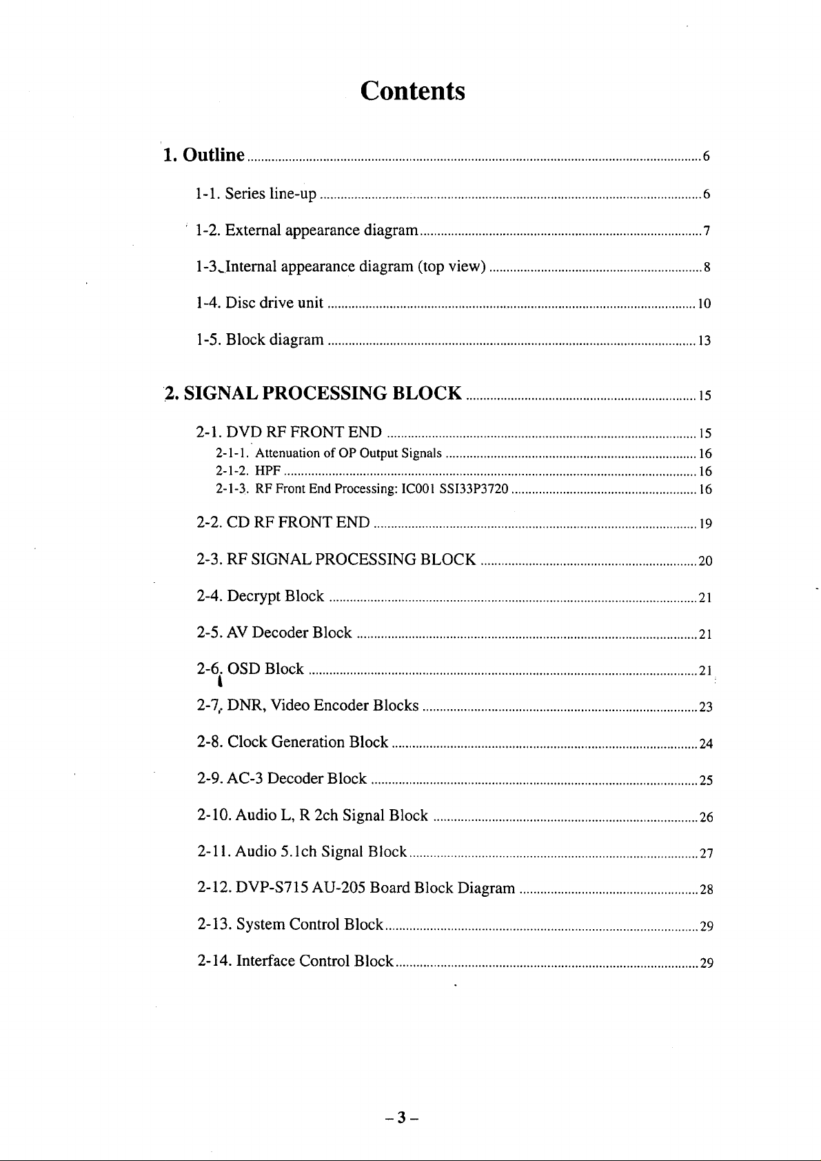
1. Outline ....................................................................................................................................6
1-1. Series line-up ...............................................................................................................6
1-2. External appearance diagram ..................................................................................7
1-3,.Internal appearance diagram (top view) ..............................................................8
1-4. Disc drive unit ........................................................................................................... 10
1-5. Block diagram ........................................................................................................... 13
2. SIGNAL PROCESSING BLOCK ...................................................................15
2-1. DVD RF FRONT END ..........................................................................................15
2-1-1. Attenuation of OP Output Signals ......................................................................... 16
2-1-2. HPF ........................................................................................................................ 16
2-1-3. RF Front End Processing: IC001 SSI33P3720 ...................................................... 16
2-2. CD RF FRONT END ..............................................................................................19
2-3. RF SIGNAL PROCESSING BLOCK ...............................................................2O
2-4. Decrypt Block ...........................................................................................................21
2-5. AV Decoder Block ...................................................................................................21
2-6. OSD Block .................................................................................................................21
L
2-7,. DNR, Video Encoder Blocks ................................................................................23
2-8. Clock Generation Block ......................................................................................... 24
2-9. AC-3 Decoder Block ...............................................................................................25
2-10. Audio L, R 2ch Signal Block .............................................................................26
2-11. Audio 5. lch Signal Block ....................................................................................27
2-12. DVP-S715 AU-205 Board Block Diagram ....................................................28
2-13. System Control Block ...........................................................................................29
2-14. Interface Control Block ........................................................................................29
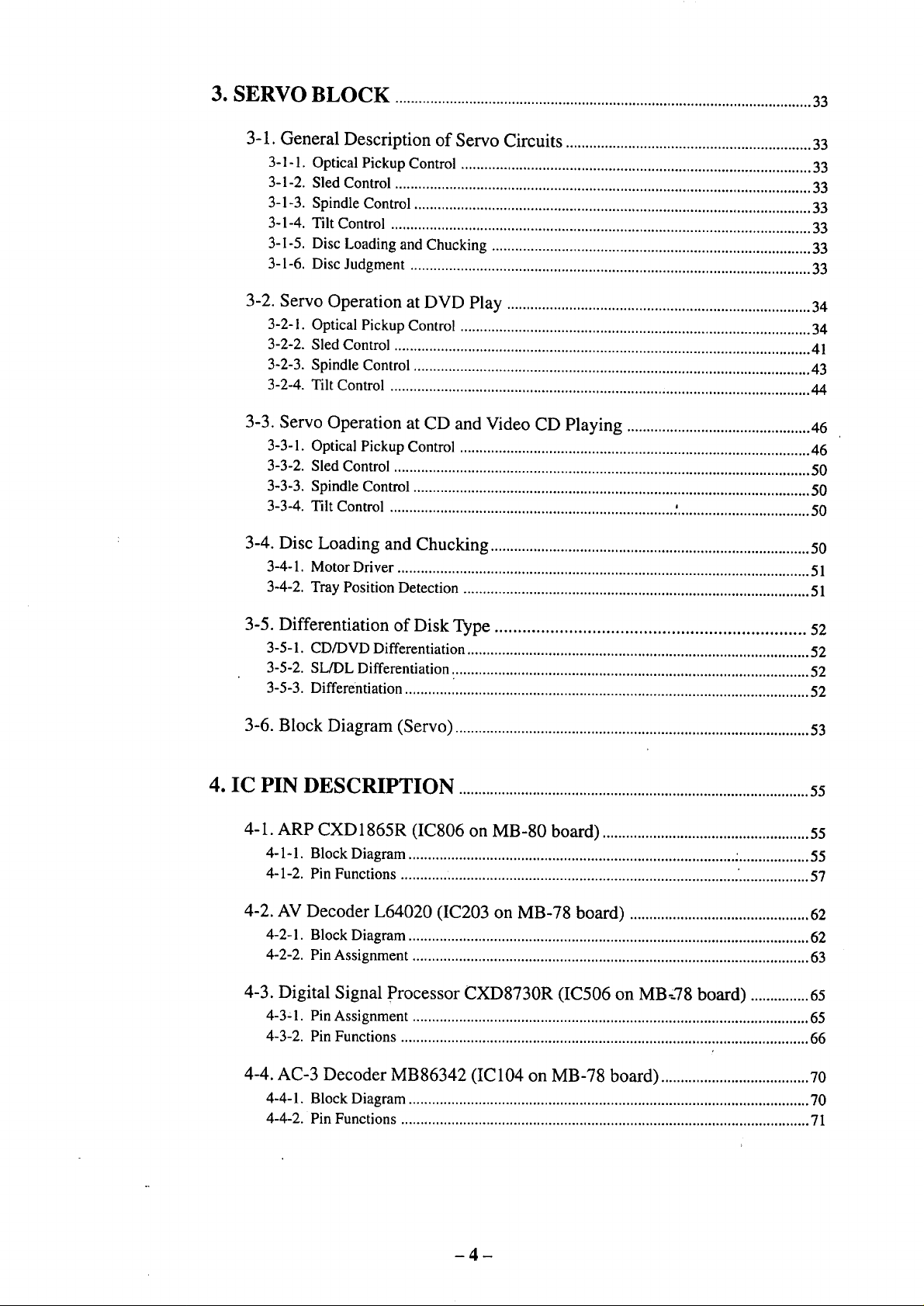
3. SERVO BLOCK ...........................................................................................................33
3-1. General Description of Servo Circuits ...............................................................33
3-1-1. Optical Pickup Control .......................................................................................... 33
3-1-2. Sled Control ........................................................................................................... 33
3-1-3. Spindle Control ...................................................................................................... 33
3-1-4. Tilt Control ............................................................................................................ 33
3-I-5. Disc Loading and Chucking .................................................................................. 33
3-1-6. Disc Judgment ....................................................................................................... 33
3-2. Servo Operation at DVD Play .............................................................................. 34
3-2-1. Optical Pickup Control .......................................................................................... 34
3-2-2. Sled Control ........................................................................................................... 41
3-2-3. Spindle Control ...................................................................................................... 43
3-2-4. Tilt Control ............................................................................................................ 44
3-3. Servo Operation at CD and Video CD Playing ...............................................46
3-3-1. Optical Pickup Control .......................................................................................... 46
3-3-2. Sled Control ........................................................................................................... 50
3-3-3. Spindle Control ...................................................................................................... 50
3-3-4. Tilt Control ......................................................................... :.................................. 50
3-4. Disc Loading and Chucking ..................................................................................50
3-4-1. Motor Driver .......................................................................................................... 51
3-4-2. Tray Position Detection ......................................................................................... 51
3-5. Differentiation of Disk Type ................................................................... 52
3-5-1. CD/DVD Differentiation ........................................................................................ 52
3-5-2. SL/DL Differentiation ............................................................................................ 52
3-5-3. Differentiation ............ i........................................................................................... 52
3-6. Block Diagram (Servo) ...........................................................................................53
4. IC PIN DESCRIPTION ..........................................................................................55
4-1. ARP CXD1865R (IC806 on MB-80 board) .....................................................55
4-1-1. Block Diagram .................................................................................... ................... 55
4-1-2. Pin Functions ....................................................................................... '.................. 57
4-2. AV Decoder L64020 (IC203 on MB-78 board) ..............................................62
4-2-1. Block Diagram ....................................................................................................... 62
4-2-2. Pin Assignment ...................................................................................................... 63
4-3. Digital Signal Processor CXD8730R (1C506 on MB;.78 board) ............... 65
4-3:1. Pin Assignment ...................................................................................................... 65
4-3-2. Pin Functions ......................................................................................................... 66
4-4. AC-3 Decoder MB86342 (IC104 on MB-78 board) ......................................70
4-4-1. Block Diagram ....................................................................................................... 70
4-4-2. Pin Functions ......................................................................................................... 71
-4-
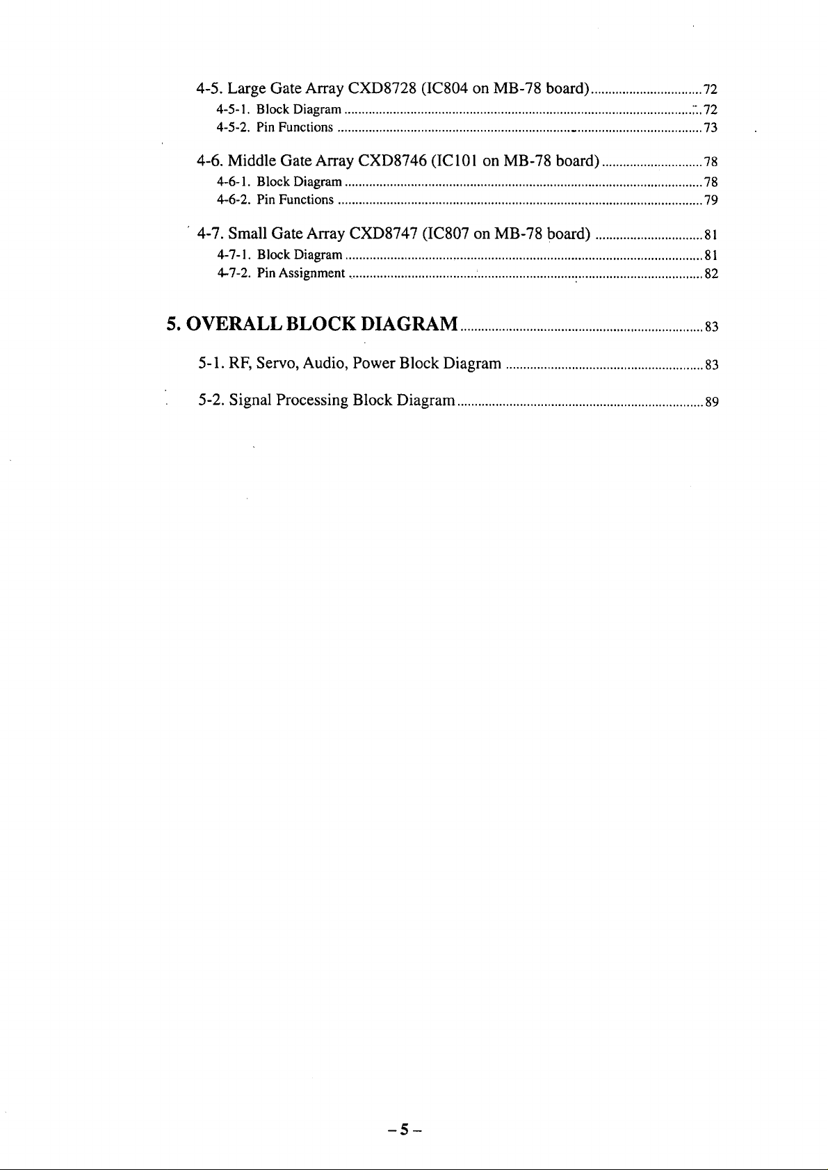
4-5. Large Gate Array CXD8728 (IC804 on MB-78 board) ................................ 72
4-5-1. Block Diagram .................................................................................................... 7..72
4-5-2. Pin Functions ........................................................................................................ 73
4-6. Middle Gate Array CXD8746 (IC 101 on MB-78 board) ............................. 78
4-6-1. Block Diagram ....................................................................................................... 78
4-6-2. Pin Functions ......................................................................................................... 79
' 4-7. Small Gate Array CXD8747 (IC807 on MB-78 board) ............................... 81
4-7-1. Block Diagram ....................................................................................................... 81
4-7-2. Pin Assignment ..................................... ............................ :.................................... 82
5. OVERALL BLOCK DIAGRAM ......................................................................83
5-1. RF, Servo, Audio, Power Block Diagram ......................................................... 83
5-2. Signal Processing Block Diagram ....................................................................... 89
5
1. Outline
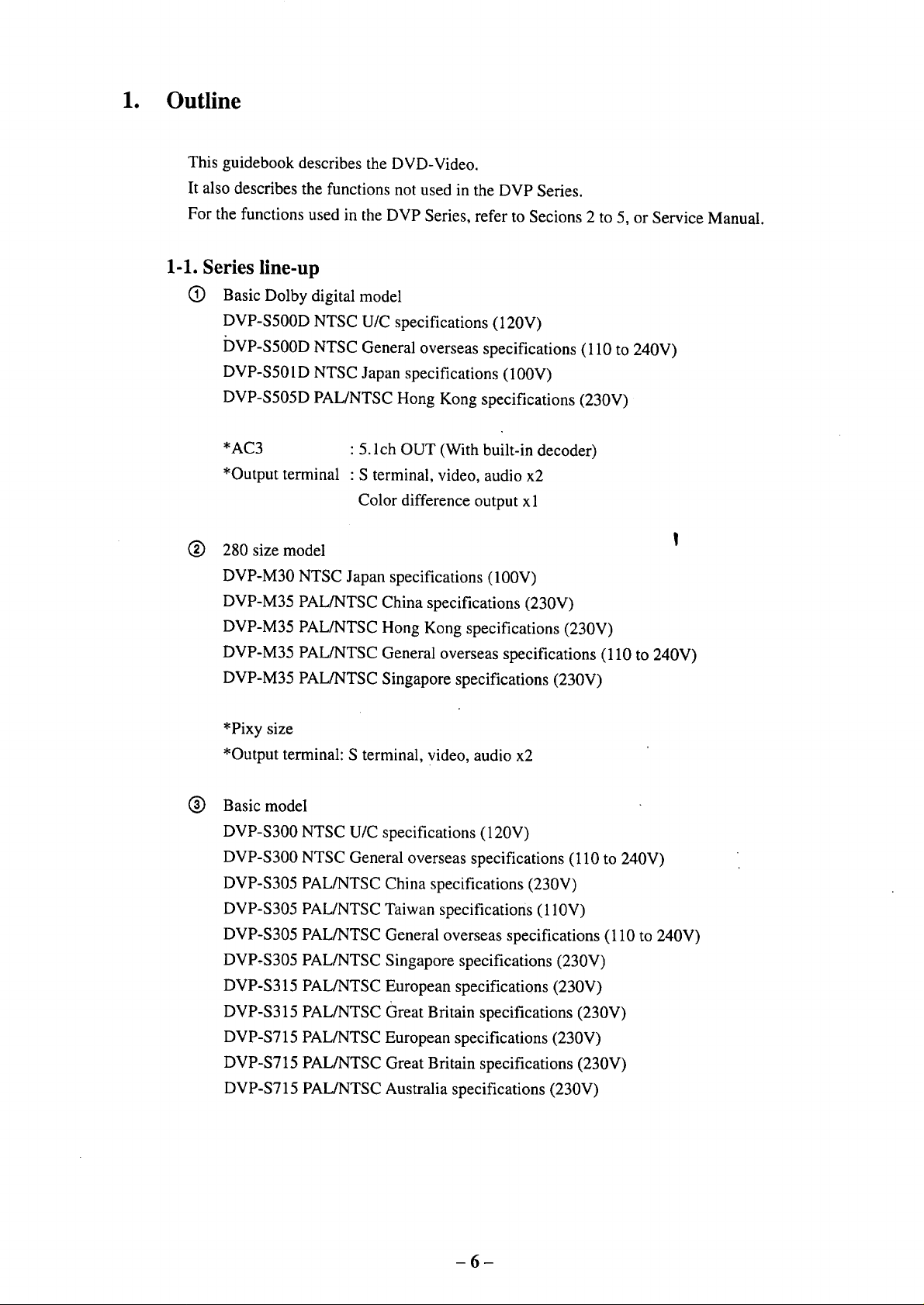
This guidebook describes the DVD-Video.
It also describes the functions not used in the DVP Series.
For the functions used in the DVP Series, refer to Secions 2 to 5, or Service Manual.
1-1. Series line-up
O Basic Dolby digital model
DVP-S500D NTSC U/C specifications (120V)
DVP-S500D NTSC General overseas specifications (110 to 240V)
DVP-S501D NTSC Japan specifications (100V)
DVP-S505D PAL/NTSC Hong Kong specifications (230V)
*AC3
*Output terminal
®
280 size model
DVP-M30 NTSC Japan specifications (100V)
DVP-M35 PAL/NTSC China specifications (230V)
DVP-M35 PAL/NTSC Hong Kong specifications (230V)
DVP-M35 PAL/NTSC General overseas specifications (110 to 240V)
DVP-M35 PAL/NTSC Singapore specifications (230V)
*Pixy size
*Output terminal: S terminal, video, audio x2
®
Basic model
DVP-S300 NTSC U/C specifications (120V)
DVP-S300 NTSC General overseas specifications (110 to 240V)
DVP-S305 PAL/NTSC China specifications (230V)
DVP-S305 PAL/NTSC Taiwan specifications (ll0V)
DVP-S305 PAL/NTSC General overseas specifications (110 to 240V)
DVP,S305 PAL/NTSC
DVP- $315 PAL/NTSC
DVP-S315 PAL/NTSC
DVP-S715 PAL/NTSC
DVP-S715 PAL/NTSC Great Britain specifications (230V)
DVP-S715 PAL/NTSC Australia specifications (230V)
: 5.1 ch OUT (With built-in decoder)
: S terminal, video, audio x2
Color difference output xl
Singapore specifications (230¥)
European specifications (230V)
Great Britain specifications (230V)
European specifications (230V)
-6-
*Output terminal
Note: Video-CDs recorded in the PAL format can be played only by general overseas
specifications models.
AC3
21P Euro (DVP-S315, $715)
S terminal, video, audio x l
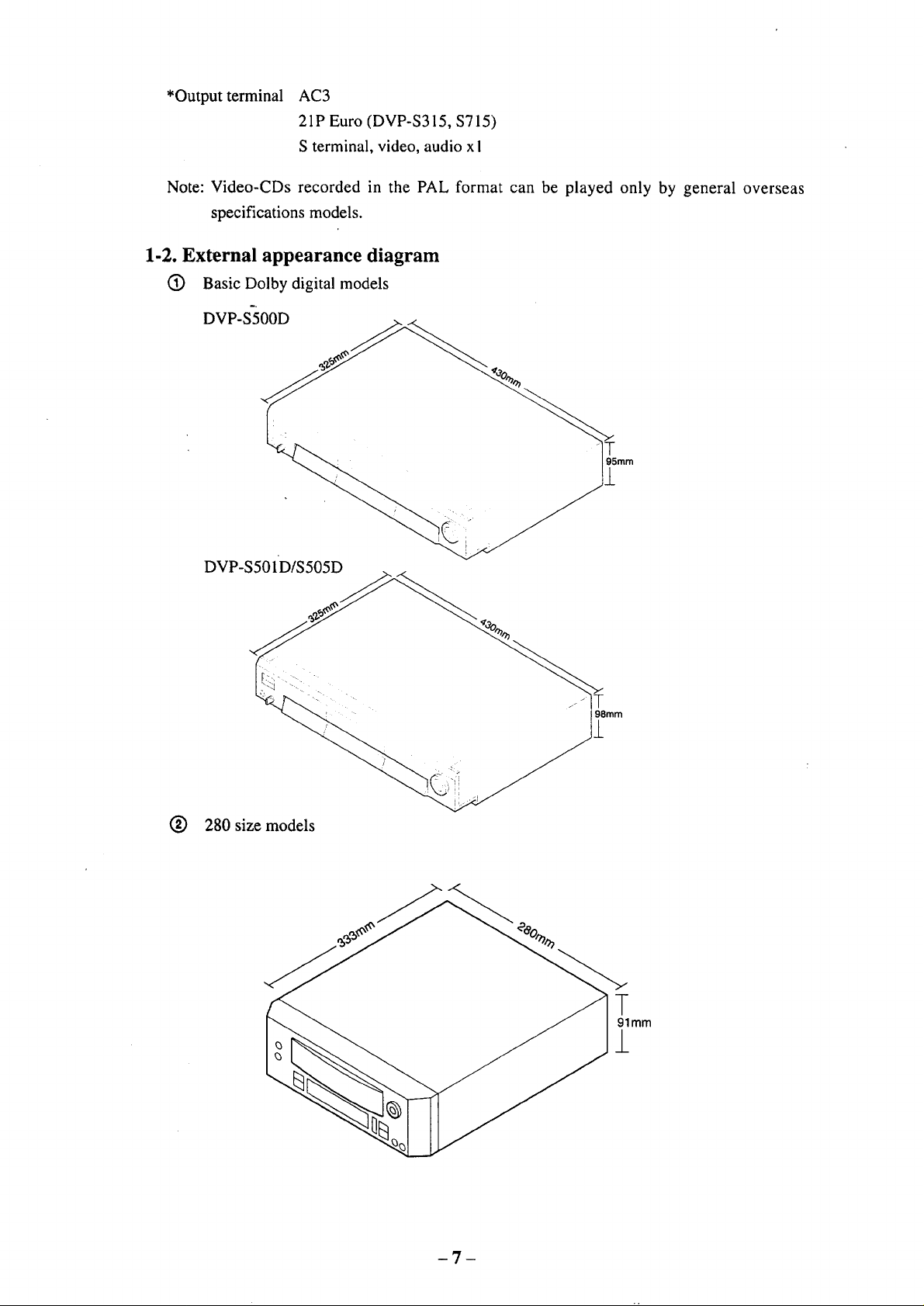
1-2. External appearance diagram
(_) Basic Dolby digital models
DVP-S'500D
DVP-S501D/S505D
(_) 280 size models
98ram
±
T
91mm
1
7
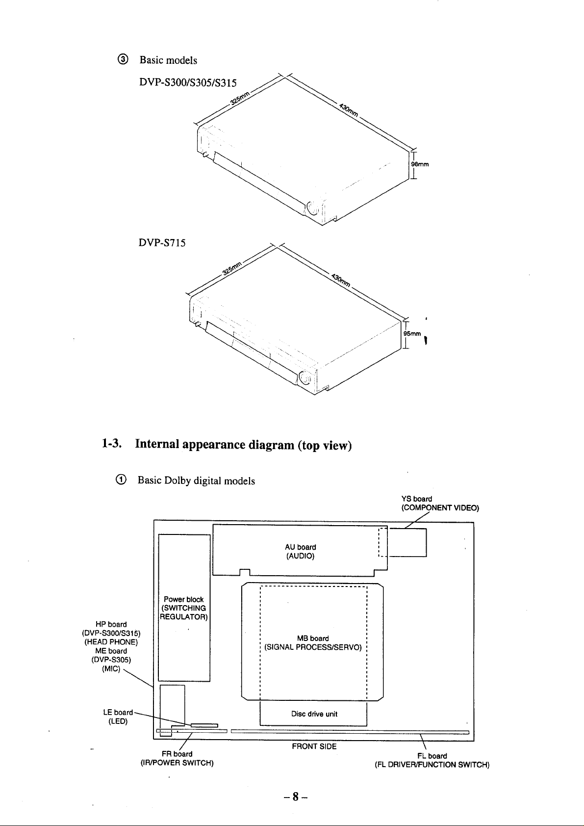
(_ Basic models
DVP-S300/S305/S315
DVP-S715
±
i
!
1-3. Internal appearance diagram (top view)
(_) Basic Dolby digital models
AU board
(AUDIO)
.__.__F3
.........................
I
MB board
(SIGNAL PROCESS/SERVO)
i
Disc drive unit
FRONT SIDE
HP board
(DVP-S300/S315)
(HEAD PHONE)
ME board
(DVP-S305)
(MIC)
LE board
(LED)
Power block
(SWITCHING
REGULATOR
';---; ' /
/
FR board
(IR/POWER SWITCH)
YS board
(COMPONENT VIDEO)
J
i
1
i
\
FL board
(FL DRIVER/FUNCTION SWITCH)
8

(_) 280 size models
POWER BLOCK _..
FL board
--....,
\
LE board
MB-board
I o,sco ,vou , i
I I
/
FRONT SIDE
, , '1
i i
j AU-board
j HP board
/
(HEAD PHONE)
(_) Basic models
HP board
(HEAD PHO._
PS board (DVP-S715) Power transformer AU board
Power
block
(SWITCHING
REGULATOR)
(AUDIO POWER) (DVP-S715) ,_ (AUDIO)
............. .......... _tIII tIIII111lIlllll_I ........ JI111 _ Iltl""IIll "
MB board
(SIGNAL PROCESS
/SERVO)
Disc drive unit
ER board
(DVP-S315/S715)
(EURO AV)
iii f --J I
' ' /
/
FL board
(IR/POWER SWITCH)
FRONT SIDE
FL board
(FL DRIVEFVFRUNCTION SWITCH)
9
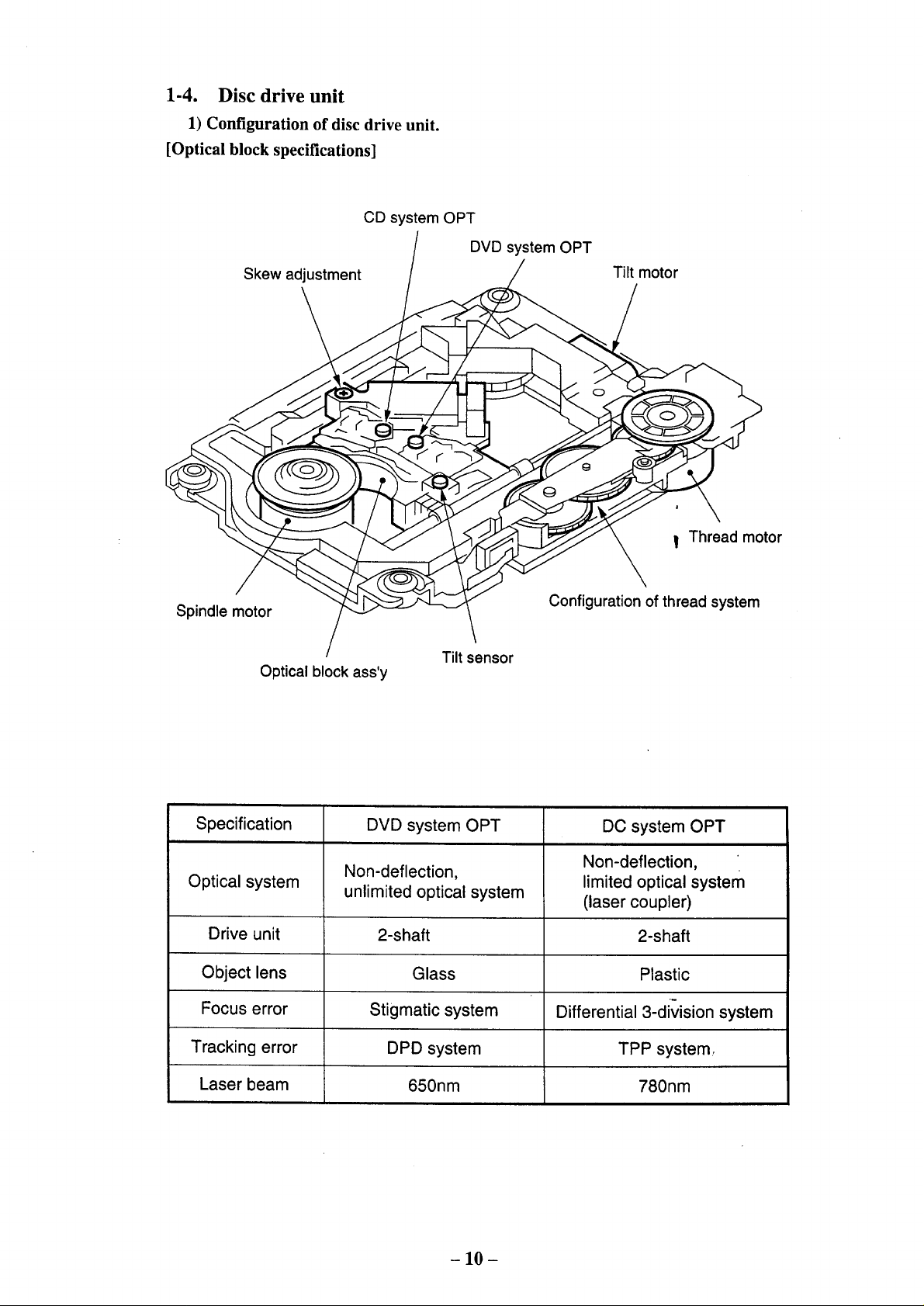
1-4. Disc drive unit
1) Configuration of disc drive unit.
[Optical block specifications]
CD system OPT
Skew adjustment
J
DVD system OPT
Tilt motor
i Thread motor
Spindle motor
Tilt sensor
Optical block ass'y
Specification DVD system OPT DC system OPT
Non-deflection, limited optical system
Optical system unlimited optical system (laser coupler)
Drive unit 2-shaft 2-shaft
Object lens Glass Plastic
Focus error Stigmatic system Differential 3-division system
Tracking error DPD system TPP system,
Configuration of thread system
Non-deflection,
Laser beam 650nm 780nm
- 10-
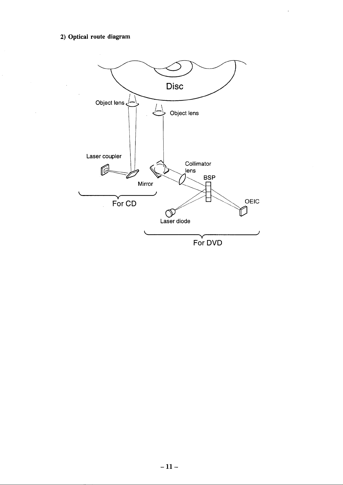
2) Optical route diagram
Las Objec ator
_.... lens
k
y J
ForCD (__ ' ' -_"_ OEIC
Mirror _)_._,._
Laser diode
Y
For DVD
-11-

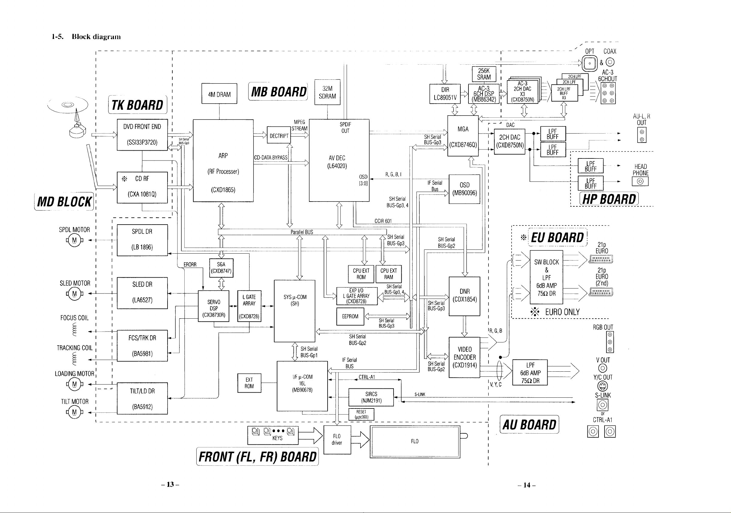
1-5. Block diagram
ITKBOARDI
©
I
SPDLMOTOR I
@ '
DVDFRONTEND
(SSI33P3720)
_. CDRF
(CXA1081Q)
I
SPDLDR
(LB1896)
/
/
AU-L,R
OUT
D
4MDRAM IMB BOARD1
MPEG
32M
SDRAM
I............ OPT COAX
.i : &(_)
256K i -_
SRAM I , i 2CHLPF AC-3
I Lc8D910R51vH (MBA8C63342)6CHDSP __l]__ _x3 2C_PFB_F___l--;__
SPDIF
OUT
...... -_ MGA ____.1 I_ _PF---_ ,..
--- -- SHSerial"l I I I 2CHDAC I T-I BUFF I r *
_-- B_(OXD8746Q)[ I_I(oxDa750N)I_I F_
ARP
(RFProcesser)
(CXD1865)
AVDEC
(L64020)
OSD_ R,G,B,I / ill / ,, --
[3:0] -- IFSerial OSD / , LP.F
SHSerial - Bus_ (MB90096) BUFf /
"-_1 _ _ rTCL_ ..........
HEAD
PHONE
OARDI
[
'i
I
ParallelBUS
Z
1411
- s_oo ,4I '11,
CCIR601 ___ I I _ l[ '- .... .-_------ -------------- -----T - - -
__SHSeri_ SHSerial !1 ÷ EU BOARD
AI IIBUS-Gp'_BUS-ep2_ ,.................... P 21p
SLEDMOTOR
@. ,
FOCUSCOIL I
_ ,
TRACKINGCOIL
LOADINGMOTOR
_ I- - ""
I
TILTMOTOR I
®,
t
I
I
I
i
i
SLEDDR
(LA6527)
FCS!FRKDR
(BA5981)
1
TILT/LDDR l" "_
(BA5912)
1
ERORR
SGAI
SERVO ARI
DSP
(CXD8730R)i I(C×D
H lG
I
_E
IAY
}728)
i
SYSp-COM
(SH)
SHSerialBUS-Gpl
I/Fp-COM
16L
(MB90678)
4_4_
CPRUoEMXTIICPRuAEMxT
.I EXPi-qTd--:_
LGATEARRAY
1 _(CXD8728) l_
I E_o_< ___ >
_-- SHSera
/1
BUS-Gp2
IFSerial I1<_ ENCODER I
BUS SHSerial (CXD1914)
CTRL-A1
RESETI
(ppc393) I
7-
FLO
driver
SIRCS(NJM2191)
[ZJ SWBLOCK
& 21p
I EURO
IISHSerial (CDX1854) L----J 75aDR
BUS-G"3/_ "_ EUROONLY RGBOUT
BUS-Gp2
S-LINK
'v' LPF EURO
IR,G,B
VIDEO
LPF
6dBAMP
75_ DR
__i) Y/OOUZ
- _
1,4.
FLO
U
V OUT
©
@
S-LINK
or
CTRL-A1
F_ONT(FL,FR)BOAR_
- 13- - 14 -
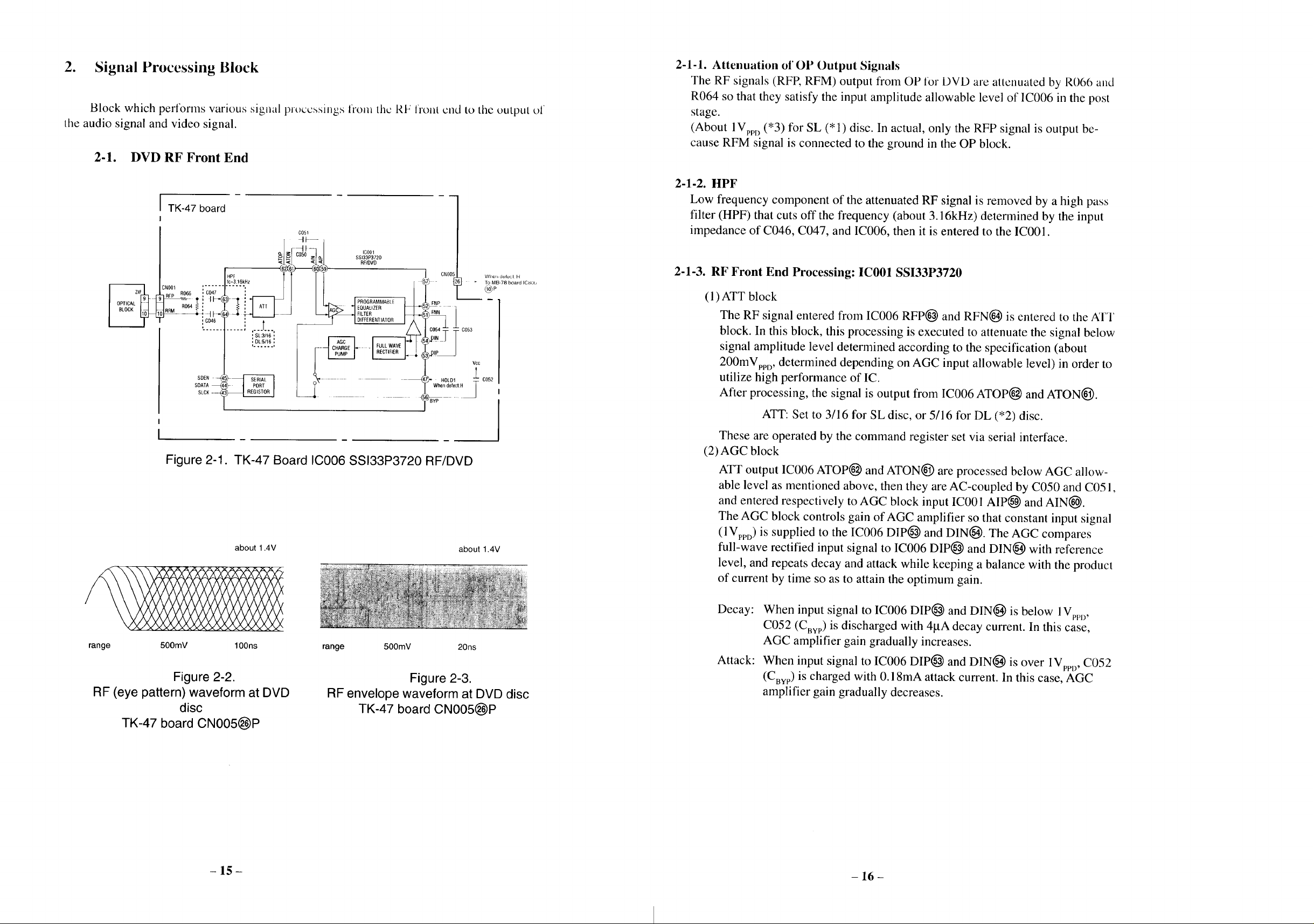
2. Signal Processing Block
Block which perfornls various signal proccssings from the RF frollt cnd to the output of
the audio signal and video signal.
2-1. DVD RF Front End
2-1-1. Attenuation of OP Output Signals
The RF signals (RFP, RFM) output from OP for DVD are attenuated by R066 and
R064 so that they satisfy the input amplitude allowable level of IC006 in the post
stage.
(About IVpp D (*'3) for SL (*1) disc. In actual, only the RFP signal is output be-
cause RFM signal is connected to the ground in the OP block.
2-1-2. ttPF
TK-47 board
0051
CR001
R066 ,0047
.ru ._ - t F_ 4)
i 0046
SDATA
SDEN --
SLCK
IC=3.16kHz
...L..
' SL:3 6
', DL:5/16 !
oo o ,coo,
_ _ _ RFIDVD
i 17171ii ,
8SI33P3720
',V_a..,,,,o0_ <"
CNO0_
_
_ _- c053
_.,.T T
]_DIP_ VCC
Figure 2-1. TK-47 Board IC006 SSI33P3720 RF/DVD
about 1.4V
When delecl H
TO MB-78 board ICs0b
about 1.4V
Low frequency component of the attenuated RF signal is removed by a high pass
filter (HPF) that cuts off the frequency (about 3.16kHz) determined by the input
impedance of C046, C047, and IC006, then it is entered to the IC001.
2-1-3. RF Front End Processing: IC001 SSI33P3720
(1) ATT block
The RF signal entered from IC006 RFP(_) and RFN(_ is entered to the ATT
block. In this block, this processing is executed to attenuate the signal below
signal amplitude level determined according to the specification (about
200mVwD, determined depending on AGC input allowable level) in order to
utilize high performance of IC.
After processing, the signal is output from IC006 ATOP_ and ATONe).
ATT: Set to 3/16 for SL disc, or 5/16 for DL (*2) disc.
These are operated by the command register set via serial interface.
(2) AGC block
ATT output IC006 ATOP(_ and ATONe) are processed below AGC allow-
able level as mentioned above, then they are AC-coupled by C050 and C051,
and entered respectively to AGC block input IC001 AIP_ and AIN(_.
The AGC block controls gain of AGC amplifier so that constant input signal
(1VppD) is supplied to the IC006 DIP@ and DIN_). The AGC compares
full-wave rectified input signal to IC006 DIP(_ and DIN(_) with reference
level, and repeats decay and attack while keeping a balance with the product
of current by time so as to attain the optimum gain.
range 500mV lO0ns range 500mV 20ns
Figure 2-2.
RF (eye pattern) waveform at DVD
disc
RF envelope waveform at DVD disc
TK-47 board CN005(_P
Figure 2-3.
TK-47 board CN005_)P
- 15 - - 16 -
Decay:
Attack:
When input signal to IC006 DIP(_ and DIN(_) is below I Vppl) ,
C052 (CByp)is discharged with 41aA decay current. In this case,
AGC amplifier gain gradually increases.
When input signal to IC006 DIP_ and DIN(_) is over 1VpeD, C052
(CuvP) is charged with 0.18mA attack current. In this case, AGC
amplifier gain gradually decreases.
Theinputsignalto IC006DIP_ andDIN_) isa signalprocessedafterEQblock
mentionedlater.
"1:SingleLayerdisc *2:DualLayerdisc *3:PeaktoPeakDifferential
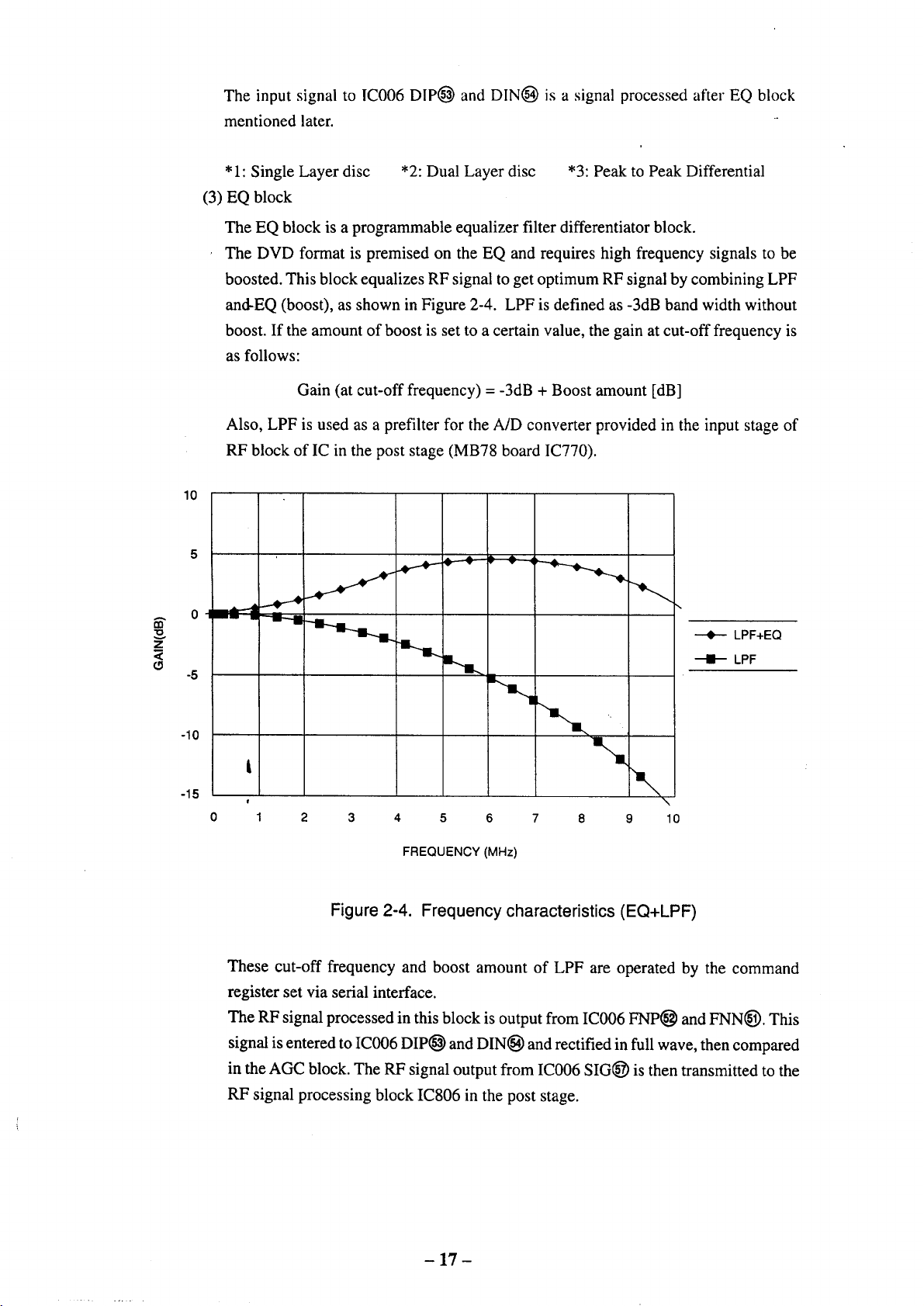
(3)EQblock
TheEQblockisaprogrammableequalizerfilterdifferentiatorblock.
TheDVDformatis premisedontheEQandrequireshighfrequencysignalstobe
boosted.ThisblockequalizesRFsignaltogetoptimumRFsignalbycombiningLPF
and-EQ(boost),asshowninFigure2-4.LPFisdefinedas-3dBbandwidthwithout
boost.If theamountofboostissettoacertainvalue,thegainatcut-offfrequencyis
asfollows:
Gain(atcut-offfrequency)=-3dB+Boostamount[dB]
Also,LPFisusedasaprefilterfortheA/Dconverterprovidedintheinputstageof
RFblockofICinthepoststage(MB78boardIC770).
10
v
_z
wl
-5
-10
-15
t
0
1 2 3 4 5 6 7 8 9 10
FREQUENCY (MHz)
Figure 2-4. Frequency characteristics (EQ+LPF)
These cut-off frequency and boost amount of LPF are operated by the command
register set via serial interface.
The RF signal processed in this block is output from IC006 FNP_ and FNN(_). This
signal is entered to IC006 DIP_ and DIN(_) and rectified in full wave, then compared
in the AGC block. The RF signal output from IC006 SIG(_ is then transmitted to the
RF signal processing block IC806 in the post stage.
---e.--- LPF+EQ
--D-- LPF
- 17 -
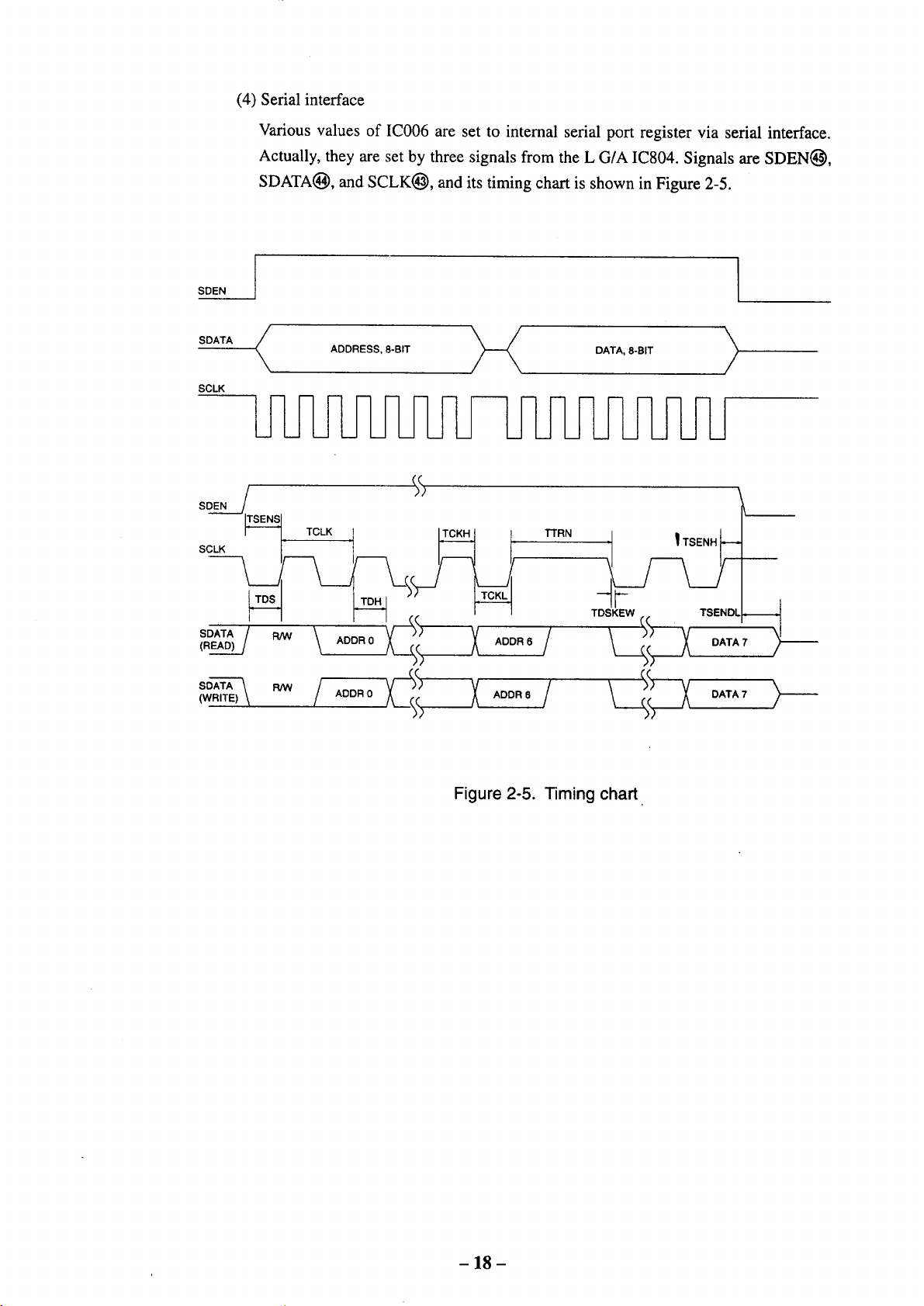
(4) Serial interface
Various values of IC006 are set to internal serial port register via serial interface.
Actually, they are set by three signals from the L G/A IC804. Signals are SDEN_,
SDATA_), and SCLK(_, and its timing chart is shown in Figure 2-5.
SDEN
SDATA (
SCLK
SDEN
SCLK
SDATA /
(READ)/
SDATA \
(WRITE)
LJ
ADDRESS, 8-BIT _ DATA, 8-BIT
TCLK TTRN
ADDR0
ADDR0
Figure 2-5. Timing chart
)
- 18-
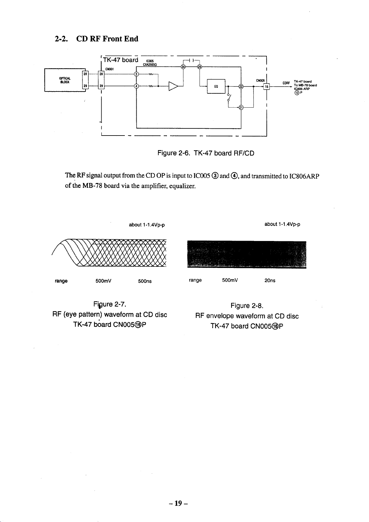
2-2. CD RF Front End
rTK-47 board
CXA,?.5550
OPTICAL
BLOCK
_1 cNO01 -_
<
CDRF TK-47 board
To MB-78 board
IC.806 ARP
Figure 2-6. TK-47 board RF/CD
The RF signal output from the CD OP is input to IC005 (_) and (_), and transmitted to IC806ARP
of the MB-78 board via the amplifier, equalizer.
about 1-1.4Vp-p
about 1-1.4Vp-p
range 500mY 500ns range 500mY 20ns
Fi0ure 2-7.
RF (eye pattern) waveform at CD disc
I
TK-47 board CN005(_P
RF envelope waveform at CD disc
TK-47 board CN005(_P
Figure 2-8.
- 19 -

2-3. RF Signal Processing Block
The block is composed of the IC806 ARP (CXD 1865R) and IC810 4Mbit DRAM (I.tPD424260)
of the MB-78 board.
In the case of the DVD, the ARP is input with the AGC and RF equalize-processed DVD-RF
signal at the IC006 analog front end (SSI33P3720) of the TK-47 board. In the case of the CD-
DA and video-CD, it is input with the CD-RF signal from IC005 of the TK-47 board.
In the ARP, first RF signal processing such as asymmetry correction, adaptive equalization, and
sync clock extraction by the RF-PLL are carried out so that the signal becomes binary data
synchronized with the PLL clock. This data is EFMPlus demodulated (DVD)/EFM demodulated
(CD-DA and video-CD) in the demodulator, subjected to frame/sector sync detection, address
detection, and protection, and sent to the buffer memory controller.
In the case of the DVD and video-CD, the ARP is linked to the ECC core, built-in and external
memories, and output controller to carry out error correction, descrambling, EDC detection,
navigation information detection (DVD only), and output data flow control, etc. The data output
in this way is then sent to the decrypt block in the next stage.
This is the same for the CDDA. The ARP is linked to the built-in and external memories, and
CDDA signal processing block to carry out error correction, output datll flow control, etc. The
signal is then muted and corrected by the CDDA signal processing block, and then sent to the
IC203AV decoder (L64020).
For all of these disks, RF jitter is calculated by the RF signal processing block, and this
information is used for adaptive control of the servo DSP via the CPU.
J
DVD-RF (
From TK-47 boa_
From TK-47 boa_
CD-RF.(
ARP DECRYPT
IC806
CXD1865R
_O LRCK (. To AV decoder IC203
CD DATA) _J, _-.-, ,_J, _-._
MDO-15 MAO-8
IC810
4M DRAM
pPD424260
IC811
CXD1904G
OCRSD0 - 7
TOS
ERROR
AVALID
DCK
AREQ
'To AV decoder IC203
Figure 2-9. MB-78 board RF processor, decrypt
- 20 -
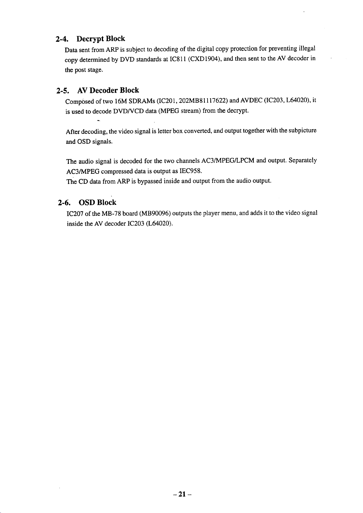
2-4. Decrypt Block
Data sent from ARP is subject to decoding of the digital copy protection for preventing illegal
copy determined by DVD standards at ICS11 (CXD1904), and then sent to the AV decoder in
the post stage.
2-5. AV Decoder Block
Comp0sed of two 16M SDRAMs (IC201,202MB 81117622) and AVDEC (IC203, L64020), it
is used to decode DVD/VCD data (MPEG stream) from the decrypt.
After decoding, the video signal is letter box converted, and output together with the subpicture
and OSD signals.
The audio signal is decoded for the two channels AC3/MPEG/LPCM and output. Separately
AC3/MPEG compressed data is output as IEC958.
The CD data from ARP is bypassed inside and output from the audio output.
2-6. OSD Block
IC207 of the MB-78 board (MB90096) outputs the player menu, and adds it to the video signal
inside the AV decoder IC203 (L64020).
- 21 -
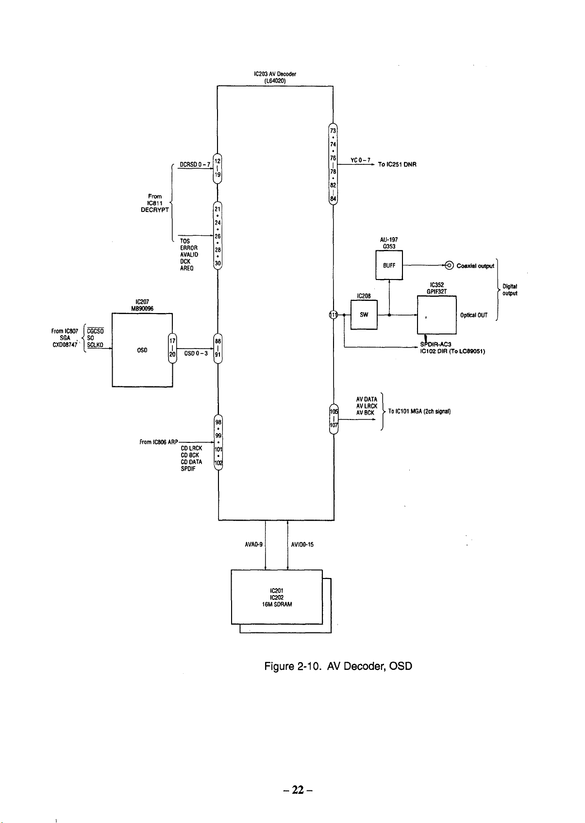
IC203 AV Decoder
(L64020)
FromIC807 ('CG--'_'O
SGA , _SO
CXD08747 ' L SCLKO
DCRSD 0-7
TOS
ERROR
AVALID
DCK
AREQ
IC207
MB90096
OSO
FromIC806ARP --
CDLRCK
CDBCK
CDDATA
SPDIF
YC0-7
-- To IC251 DNR
AU-197
0353
AVDATA
AV LRCK
AVBCK
t To IC101 MGA (2cll signal)
iC351_ C°axial °utptzt ] 0joltal
GPIF32T I output
IC102 OIR (To LC8905t)
AVIO0-15
IC201
IC202
16M SOP,AM
Figure 2-10. AV Decoder, OSD
- 22 -
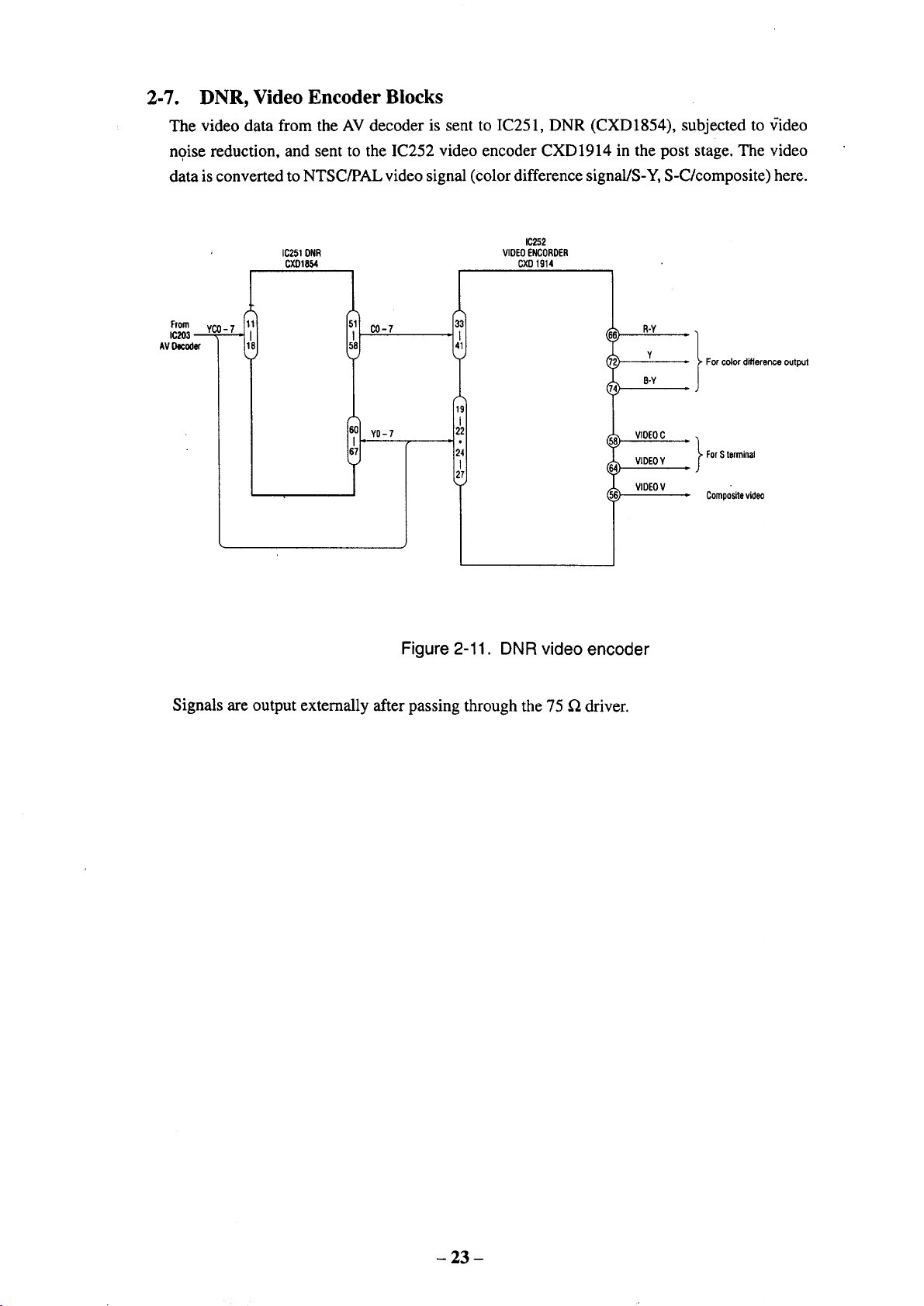
2-7. DNR, Video Encoder Blocks
The video data from the AV decoder is sent to IC251, DNR (CXD1854), subjected to video
noise reduction, and sent to the IC252 video encoder CXD1914 in the post stage. The video
data is converted to NTSC/PAL video signal (Color difference signal/S-Y, S-C/composite) here.
From vr
IC203 '"
AV Decoder
IC2510NR VIDEO ENCORDER
CXD1854 CXD 1914
C0-7
YO-7
IC252
Figure 2-11. DNR video encoder
R-Y
Y
B-Y
VIDEOC
VIDEOY
VIDEOV Compositevideo
1
For color difference output
J
ForS terminal
Signals are output externally after passing through the 75 _ driver.
- 23 -
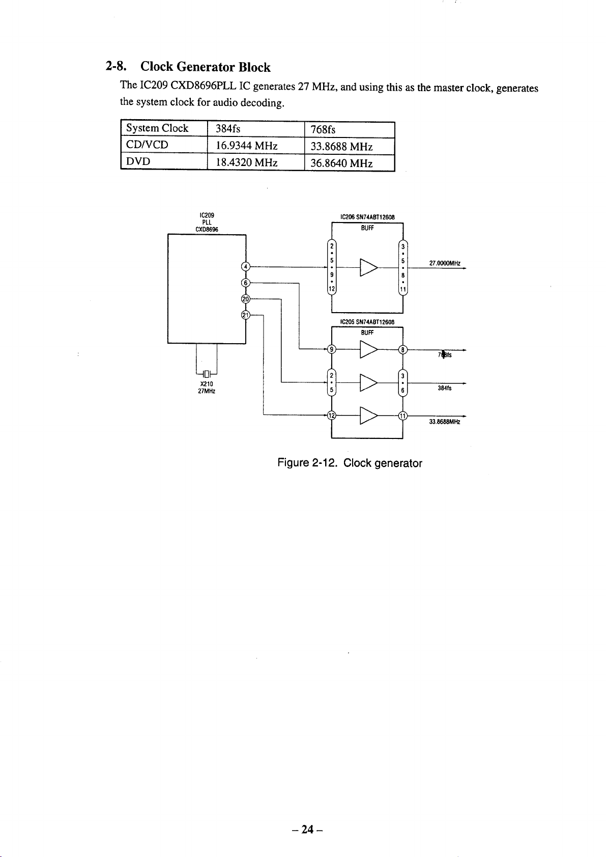
2-8. Clock Generator Block
The IC209 CXD8696PLL IC generates 27 MHz, and using this as the master clock, generates
the system clock for audio decoding.
System Clock 384fs 768fs
CD/VCD 16.9344 MHz 33.8688 MHz
DVD 18.4320 MHz 36.8640 MHz
IC209 IC206 SN74ABT12608
PLL
CXD8696 BUFF
X210
27MHz
)
27.0000MHz
)
1(;205 SN74ABT12608
BUFF
) 7_Sfs
384fs
33.8688MHz
Figure 2-12. Clock generator
=
- 24 -
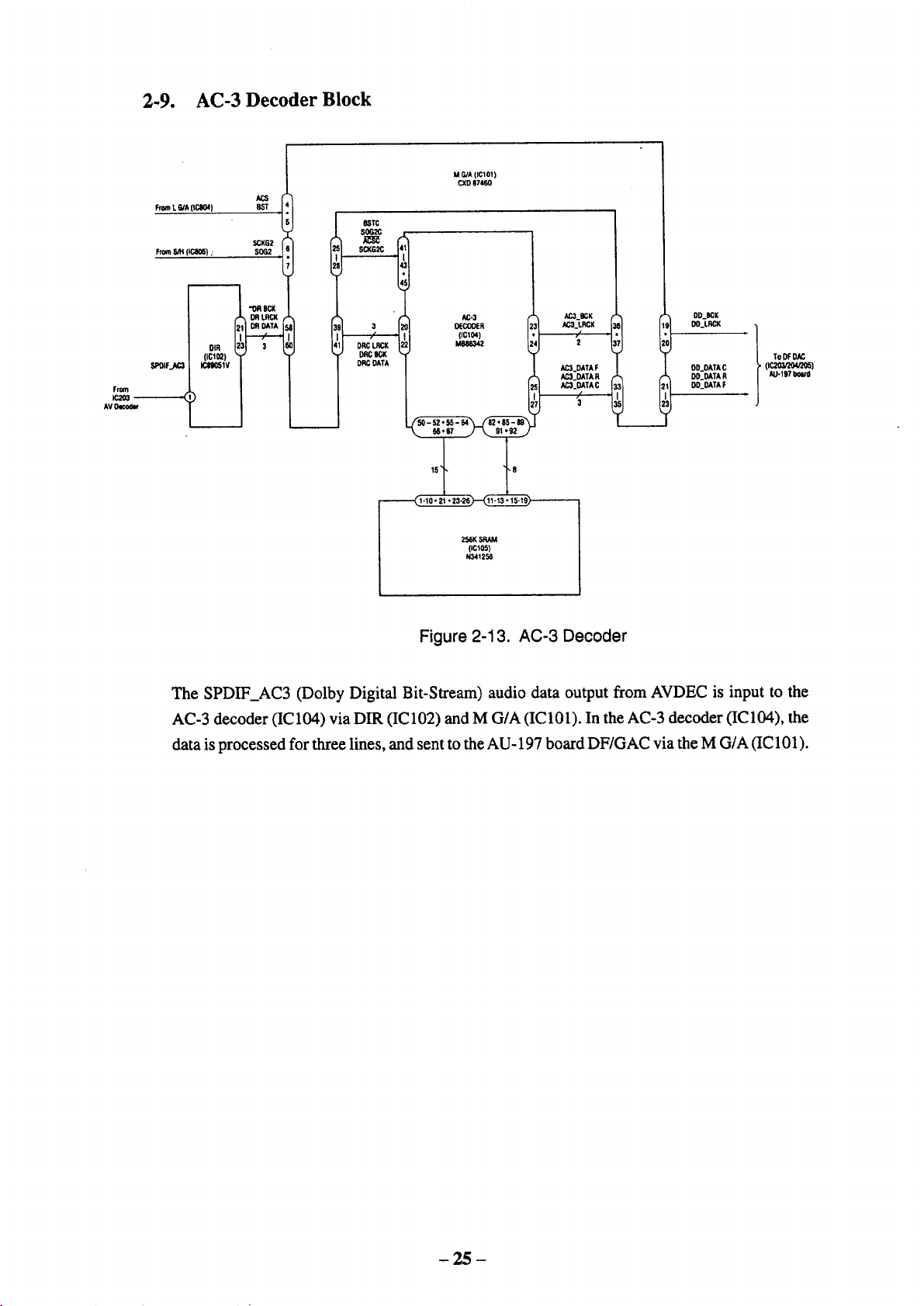
2-9. AC-3 Decoder Block
FromL_A (tC_4) 8s'r
SCKG2
SOG2From_ 11c8o5);
6STC
$062C
M G/A (IC101)
CXO 87460
AV_ II
The SPDIF_AC3 (Dolby Digital Bit-Stream) audio data output from AVDEC is input to the
AC-3 decoder (IC104) via DIR (IC102) and M G/A (IC101). In the AC-3 decoder (IC104), the
data is processed for three lines, and sent to the AU- 197 board DF/GAC via the M G/A (IC 101).
I
OR LRCK (
AC-3
DECODER
(IC_04)
M886342
256KS_
N341256
AC3__K
AC;_LRCK
/
2
AC3_DATAF
AC3_OATAR
AC3.OATA C
/
3
Figure 2-13. AC-3 Decoder
DO_LRCK
DD_BCK l
DD_OATAF 1
- 25 -
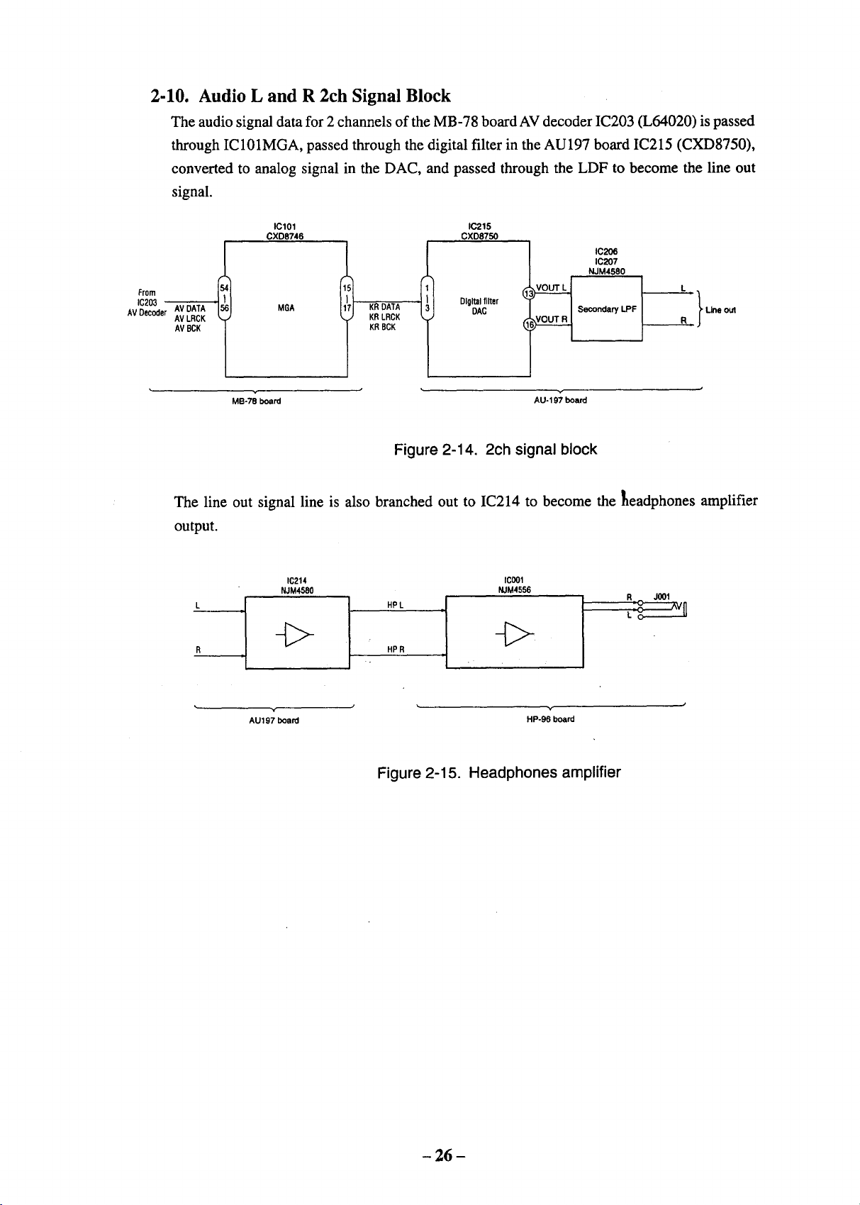
2-10. Audio L and R 2ch Signal Block
The audio signal data for 2 channels of the MB-78 board AV decoder IC203 (L64020) is passed
through IC101MGA, passed through the digital filter in the AU197 board IC215 (CXD8750),
converted to analog signal in the DAC, and passed through the LDF to become the line out
signal.
IC101 IC215
CXD8746 CXD8750
From
IC203
AVDecoder AVDATA
AVLRCK
AVBCK
The line out signal line is also branched out to IC214 to become the _eadphones amplifier
MB-78 board ""AU-197 board
MGA KRDATA
KRLRCK
KR BCK
Digitalfilter
DAC
Secondary LPF Line oul
Figure 2-14. 2ch signal block
IC206
IC207
NJM4580
output.
L
R
IC214 IC001
NJM4580 NJM4556
-E> .,. -E>
Y
AU197 board
Figure 2-15. Headphones amplifier
_r
HP-96 board
R JO01
- 26 -
2-11. Audio 5.1ch Signal Block
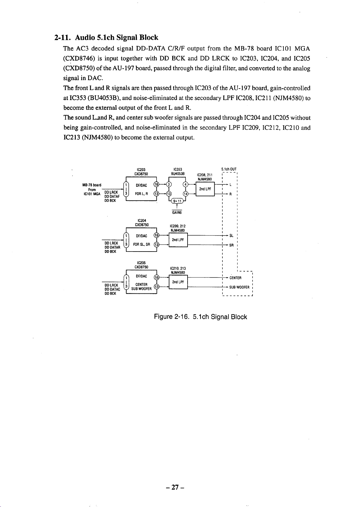
The AC3 decoded signal DD-DATA C/R/F output from the MB-78 board IC101 MGA
(CXD8746) is input together with DD BCK and DD LRCK to IC203, IC204, and IC205
(CXD8750) of the AU-197 board, passed through the digital filter, and converted to the analog
signal in DAC.
The front L and R signals are then passed through IC203 of the AU- 197 board, gain-controlled
at IC353 (BU4053B), and noise-eliminated at the secondary LPF IC208, IC211 (NJM4580) to
become the external output of the front L and R.
The sound Land R, and center sub woofer signals are passed through IC204 and IC205 without
being gain-controlled, and noise-eliminated in the secondary LPF IC209, IC212, IC210 and
IC213 (NJM4580) to become the external output.
IC203 5.1ch OUT
CXD8750
From DDLRCK = FOR L,R
MB-78board _ DF/DAC
IC101MGA DDbATAF
DDBCK
IC204
CXD8750
DD LRCK FOR SL, SR
, _ DF/DAC
DO DATAR
DO BCK
IC205
CXD8750
DD LRCK CENTER
___ DF/DAC
DD DATAC SUB WOOFER
DO 8CK
IC353
BU4053B IC208, 211
---L
_R
GAIN6
IC209,212
, - SL- SR
IC210,213
_CENTER:
' SUBWOOFER I
I I
I
Figure 2-16. 5.1ch Signal Block
I
I
_J
- 27 -
 Loading...