

Page 1
DVP-PQ2
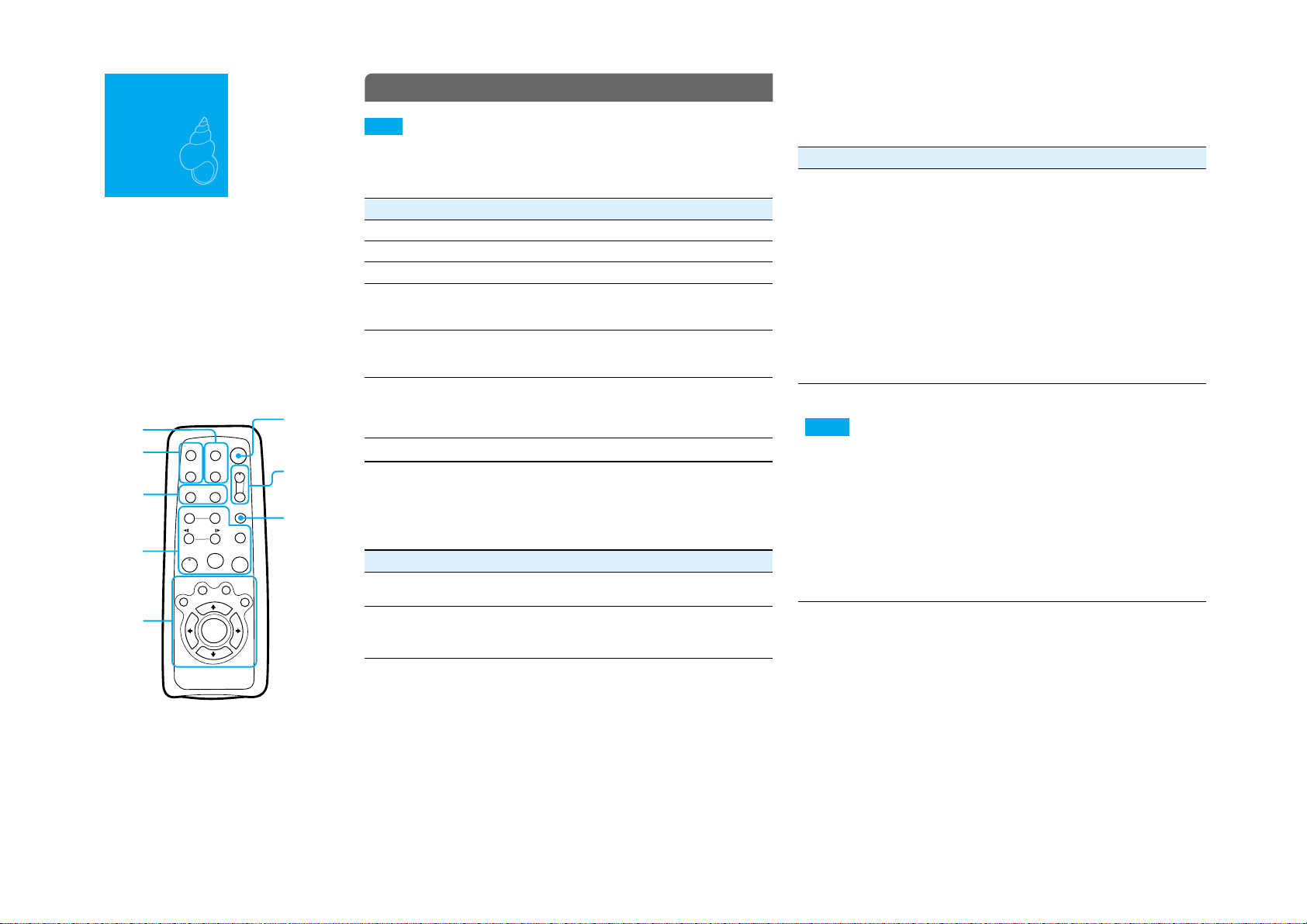
RMT-D148A
SERVICE MANUAL
SPECIFICATIONS
System
Laser: Semiconductor laser
Signal format system:
*(PQ2: MX2,U2,CA2): NTSC
*(PQ2:EC1,EC2,CEK): PAL/NTSC
Outputs
(Jack name: Jack type/Output level/Load impedance)
AUDIO OUT L/R: Phonojack/2 Vrms/10 kW
DIGITAL OUT (COAXIAL): Phonojack/0.5 Vp-p/75W
VIDEO OUT: Phonojack/1.0 Vp-p/75W
S-VIDEO OUT: 4-pin mini DIN/
Y: 1.0 Vp-p
C: 0.3 Vp-p (PAL), 0.286 Vp-p (NTSC)/75W
HEADPHONES/EARPHONES JACK:
Stereo mini-jack/9 m W + 9 m W/32W
General
Power requirements:
*(PQ2: MX2,U2,CA2): 120 V, 60 Hz
*(PQ2:EC1,EC2,CEK): 220-240 V, 50/60 Hz
Power consumption: 9 W
Dimensions (approx.): 190 ´ 147 ´ 235 mm (7 ´ 5 7/8 ´ 9 in.)
(w/h/d)
Mass (approx.): 1.3 kg (2.9 lbs)
Operating temperature: 5°C to 35°C (41°F to 95°F)
Operating humidity: 25-80%
US Model
Canada Model
Europe Model
Mexico Model
Supplied accessories
Operating Instructions (1)
Audio/video cord (1)
Remote (1)
AA (R6) size batteries (2)
EURO AV adaptor (PQ2:EC1,EC2,CEK)* (1)
Design sheet
Specifications and design are subject to change
without notice.
ENERGY STARÒ is a U.S. registered mark. As an
ENERGY STARÒ Partner, Sony Corporation has
determined that this product meets the ENERGY STAR
guidelines for energy efficiency.
* Refer Pg.4-1 for Abbreviation
Ò
CD/DVD PLAYER
Page 2

r
SAFETY CHECK-OUT
After correcting the original service problem, perform the following
safety checks before releasing the set to the customer:
1. Check the area of your repair for unsoldered or poorly-soldered connections. Check the entire board surface for solder
splashes and bridges.
2. Check the interboard wiring to ensure that no wires are
“pinched” or contact high-wattage resistors.
3. Look for unauthorized replacement parts, particularly transistors, that were installed during a previous repair. Point them
out to the customer and recommend their replacement.
4. Look for parts which, though functioning, show obvious signs
of deterioration. Point them out to the customer and recommend their replacement.
5. Check the line cord for cracks and abrasion. Recommend the
replacement of any such line cord to the customer.
6. Check the B+ voltage to see it is at the values specified.
7. Check the antenna terminals, metal trim, “metallized” knobs,
screws, and all other exposed metal parts for AC leakage.
Check leakage as described below.
: LEAD FREE MARK
Unleaded solder has the following characteristics.
• Unleaded solder melts at a temperature about 40°C higher than
ordinary solder.
Ordinary soldering irons can be used but the iron tip has to be
applied to the solder joint for a slightly longer time.
Soldering irons using a temperature regulator should be set to
about 350°C .
Caution: The printed pattern (copper foil) may peel away if the
heated tip is applied for too long, so be careful!
• Strong viscosity
Unleaded solder is more viscous (sticky, less prone to flow) than
ordinary solder so use caution not to let solder bridges occur
such as on IC pins, etc.
• Usable with ordinary solder
It is best to use only unleaded solder but unleaded solder may
also be added to ordinary solder.
LEAKAGE TEST
The AC leakage from any exposed metal part to earth ground
and from all exposed metal parts to any exposed metal part having
a return to chassis, must not exceed 0.5 mA (500 microamperes).
Leakage current can be measured by any one of three methods.
1. A commercial leakage tester, such as the Simpson 229 or RCA
WT-540A. Follow the manufacturers' instructions to use these
instruments.
2. A battery-operated AC milliammeter. The Data Precision 245
digital multimeter is suitable for this job.
3. Measuring the voltage drop across a resistor by means of a
VOM or battery-operated AC voltmeter. The “limit” indica-
tion is 0.75 V, so analog meters must have an accurate low-
voltage scale. The Simpson 250 and Sanwa SH-63Trd are ex-
amples of a passive VOM that is suitable. Nearly all battery
operated digital multimeters that have a 2 V AC range are suit-
able. (See Fig. A)
To Exposed Metal
Parts on Set
1.5 k
0.15 µF
Fig. A. Using an AC voltmeter to check AC leakage.
Ω
Earth Ground
AC
voltmete
(0.75 V)
WARNING!!
WHEN SERVICING, DO NOT APPROACH THE LASER
EXIT WITH THE EYE TOO CLOSELY. IN CASE IT IS
NECESSARY TO CONFIRM LASER BEAM EMISSION,
BE SURE TO OBSERVE FROM A DISTANCE OF
MORE THAN 25 cm FROM THE SURFACE OF THE
OBJECTIVE LENS ON THE OPTICAL PICK-UP BLOCK.
SAFETY-RELATED COMPONENT WARNING!!
COMPONENTS IDENTIFIED BY MARK OR DOTTED
LINE WITH MARK ON THE SCHEMATIC DIAGRAMS
AND IN THE PARTS LIST ARE CRITICAL TO SAFE
OPERATION. REPLACE THESE COMPONENTS WITH
SONY PARTS WHOSE PART NUMBERS APPEAR AS
SHOWN IN THIS MANUAL OR IN SUPPLEMENTS PUBLISHED BY SONY.
CAUTION:
The use of optical instrument with this product will increase eye
hazard.
CAUTION
Use of controls or adjustments or performance of procedures
other than those specified herein may result in hazardous radiation exposure.
ATTENTION AU COMPOSANT AYANT RAPPORT
À LA SÉCURITÉ!
LES COMPOSANTS IDENTIFIÉS PAR UNE MARQUE
SUR LES DIAGRAMMES SCHÉMATIQUES ET LA LISTE
DES PIÈCES SONT CRITIQUES POUR LA SÉCURITÉ
DE FONCTIONNEMENT. NE REMPLACER CES COMPOSANTS QUE PAR DES PIÈCES SONY DONT LES
NUMÉROS SONT DONNÉS DANS CE MANUEL OU
DANS LES SUPPLÉMENTS PUBLIÉS PAR SONY.
– 2 –
Page 3

TABLE OF CONTENTS
SERVICE NOTE ................................................................... 4
1. GENERAL ................................................................... 1
2. DISASSEMBLY
2-1. LID Assembly Removal ................................................. 2-1
2-2. Disk Base Assembly Removal ...................................... 2-1
2-3. Base Unit Removal ........................................................ 2-1
2-4. BU Holder Removal ....................................................... 2-1
2-5. SW-406 Board Removal ................................................ 2-2
2-6. HP-137 & Jack Plate Removal ...................................... 2-2
2-7. Lower Case Removal .................................................... 2-2
2-8. Power Switching Regulator Block Removal ................. 2-2
2-9. Shield Plate Removal .................................................... 2-3
2-10. AV-77 Board Removal ................................................... 2-3
2-11. IF-106 Board Removal .................................................. 2-3
2-12. MB-108 & SW-407 Boards Removal ............................ 2-3
2-13. Circuit Boards Location ................................................. 2-4
3. BLOCK DIAGRAMS
3-1. Overall Block Diagram ................................................... 3-1
3-2. System Control Block Diagram ..................................... 3-3
3-3. RF/Servo Block Diagram ............................................... 3-5
3-4. Signal Processor Block Diagram .................................. 3-7
3-5. Video/Audio Block Diagram .......................................... 3-9
3-6. Interface Control Block Diagram ................................... 3-11
3-7. Power 1 Block Diagram ................................................. 3-13
3-8. Power 2 Block Diagram ................................................. 3-15
4. PRINTED WIRING BOARDS AND SCHEMATIC
DIAGRAMS
5. IC PIN FUNCTION DESCRIPTION
5-1. System Control Pin Function
(MB-108 BOARD IC104: MB9130RPFV-G-BND-E1)... 5-1
6. TEST MODE
6-1. General Description ...................................................... 6-1
6-2. Starting Test Mode ......................................................... 6-1
6-3. Syscon Diagnosis .......................................................... 6-1
6-4. Drive Auto Adjustment ................................................... 6-5
6-5. Drive Manual Operation ................................................ 6-7
6-6. Emergency History ........................................................ 6-10
6-7. Version Information ....................................................... 6-11
6-8. Video Level Adjustment ................................................ 6-11
6-9. Troubleshooting ............................................................. 6-11
7. ELECTRICAL ADJUSTMENT
7-1. Power Supply Check ..................................................... 7-1
7-2. Adjustment of Video System ......................................... 7-2
1. Video Level Adjustment ................................................ 7-2
2. Checking S Video Output S-Y ....................................... 7-2
3. Checking S Video Output S-C ...................................... 7-2
7-3. Adjustment Related Parts Arrangement....................... 7-3
8. REPAIR PARTS LIST
8-1. Exploded Views ............................................................. 8-1
8-1-1. Disk Base Section .................................................... 8-1
8-1-2. Lower Case Section ................................................. 8-2
8-2. Electrical Parts List........................................................ 8-3
4-1. Printed Wiring Boards and Schematic Diagrams ........ 4-1
4-2. Frame Schematic Diagram ............................................ 4-3
Waveforms ..................................................................... 4-5
• MB-108 Printed Wiring Board .................................. 4-7
• MB-108 (System Control) Schematic Diagram ....... 4-9
• MB-108 (Motor Drive) Schematic Diagram ............. 4-11
• MB-108 (Servo) Schematic Diagram ....................... 4-13
• MB-108 (AV Decoder) Schematic Diagram ............ 4-15
• MB-108 (Audio DAC, PLL) Schematic Diagram ...... 4-17
• MB-108 Board Differential Part List ......................... 4-17
• AV-77 Printed Wiring Board ..................................... 4-19
• AV-77 (Audio/Video Out) Schematic Diagram ........ 4-21
• AV-77 Board Differential Part List............................ 4-23
• IF-106 Printed Wiring Board .................................... 4-25
• IF-106 (Interface Control) Schematic Diagram ....... 4-27
• SW-406, SW-407 Printed Wiring Boards ................ 4-29
• SW-406 (Function Switch), SW-407 (Door Switch)
Schematic Diagram ............................................. 4-31
• HP-137 Printed Wiring Board .................................. 4-33
• HP-137 (Headphone) Schematic Diagram ............. 4-35
• DPSN-20CP Printed Wiring Board .......................... 4-37
• DPSN-20CP (Switching Regulator)
Schematic Diagram ............................................. 4-39
• DPSN-20CP-2 Printed Wiring Board ....................... 4-41
• DPSN-20CP-2 (Switching Regulator)
Schematic Diagram ............................................. 4-43
– 3 –
Page 4
SERVICE NOTE
1. DISASSEMBLY
• This set can be disassembled in the order shown below.
Set
Lid Assembly
(Page 2-1)
Disk Base Assembly
(Page 2-1)
Base Unit
(Page 2-1)
BU Holder
(Page 2-1)
SW-406 Board
(Page 2-2)
HP-137 Board &
Jack Plate
(Page 2-2)
2. PRECAUTIONS FOR USE OF BASE UNIT
As the laser diode in the base unit is easily damaged by static
electricity, desolder the laser tap of the flexible board of the base
unit when using it.
Before disconnecting the connector, solder first. Before connecting the connector, be careful not to remove the solder. Also take
adequate measures to prevent damage by static electricity. Handle
the flexible board with care as it breaks easily.
Base unit
Laser tap
Lower Case
(Page 2-2)
Power Switching
Regulator Block
(Page 2-2)
Shield Plate
(Page 2-3)
AV-77 Board
(Page 2-3)
IF-106 Board
(Page 2-3)
MB-108 &
SW-407 Boards
(Page 2-3)
– 4 –
Page 5
1-1
CD/DVD Player
Operating Instructions
DVP-PQ2
Blue Side
c
c
c
Playing MP3 audio tracks
from a list
Brown Side
Playable discs and special
words
Limiting Playback
Using the Design Sheet
c
c
c
Connecting Other
Components
Precautions
3-082-452-12(1)
Connecting
the Player
Playing Discs
DVD/VIDEO CD/CD/MP3
Using the
Remote
SHUFFLE/REPEAT/AUDIO/
ANGLE/SUBTITLE/TVS
(surround)
Settings and
Adjustments
WARNING
To prevent fire or shock hazard, do not expose the
player to rain or moisture.
To avoid electrical shock, do not open the cabinet.
Refer servicing to qualified personnel only.
Power cord (mains lead) must only be changed at a
qualified service shop.
CAUTIONS
• The use of optical instruments with this product
will increase eye hazard. As the laser beam used in
this CD/DVD player is harmful to eyes, do not
attempt to disassemble the cabinet.
Refer servicing to qualified personnel only.
• TO PREVENT ELECTRIC SHOCK, MATCH WIDE
BLADE OF PLUG TO WIDE SLOT AND FULLY
INSERT.
PRECAUTIONS
• The nameplate is located at the bottom of the
player.
• To prevent fire or shock hazard, do not place
objects filled with liquids, such as vases, on the
apparatus.
For customers in the U.S.A.
Owner’s Record
The model and serial numbers are located at the
bottom of the player. Record the serial number in the
space provided below. Refer to them whenever you
call upon your Sony dealer regarding this product.
Model No. DVP-PQ2
Serial No. ___________________
You are cautioned that any change or modifications
not expressly approved in this manual could void
your authority to operate this equipment.
Note
This equipment has been tested and found to comply
with the limits for a Class B digital device, pursuant
to Part 15 of the FCC Rules. These limits are designed
to provide reasonable protection against harmful
interference in a residential installation. This
equipment generates, uses, and can radiate radio
frequency energy and if not installed and used in
accordance with the instructions, may cause harmful
interference to radio communications. However,
there is no guarantee that interference will not occur
in a particular installation. If this equipment does
cause harmful interference to radio or television
reception, which can be determined by turning the
equipment off and on, the user is encouraged to try
to correct the interference by one or more of the
following measures:
– Reorient or relocate the receiving antenna.
– Increase the separation between the equipment and
receiver.
– Connect the equipment into an outlet on a circuit
different from that to which the receiver is
connected.
– Consult the dealer or an experienced radio/TV
technician for help.
For customers in the U.S.A. and Canada
This symbol is intended to alert the user
to the presence of uninsulated
“dangerous voltage” within the
product’s enclosure that may be of
sufficient magnitude to constitute a risk
of electric shock to persons.
This symbol is intended to alert the user
to the presence of important operating
and maintenance (servicing) instructions
in the literature accompanying the
appliance.
SECTION 1
GENERAL
This section is extracted from instruction
manual (3-082-452-12(1)).
DVP-PQ2
© 2003 Sony Corporation Printed in Malaysia
Troubleshooting
Page 6
1-2
For customers in Europe
This appliance is classified as a CLASS 1 LASER
product. The CLASS 1 LASER PRODUCT
MARKING is located at the bottom of the player.
Notice for customers in the United Kingdom
and Republic of Ireland
A moulded plug complying with BS1363 is fitted to
this equipment for your safety and convenience.
Should the fuse in the plug supplied need to be
replaced, a 5 AMP fuse approved by ASTA or BSI to
BS1362, (i.e., marked with
used. If the plug supplied with this equipment has a
detachable fuse cover, be sure to attach the fuse cover
after you change the fuse. Never use the plug
without the fuse cover. If you should lose the fuse
cover, please contact your nearest Sony service
station.
or mark) must be
About this manual
Thank you for purchasing this Sony CD/DVD
Player. Before operating this player, please read this
manual thoroughly and retain it for future reference.
In this manual, the basic information on connection,
operation, and settings is given on the back side
(Blue Side). The advanced information on connection
and settings, and additional information is given on
this side (Brown Side).
Playable discs
and special
words
Identifying the discs
Playable discs
DVD VIDEOs:
VIDEO CDs:
The “DVD VIDEO” logo is a trademark.
Non-playable discs
• CD-Rs/CD-RWs/CD-ROMs (including photo
CDs) that are not in music CD or VIDEO CD
format.
• Data sections in CD-EXTRAs
• HD (high density) layer of Super Audio CDs
• DVD-ROMs, DVD Audio discs, DVD-RWs (VR
mode)
• DVDs with region codes that cannot be played on
this player.
• Irregularly shaped discs such as heart- or starshaped discs.
• A disc with stickers or glue on its surface.
For U.S./Canadian models:
• A disc recorded in a color system other than NTSC.
For European models:
• A disc recorded in the NTSC color system when
connected to a PAL TV.
• A disc recorded in the PAL color system when
connected to an NTSC TV.
Notes
• Notes about DVD-RWs/DVD-Rs, DVD+RWs/
DVD+Rs or CD-Rs/CD-RWs
Some DVD-RWs/DVD-Rs, DVD+RWs/
DVD+Rs or CD-Rs/CD-RWs cannot be played on
this player due to the recording quality or physical
condition of the disc, or the characteristics of the
recording device and authoring software.
The disc will not play if it has not been correctly
finalized. For more information, see the operating
instructions for the recording device. Note that
discs created in the Packet Write format cannot be
played.
Music CDs:
• Music discs encoded with copyright protection
technologies
This product is designed to playback discs that
conform to the Compact Disc (CD) standard.
Recently, various music discs encoded with
copyright protection technologies are marketed by
some record companies. Please be aware that
among those discs, there are some that do not
conform to the CD standard and may not be
playable by this product.
More on playable DVDs
Region code
Your player has a region code printed on the bottom
of the player (see “Precautions” for the specific
location) and will only play DVDs that are labeled
with identical region codes or the
ALL
mark.
Copyright
This product incorporates copyright protection
technology that is protected by method claims of
certain U.S. patents, other intellectual property rights
owned by Macrovision Corporation, and other rights
owners. Use of this copyright protection technology
must be authorized by Macrovision Corporation, and
is intended for home and other limited viewing uses
only unless otherwise authorized by Macrovision
Corporation. Reverse engineering or disassembly is
prohibited.
More on playable DATA CDs
Formats
You can play MP3 audio tracks recorded on CD-Rs/
CD-RWs/CD-ROMs in accordance with ISO9660*
Level1/Level2/Joliet formats.
You can also play discs with MP3 audio tracks
recorded in multisession format (a format in which
data is added on to the disc) only if an MP3 audio
track is recorded in the first session.
*A logical file format for CD-ROM formalized by the
International Organization for Standardization (ISO).
Understanding special words
Dolby* Digital
Digital audio compression technology developed by
Dolby Laboratories. Conforms to 5.1ch surround
mode.
* Manufactured under license from Dolby Laboratories. “Dolby,”
“Pro Logic,” and the double-D symbol are trademarks of Dolby
Laboratories.
DTS*
Digital audio compression technology developed by
Digital Theater Systems. Conforms to 5.1ch surround
mode.
*“DTS” and “DTS Digital Out” are trademarks of Digital Theater
Systems, Inc.
Dolby Surround (Pro Logic)
Audio signal processing technology developed by
Dolby Laboratories for surround mode.
MP3
MP3 (MPEG1 Audio Layer 3) is a standard format
defined by ISO/MPEG which compresses audio
data. This player conforms to a sampling frequency
of 32kHz, 44.1kHz, and 48kHz.
MPEG
The name of a committee that generates international
standards for the digital video and audio
compression system. Also the standard authorized
by the committee. MPEG1 conforms to up to 2channel stereo. MPEG2, used on the DVDs, conforms
to up to 7.1ch surround.
Page 7
1-3
Limiting
Playback
You can set a password and choose a playback
limitation level for DVDs with the playback
limitation function. Scenes that are limited by
this function may be blocked or replaced with
different scenes.
Setting the playback limitation
level
1
Press DISPLAY repeatedly in stop mode to
show Setup Display.
2
Select “SCREEN SETUP” using V/v, and
press ENTER.
3
Select “PARENTAL CONTROL c” using V/v,
and press ENTER.
4
Enter a 4-digit password, and press ENTER.
Select the numbers using V/v. Press b to go to
the next digit. When entering a password for
the first time, repeat this step once more to
confirm the entered password.
<TV screen>
PARENTAL CONTROL
Enter password, then press .
Enter the number starting from here.
5
Select “STANDARD” using V/v, and press
ENTER.
6
Select an area as the playback limitation
level standard (e.g., “USA”) using V/v,
and press ENTER.
When you chose “OTHERS c,” select and
enter a code number from the area code list
given at the end of this section using B/V/v/
b.
ENTER
7
Press ENTER.
8
Select the limitation level (e.g., “4:PG13”)
using V/v, and press ENTER.
The viewer limitation becomes more strict as
the number becomes lower.
To return to the previous screen
Press O.
To turn off the display
Press DISPLAY.
To change the password
After performing step 4 of “Setting the
playback limitation level,” select “CHANGE
PASSWORD c” using V/v, and press ENTER.
Enter your 4-digit password using B/V/v/b,
and press ENTER. The display for changing
the password appears. Enter a new password
and press ENTER. To confirm the password,
enter the new password again, and press
ENTER.
Playing discs with playback
limitations
1
Place the disc on the tray, and close the lid
until it clicks. Then press H.
The display for entering your password
appears.
2
Enter the 4-digit password using B/V/v/b,
and press ENTER.
Playback starts.
To cancel the playback limitation
Select “OFF” for “LEVEL” in step 8 of “Setting
the playback limitation level.”
If you forget your password
Open the lid and perform steps 1-3 of “Setting
the playback limitation level.” Enter the 6-digit
number “199703” in step 4, and press ENTER.
After entering a new password and pressing
ENTER, repeat the entire procedure from step 1
of “Playing discs with playback limitations.”
Area Code List
Standard Code number
Argentina 2044
Australia 2047
Austria 2046
Belgium 2057
Brazil 2070
Canada 2079
Chile 2090
China 2092
Denmark 2115
Finland 2165
France 2174
Germany 2109
India 2248
Indonesia 2238
Italy 2254
Japan 2276
Korea 2304
Malaysia 2363
Mexico 2362
Netherlands 2376
New Zealand 2390
Norway 2379
Pakistan 2427
Philippines 2424
Portugal 2436
Russia 2489
Singapore 2501
Spain 2149
Sweden 2499
Switzerland 2086
Thailand 2528
United Kingdom 2184
Using the
Design Sheet
You can open the clear, round-shaped cover on
the lid of this player and exchange the supplied
“design sheet” with your favorite pictures or
photos.
1
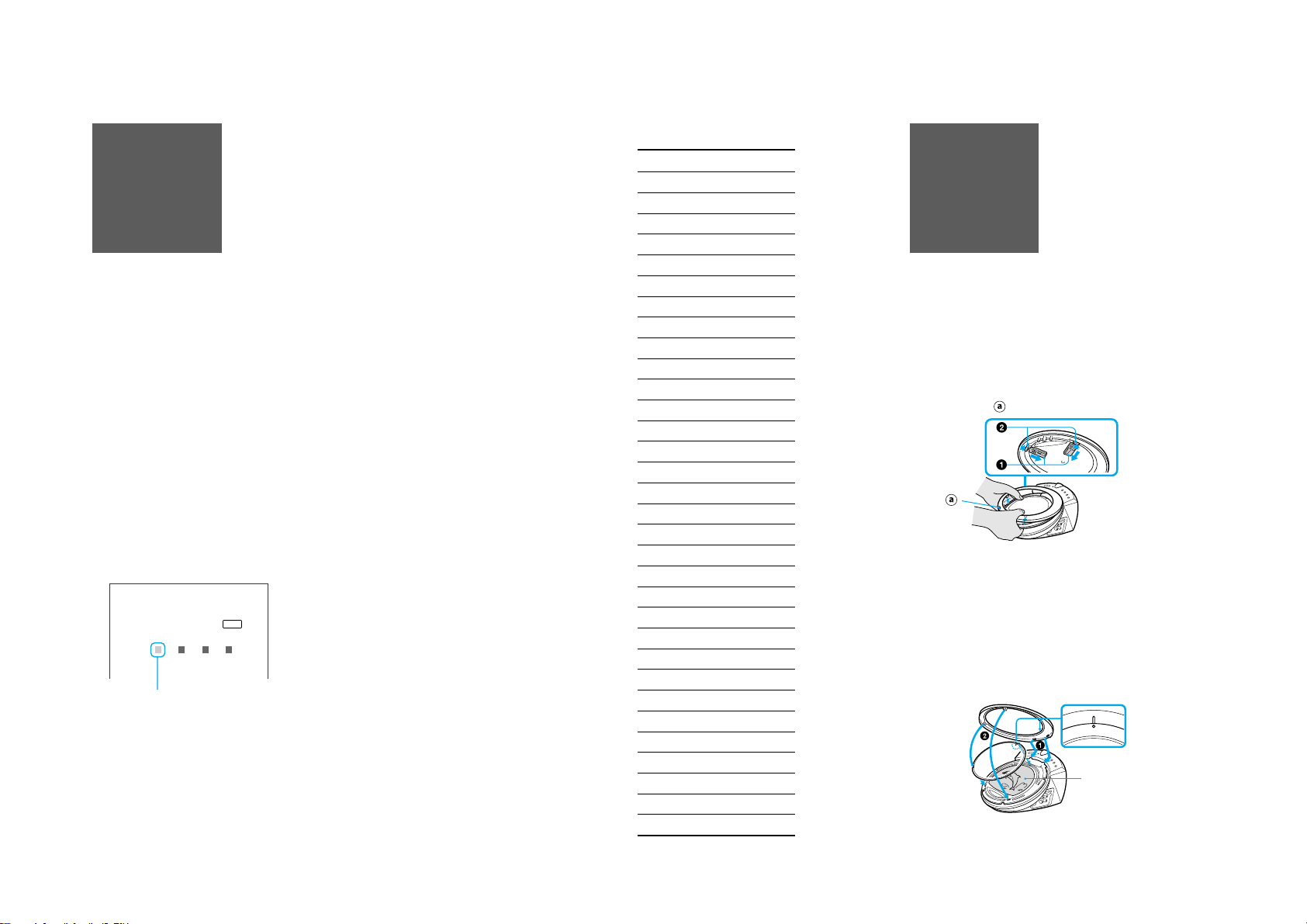
Press ZPUSH to open the lid of the player.
2
On the back side of the lid, slide the locks
toward the center (1) at the same time
as shown in the illustration and release
the hooks (2). The front part of the ring
will pop up (
3
Lower the lid and remove the ring. Then
remove the transparent cover.
4
Place a design sheet on the lid.
Replace the transparent cover, aligning
the one upper and two lower cutouts
with the lid.
5
Engage the upper two tabs of the lid with
the slots in the ring (1). Insert the two
lower tabs of the ring into the slots in the
lid (2) until it clicks.
❢
Hint
Align the marks on both the transparent cover
and the ring when replacing them.
).
design sheet
Page 8
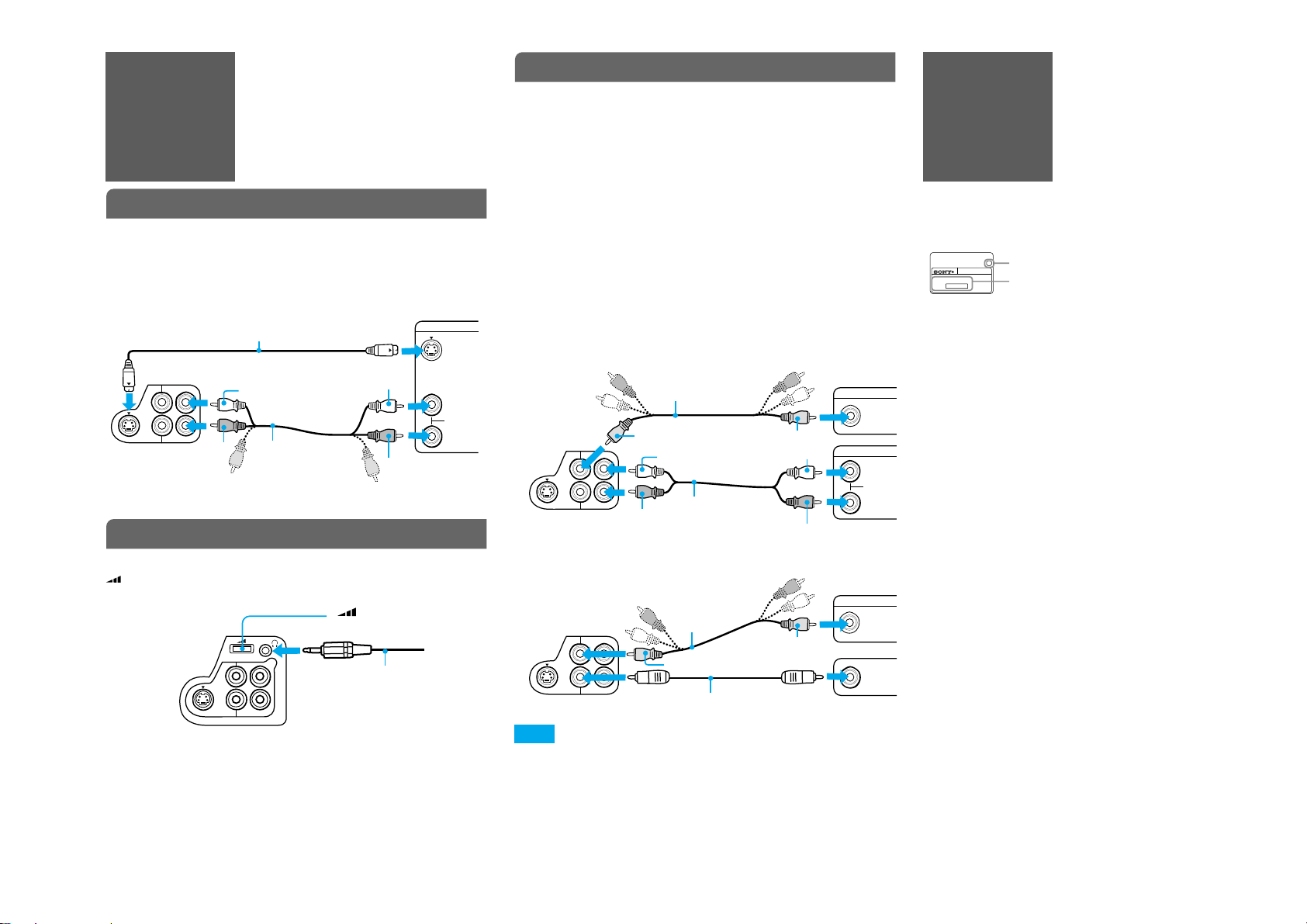
For better pictures
If your TV* has an S VIDEO input jack, connect this player to your TV
using an S VIDEO cord for higher quality images.
* You can also use monitors and projectors.
Connecting to your TV using an S VIDEO cord
For better sound
You can connect this player to an amplifier and speakers to enjoy better
sound. See the relative diagrams below to connect to an amplifier.
– A stereo amplifier: Use a stereo audio cord.
– An AV amplifier with DTS, Dolby Digital, or MPEG audio decoder: Use
a coaxial digital cord*. You can enjoy the DVD’s DTS, Dolby Digital, or
MPEG audio sound.
– An AV amplifier with Dolby Surround (Pro Logic) decoder: Use a stereo
audio cord or coaxial digital cord*. You can enjoy the DVD’s Dolby
Surround sound.
* If you connect a coaxial digital cord, you cannot use the TVS function of this
player.
Before operating this player, adjust the settings of this player (“DIGITAL
OUT”/“DOLBY DIGITAL”/“DTS”/“MPEG”) according to the connected
components (e.g., amplifier). For details, see “Settings and Adjustments”
on the Blue Side of this manual.
Connecting an amplifier using a stereo audio cord
Connecting an amplifier using a coaxial digital cord
Note
When you use the DIGITAL OUT (COAXIAL) jack to listen to MPEG audio signals
and set “MPEG” to “MPEG” in “AUDIO SETUP,” no sound will come from your
speakers if you select one of the TVS modes.
The power requirements, power consumption, and
region code of this player are indicated at the bottom
of the player. Check that the player‘s operating
voltage is identical with your local power supply.
On safety
• Caution – The use of optical instruments with this
product will increase eye hazard.
• Should any solid object or liquid fall into the
cabinet, unplug the player and have it checked by
qualified personnel before operating it any further.
On power sources (mains)
• The player is not disconnected from the AC power
source (mains) as long as it is connected to the wall
outlet, even if the player itself has been turned off.
• If you are not going to use the player for a long
time, be sure to disconnect the player from the wall
outlet. To disconnect the AC power cord (mains
lead), grasp the plug itself; never pull the cord.
On placement
• Do not install the player in an inclined position. It
is designed to be operated only in a horizontal
position.
• Place the player in a location with adequate
ventilation to prevent heat build-up in the player.
• Do not place the player on a soft surface such as a
rug that might block the ventilation holes.
• Do not place the player in a location near heat
sources, or in a place subject to direct sunlight,
excessive dust, or mechanical shock.
• Keep the player and discs away from equipment
with strong magnets, such as microwave ovens, or
large loudspeakers.
On operation
• If the player is brought directly from a cold to a
warm location, or is placed in a very damp room,
moisture may condense on the lenses inside the
player. Should this occur, the player may not
PrecautionsConnecting
Other
Components
To S-VIDEO OUT
S VIDEO cord
(not supplied)
To S VIDEO input
TV
Player
To AUDIO OUT L/R
White
Red
White
Red
Audio/video cord
(supplied)
To AUDIO OUT L/R
Audio/video cord
(supplied)
To video input
TV
Player
To audio
input
Yellow
Red
Yellow
Red
Stereo audio cord
(not supplied)
White
Amplifier
White
To VIDEO OUT
Audio/video cord
(supplied)
To video input
TV
Player
To coaxial digital
input
Yellow
Yellow
Coaxial digital cord
(not supplied)
Amplifier
To audio
input
To VIDEO OUT
To DIGITAL OUT
(COAXIAL)
Region code
Power requirements and
power consumption
AUDIO OUT
DIGITAL OUT(COAXIAL)
S-VIDEO OUT
VIDEO OUT
(R)
(L)
INPUT
VIDEO
INPUT
L(white)
R(red)
AUDIO
S-VIDEO OUT
VIDEO OUT
INPUT
VIDEO
AUDIO OUT
DIGITAL OUT(COAXIAL)
DIGITAL IN
COAXIAL
DVP-XXXX
00V 00Hz
00W
NO.
0-000-000-00
X
Connecting headphones/earphones
Connect headphones or earphones to the
i (phone) jack and adjust the
(volume) control.
Headphones/earphones
(not supplied)
To i (phone) jack
(volume) control
S-VIDEO OUT
VIDEO OUT
AUDIO OUT
L
R
DIGITAL OUT(COAXIAL)
AUDIO OUT
DIGITAL OUT(COAXIAL)
S-VIDEO OUT
VIDEO OUT
(R)
(L)
INPUT
S VIDEO
L(white)
R(red)
AUDIO
1-4
Page 9

1-5
operate properly. In this case, remove the disc and
leave the player turned on for about half an hour
until the moisture evaporates.
• Do not touch the disc if it is still spinning when
you open the lid.
• When you move the player, take out any discs. If
you don‘t, the disc may be damaged.
On the headphones/earphones
Preventing hearing damage
Avoid using headphones/earphones at high volumes.
Hearing experts advise against continuous, loud and
extended play. If you experience a ringing in your
ears, reduce the volume or discontinue use.
Caring for others
Keep the volume at a moderate level. This will allow
you to hear outside sounds and to be considerate of
the people around you.
On cleaning
Clean the cabinet, panel, and controls with a soft cloth
slightly moistened with a mild detergent solution. Do
not use any type of abrasive pad, scouring powder, or
solvent such as alcohol or benzine.
On cleaning discs
Do not use a commercially available cleaning disc. It
may cause a malfunction.
IMPORTANT NOTICE
Caution: This player is capable of holding a still video
image or on-screen display image on your television
screen indefinitely. If you leave the still video image or
on-screen display image displayed on your TV for an
extended period of time, you risk permanent damage
to your television screen.
Plasma Display Panel televisions and projection
televisions are especially susceptible to this.
If you have any questions or problems concerning
your player, please consult your nearest Sony dealer.
Notes about discs
• To keep a disc clean, handle it by its edge. Do not
touch the surface.
• Do not expose the disc to direct sunlight or heat
sources such as hot air ducts, or leave it in a car
parked in direct sunlight as the temperature may
rise considerably inside the car.
• After playing, store the disc in its case.
• Clean the disc with a cleaning cloth. Wipe the disc
from the center out.
• Do not use solvents such as benzine, thinner,
commercially available cleaners, or anti-static
spray intended for vinyl LPs.
Troubleshooting
If you experience any of the following
difficulties while using the player, use this
troubleshooting guide to help remedy the
problem. Should any problem persist, consult
your nearest Sony dealer.
Power
The player does not turn on.
1
Connect the power cord (mains lead)
securely.
1
Close the lid of the player until it clicks.
Display
There is no picture.
The picture is distorted.
1
Check to see if the player is connected
securely.
1
Check to see if the connecting cord is
damaged.
1
Check the connection and change the video
input on the TV so that the picture output
from this player is displayed on the TV
screen.
1
If the video signal from your DVD player is
output to your TV via a VCR, the copyprotection signal of some DVD programs
could affect the picture quality. If you still
experience problems after connecting this
player directly to your TV, try connecting to
the S VIDEO input of your TV, if it has one.
The picture does not fill the screen even
after adjusting the “TV TYPE” in “DISPLAY
SETUP.”
1
The aspect ratio is fixed on your DVD.
Audio
There is no sound.
1
Check to see if the player is connected
securely.
1
Check to see if the audio connecting cord is
damaged.
1
Check to see if the player is connected
correctly to the amplifier.
1
Change the audio input setting of your
amplifier so that you can hear the sound
from this player.
1
The player is in the pause, Slow Motion
Play, or the scan mode.
1
If no sound is output from the DIGITAL
OUT (COAXIAL) jack, check the audio
setup setting. (See “Settings and
Adjustments” on the Blue Side.)
1
Press AUDIO repeatedly and select
“STEREO” to play DTS sound tracks on a
CD.
A loud noise occurs.
1
When playing a CD with DTS sound tracks,
noise will come from the AUDIO OUT L/R
jacks.
The volume is low.
1
Select “ON” for “AUDIO ATT” in the audio
setup setting. (See “Settings and
Adjustments” on the Blue Side.)
1
If you are playing a Super VCD which does
not contain a second audio track, no sound
will come out when you select “2:
STEREO,” “2: 1/L,” or “2: 2/R” by pressing
AUDIO repeatedly.
There is no sound output from the
headphones/earphones or the sound is
too low.
1
Insert the headphones/earphones plug
firmly into the i jack.
1
Adjust the (volume) control.
Operation
The remote does not function.
1
Remove any obstacles between the remote
and the player.
1
Use the remote near the player.
1
Point the remote at the remote sensor on
the player.
1
Replace all batteries in the remote with new
ones.
The disc does not play.
1
Close the lid of the player until it clicks.
1
Place the disc on the tray with the recorded
side facing down, and press its center until
it clicks into place.
1
The disc type is not compatible with the
player.
1
Moisture has condensed inside the player.
(See “Precautions” for details.)
The player does not start playing from
the beginning of a disc.
1
The player is in Repeat Play, Shuffle Play, or
Resume Play mode. To return to normal
play mode, press CLEAR or press x twice.
Playback stops automatically.
1
A disc with an auto pause signal stops
playback at that signal.
I cannot perform some functions such as
Stop, Scan, Slow Motion Play, Repeat Play,
or Shuffle Play.
1
Some discs prohibit the operation of these
functions.
Page 10

1-6
I cannot switch the audio language or the
angle.
I cannot change the subtitle language or
cancel the subtitles.
1
Instead of pressing AUDIO, ANGLE, or
SUBTITLE, press MENU to display the
DVD’s menu and select the desired option
with B/V/v/b and ENTER.
1
There are no multilingual tracks, subtitles,
or multi-angles recorded on that DVD.
1
There are no other recorded angles for the
scene you are watching.
1
The changing of language, angle, or
subtitles is prohibited on that DVD.
The player does not operate properly.
1
Static electricity, etc., may affect the player's
operation.
Disconnect the AC power cord (mains
lead), then connect it again.
Error Messages
A five-character service number
(combination of a letter and digits (e.g.,
“E:61:10”)) is displayed on the screen.
1
When the first 3 digits are “C13”:
Clean the disc with a cleaning cloth.
1
When the first 3 digits are “C31”:
Place the disc correctly on the tray.
1
When the digits start with “E”:
Consult your nearest Sony dealer.
Specifications
System
Laser: Semiconductor laser
Signal format system:
Outputs
(Jack name: Jack type/Output level/
AUDIO OUT L/R: Phonojack/2 Vrms/10 kΩ
DIGITAL OUT (COAXIAL): Phonojack/0.5 Vp–p/75 Ω
VIDEO OUT: Phonojack/1.0 Vp–p/75 Ω
S-VIDEO OUT: 4 -pin mini DIN/
Headphones/earphones:
General
Power requirements:
Power consumption: 9 W
Dimensions (approx.): 190 × 147 × 235 mm
Mass (approx.): 1.3 kg (2.9 lbs)
Operating temperature: 5 °C to 35 °C (41 F to 95 F)
Operating humidity: 25 - 80 %
Supplied accessories
Operating Instructions (1)
Audio/video cord (1)
Remote (1)
AA (R6) size batteries (2)
EURO AV adaptor (For European models only) (1)
Design sheet
Specifications and design are subject to change
without notice.
NERGY STAR
E
NERGY STAR
E
determined that this product meets the E
guidelines for energy efficiency.
U.S./Canadian models: NTSC
European models: PAL/NTSC
Load impedance)
Y: 1.0 Vp–p,
C: 0.3 Vp–p (PAL), 0.286 Vp–p (NTSC)/
75 Ω
Stereo mini-jack/9 mW + 9 mW/32 Ω
U.S./Canadian models: 120 V AC, 60 Hz
European models: 220 - 240 V AC,
50/60 Hz
7
/8 × 9 in.) (w/h/d)
(7 × 5
®
is a U.S. registered mark. As an
®
Partner, Sony Corporation has
NERGY STAR
Language Code List
The language spelling conforms to the ISO 639:1988 (E/F) standard.
Code Language Code Language Code Language Code Language
1349 Macedonian
1350 Malayalam
1352 Mongolian
1353 Moldavian
1356 Marathi
1357 Malay
1358 Maltese
1363 Burmese
1365 Nauru
1369 Nepali
1376 Dutch
1379 Norwegian
1393 Occitan
1403 (Afan)Oromo
1408 Oriya
1417 Punjabi
1428 Polish
1435 Pashto;
Pushto
1436 Portuguese
1463 Quechua
1481 Rhaeto-
Romance
1482 Kirundi
1483 Romanian
1489 Russian
1491 Kinyarwanda
1495 Sanskrit
1498 Sindhi
1501 Sangho
1502 Serbo-
Croatian
1503 Singhalese
1505 Slovak
1506 Slovenian
1507 Samoan
1508 Shona
®
1027 Afar
1028 Abkhazian
1032 Afrikaans
1039 Amharic
1044 Arabic
1045 Assamese
1051 Aymara
1052 Azerbaijani
1053 Bashkir
1057 Byelorussian
1059 Bulgarian
1060 Bihari
1061 Bislama
1066 Bengali;
Bangla
1067 Tibetan
1070 Breton
1079 Catalan
1093 Corsican
1097 Czech
1103 Welsh
1105 Danish
1109 German
1130 Bhutani
1142 Greek
1144 English
1145 Esperanto
1149 Spanish
1150 Estonian
1151 Basque
1157 Persian
1165 Finnish
1166 Fiji
1171 Faroese
1174 French
1181 Frisian
1183 Irish
1186 Scots Gaelic
1194 Galician
1196 Guarani
1203 Gujarati
1209 Hausa
1217 Hindi
1226 Croatian
1229 Hungarian
1233 Armenian
1235 Interlingua
1239 Interlingue
1245 Inupiak
1248 Indonesian
1253 Icelandic
1254 Italian
1257 Hebrew
1261 Japanese
1269 Yiddish
1283 Javanese
1287 Georgian
1297 Kazakh
1298 Greenlandic
1299 Cambodian
1300 Kannada
1301 Korean
1305 Kashmiri
1307 Kurdish
1311 Kirghiz
1313 Latin
1326 Lingala
1327 Laothian
1332 Lithuanian
1334 Latvian;
Lettish
1345 Malagasy
1347 Maori
1509 Somali
1511 Albanian
1512 Serbian
1513 Siswati
1514 Sesotho
1515 Sundanese
1516 Swedish
1517 Swahili
1521 Tamil
1525 Telugu
1527 Tajik
1528 Thai
1529 Tigrinya
1531 Turkmen
1532 Tagalog
1534 Setswana
1535 Tonga
1538 Turkish
1539 Tsonga
1540 Tatar
1543 Twi
1557 Ukrainian
1564 Urdu
1572 Uzbek
1581 Vietnamese
1587 Volapük
1613 Wolof
1632 Xhosa
1665 Yoruba
1684 Chinese
1697 Zulu
1703 Not specified
Page 11
Connecting to your TV
You can enjoy standard quality picture and sound using this
connection. Before connecting, make sure that your TV is turned off.
To enjoy better picture and sound, refer to the Brown Side of this
manual. Refer also to the instruction manuals of the components to
be connected.
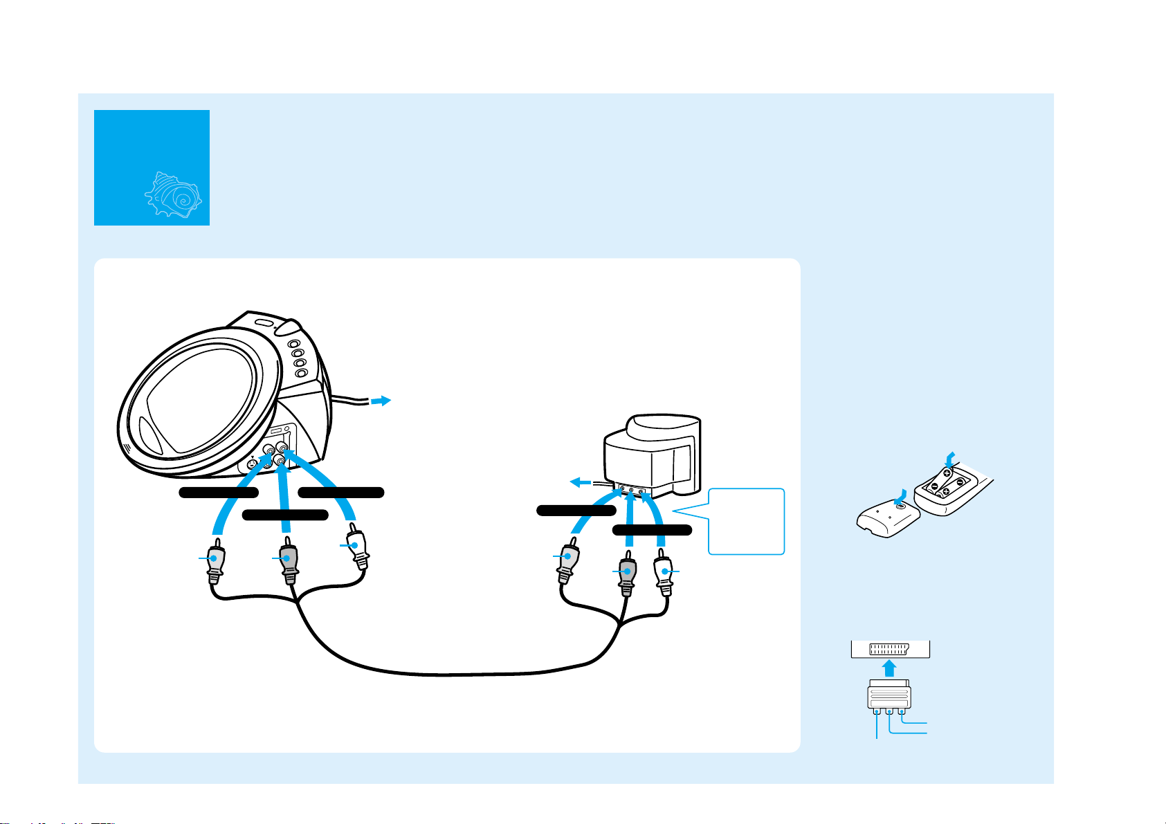
Connecting
the Player
Basic connection
White
RedYellow
White
Red
Yellow
Notes on connecting to your TV
• Do not connect this player directly to a
component such as a VCR. If you do, noise
may appear in the picture.
• When connecting this player to a monaural
TV, use a stereo-mono conversion cord (not
supplied).
To insert batteries in the remote
Slide open the cover. Insert two AA (R6) size
batteries by matching the + and – ends with
the markings inside the compartment, and
close the cover.
Connecting the EURO AV Adaptor
(For European models only)
Attach the Euro AV Adaptor (supplied) to your
TV. Then, connect the audio/video cord to the
corresponding jacks of the Euro AV Adaptor.
TV
Connect the audio/video cord (supplied).
Then, connect the player and the TV to an AC power source (mains).
AC power
source (mains)
AC power
source (mains)
TV
Video input
Audio input (R)
Audio input (L)
To AUDIO OUT R
To VIDEO OUT
To AUDIO OUT L
To audio input
To video input
For European
models only:
Connect using the
EURO AV Adaptor
(supplied).
1-7
Page 12
1-8
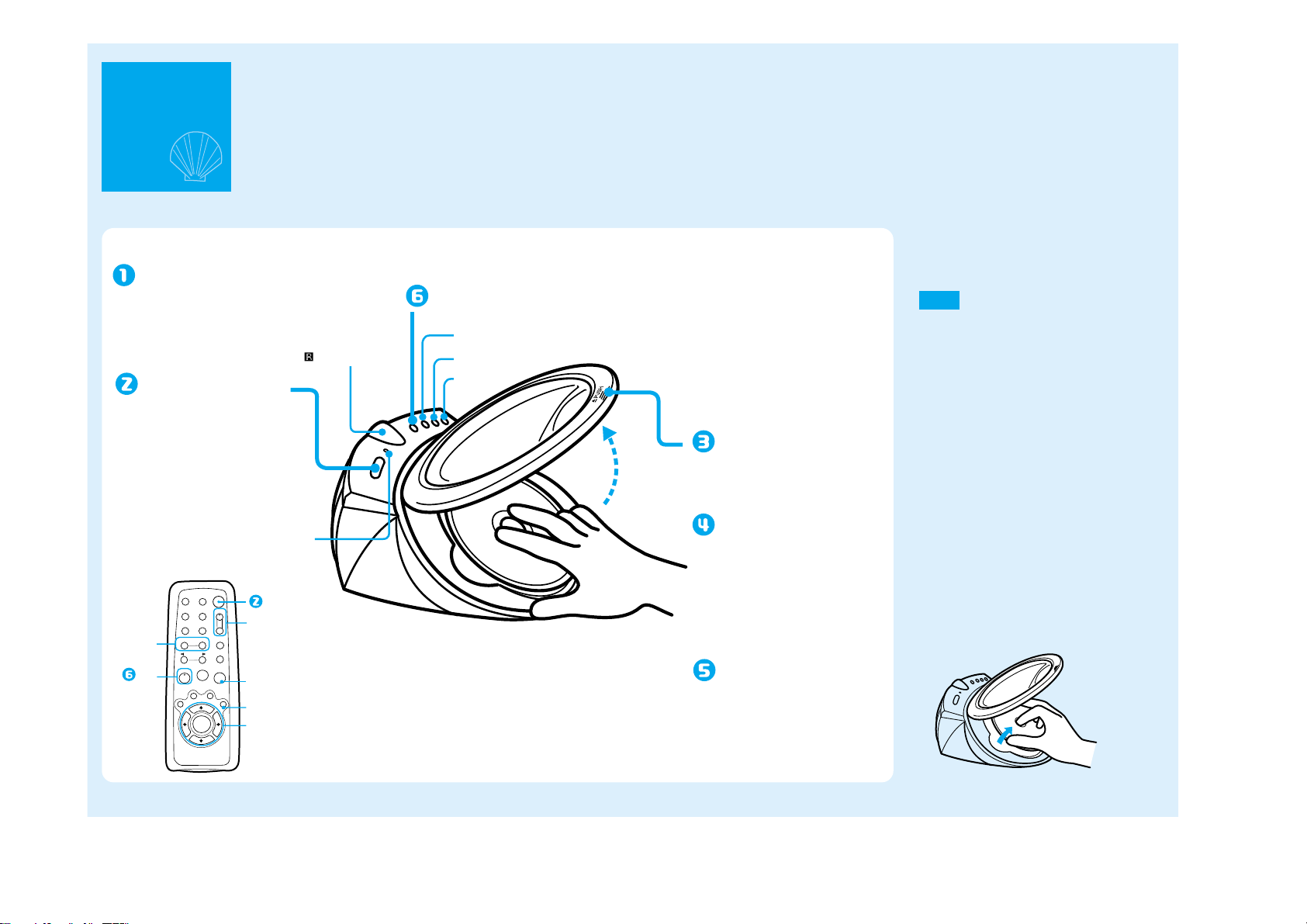
Playing
Discs
On your TV :
Turn your TV on and
select the video input.
Turn on the player
by pressing ?/1
(on/standby).
One of the background
pictures appears at random
on your TV screen.
=/1
REPEAT SUR
SHUFFLE AUDIO
TV VOL
+
ANGLESUBTITLE
−
PREV NEXT
DISPLAY
.
SCAN/SLOW
m
PLAY
H
TOP MENU
CLEAR
>
REPLAY
M
PAUSE
STOP
X
x
MENU
RETURN
O
ENTER
./ >
H
Basic steps and tips on playback
You can play DVDs, VIDEO CDs, music CDs, as well as MP3 audio
tracks recorded on a DATA CD*.
Buttons on the player that share the same symbol with buttons on
the remote also share the same function.
*A CD-R/CD-RW/CD-ROM with MP3 audio tracks recorded on the disc is called a “DATA CD” in
this manual.
Press H (play).
x (stop)
(remote sensor)
?/1 indicator
Lights up when
turned on.
?/1
TV VOL (volume) +/–
x
O
B/V/v/b/ENTER
. (previous)
> (next)
Press ZPUSH, and
gently lift the lid
until it clicks.
Place a disc on the
tray.
Place it label-side up (the
recorded side facing down),
and press its center until it
clicks into place.
Close the lid until it
clicks.
To adjust the TV volume (for Sony
products only)
Press TV VOL +/–.
Note
This function may not be available depending on the
connected TV.
To play the next or previous
chapter or track
Press > or . during playback.
To stop playback
Press x.
The background picture appears on your TV
screen. (See “Settings and Adjustments” for
details.)
The next time you press H, playback starts
from the same place. (Resume Play)
To play from the beginning
Press x twice, then press H.
To remove the disc
Hold the edges of the disc and pull while
pressing the center.
See “Using the remote” at the bottom half of this
page for more details on the remote.
Page 13

1-9
1
(
3 0
)
ROCK BEST HIT
KARAOKE
JAZZ
R&B
MY FAVORITE SONGS
CLASSICAL
SALSA OF CUBA
BOSSANOVA
JAZZ
1 ( 9 0
)
01SHE IS SPECIAL
02ALL YOU NEED IS ...
03SPICY LIFE
04HAPPY HOUR
05RIVER SIDE
06
5
07TAKE TIME,TAKE TIME
To turn off the player
Press ?/1.
If no buttons are pressed for 10 minutes, the
screensaver turns on. To return to the normal
screen, press H. (To turn off the screensaver,
see ”Setting and Adjustments” for details.)
The player automatically turns off in another
50 minutes.
If a menu display appears when
you press H
In some DVDs and VIDEO CDs, a menu may
appear when you press H. The menu usually
enables you to select items such as a title
(movie or album), audio language, or subtitles
by using B/V/v/b and ENTER. In VIDEO
CDs, this function is called PBC (Playback
Control).
To return to the menu display while playing
a disc with PBC function
Press O.
To play a disc without using the PBC
function
Press > or . during stop to select a track
(picture or music) that you want to play, and
press H or ENTER.
To return to PBC Playback
Press x twice, and press H.
Operating the remote
• Point the remote at the remote sensor .
When it does not work, operate closer to the
remote sensor
• Do not expose the remote sensor
.
to direct
sunlight or lighting apparatuses. Doing so
may cause a malfunction.
If the aspect ratio of the picture
does not match your TV type
In “TV TYPE” of the screen setup setting,
select the setting that matches your TV. (See
“Settings and Adjustments” for details.)
Playing MP3
audio tracks
from a list
You can select and play MP3 audio tracks from
the list displayed on the menu.
Selecting an MP3 audio track
1
Press MENU.
Albums containing MP3 audio tracks appear.
<TV screen>
Selected album number
Number of playable albums in
the disc
album
list
2
Select an album using V/v, and press
ENTER.
The MP3 audio tracks contained in the album
appears.
<TV screen>
Selected track number
Number of playable tracks in the
album
track list
To display the next or previous page in an
album or track list
Press b or B.
To return to the previous screen
Press O.
To turn off the menu
Press MENU once.
❢
Hint
The album or track currently being played is shaded
in the list.
Notes
On playback
• Only the MP3 audio tracks displayed in the list can
be played on this player (maximum 100 albums or
200 tracks).
• MP3 audio tracks are played in the order displayed
in the list. This may not coincide with the recorded
order.
• The following audio format files cannot be played.
– MP3 audio tracks not created according to
ISO9660 Level1/Level2/Joliet.
– MP3 audio tracks that do not have the file name
extension “.MP3.”
– Files with the file name extension “.MP3,” but
are not MP3 audio tracks.
– Audio tracks recorded in MP3PRO format.
– MP3 audio tracks recorded in Packet Write
format.
– Data that are not MPEG1 Audio Layer 3.
On the display method
• Only the alphabet and numbers can be displayed.
Other characters appear as an “*” (asterisk).
• This player cannot display ID3 tags.
3
Select a track using V/v, and press
ENTER.
Playback starts.
Page 14
Using the
Remote
✎
To change the playing mode, sound
effect, and display, or to use the DVD’s
menu.
c
“Functions”
✎
To read disc information on the screen.
c
“Reading the screen”
Remote
The letters below correspond to the letters in
“Functions.” Use the letters to quickly find the
buttons needed for each operation.
Press to
turn the
player on.
Press to
adjust the
volume of
Sony TVs.
Press to
cancel the
current
mode.
Functions
Note
Some playback features of DVDs and VIDEO CDs described in the following may be prohibited
by the software producers. Refer to the instructions supplied with the DVDs and VIDEO CDs.
Basic operations (A)
To Press
play H
stop x
pause X
> NEXT or .PREV during playback.
My or my during playback.
Press the button repeatedly to change the speed.
To return to normal playback, press H.
My or my during pause. (DVD/VIDEO CD only.
Functions only in the forward direction for VIDEO CDs.)
Press the button repeatedly to change the playback speed.
To return to normal playback, press H.
replay REPLAY during playback. (DVD only)
Selecting the playing mode (B)
You can play a selected title or track randomly or repeatedly.
To cancel the operation, press the following button repeatedly to select “OFF” or
press CLEAR.
To Press
shuffle SHUFFLE repeatedly during playback. (DVD/VIDEO CD/CD
only)
repeat REPEAT repeatedly during playback.
When you select Repeat Play during Shuffle Play, Shuffle Play is
repeated.
Changing the sound (C)
You can change the audio language for DVDs recorded with multilingual tracks.
When listening to a Karaoke VIDEO CD, you can turn off the vocals. You can also
enjoy this player’s surround effect mode.
To change Press
language/sound AUDIO repeatedly during playback to select from the options.
In DVDs: Select a language from the options on the screen.
(When a 4-digit number is displayed, check the number in the
“Language Code List” on the Brown Side of this manual.)
VIDEO CDs/CDs/DATA CDs:
• STEREO: To hear standard stereo sound.
• 1/L: To hear the sound of the left channel from both speakers.
• 2/R: To hear the sound of the right channel from both speakers.
Super VCDs:
(The number before the colon shows the number of the audio
track being played. For the meaning after the colon, see above.)
• 1: STEREO • 2: STEREO
• 1: 1/L • 2: 1/L
• 1: 2/R • 2: 2/R
SUR repeatedly during playback to select from the following.
(DVD only)
To cancel the surround setting, press SUR repeatedly to select
“OFF.”
•TVS DYNAMIC: To enjoy the surround effect with your TV’s
speakers. The distinct sound imaging effect is as if you have a
set of additional speakers next to you.
• TVS WIDE: To enjoy the surround effect with your TV’s
speakers. The sound imaging effect is as if you have five sets
of virtual speakers filling the area surrounding you.
• TVS NIGHT: To enjoy the surround mode at a lower volume.
(Dolby Digital audio DVD only)
• TVS STANDARD: To enjoy the surround effect with a set of
front speakers connected to the player. The imaging effect is as
if you have three sets of additional speakers around you.
scan forward or
backward
play forward or
backward in
slow motion
TV Virtual
Surround settings
Notes
• The surround mode
signals are only
output when the
player is connected
via the AUDIO OUT
L/R jack.
• Set the surround
settings of the
connected
components (such as
TV) to off.
• Surround does not
function when a disc
has no rear signal.
B
C
D
E F
A
go to the next or
previous title or
track
O
TOP MENU
=/1
TV VOL
CLEAR
REPLAY
STOP
PAUSE
PLAY
PREV NEXT
ANGLESUBTITLE
SHUFFLE AUDIO
REPEAT SUR
RETURN
MENU
DISPLAY
ENTER
x
X
H
.
>
m
M
+
−
SCAN/SLOW
There is a tactile dot on H and the “+” button of
TV VOL.
1-10
Page 15
1-11
T11 — 8 T 1:01:57
DOLBY DIGITAL
3 /2 .1
Changing the viewing angle and subtitles (D)
You can select picture angles if there are multiple pictures (angles) recorded on the
disc, or change subtitle languages in multilingual DVDs.
To Press
change angles ANGLE repeatedly during playback to select the number of the
display or
change subtitles
angle you want to play. (DVD only)
SUBTITLE repeatedly to select the subtitle language. (DVD only)
(When a 4-digit number is displayed, check the number in the
“Language Code List” on the Brown Side of this manual.)
To cancel the subtitle, press SUBTITLE repeatedly to select
“OFF.”
Using the DVD’s menu (E)
When a menu is recorded on the DVD, you can usually select items such as the
title, audio language, or subtitles.
To display Press
DVD’s menu TOP MENU or MENU. Select an item using B/V/v/b, and
press ENTER. (DVD only)
TOP MENU: Displays a menu of available movie and music
titles.
MENU: Displays a menu of subtitles and audio languages.
Displaying information on your screen (F)
You can display information such as the playing time or the disc text on the TV
screen.
To return to the normal screen, press DISPLAY repeatedly.
To display Press
time/text DISPLAY during playback. Then press ENTER repeatedly to
current audio
format
switch the display from total playing time to remaining time,
and vice versa. (For details, see “Time display” in the next
section.)
DVD/CD TEXT or MP3 track name will be displayed following
the time display if it is recorded on the disc. (Only the letters of
the alphabet are shown.)
DISPLAY twice during playback. (DVD only)
(For details, see “Audio display” in the next section.)
Reading the screen
You can display the time or audio format in the
upper area of the TV screen during playback.
Time display
<Example*>
*Here, the disc is playing chapter 8 of the 11th title, which has
been played for 1 hour 1 minute and 57 seconds.
Audio display
<Example*>
*Here, the indicated disc’s audio format is Dolby Digital
5.1channel (ch).
5.1ch: 3 (Front Left/Right/Center) +
Note
When “DTS” is set to “OFF” in the audio setup
setting, the DTS display will not appear even if the
disc has a DTS signal. (See “Settings and
Adjustments” for details.)
Current album/title
number
• T: title, A: album
Current chapter/
track/index number
Current audio format (Dolby
Digital, DTS, PCM,etc.)
Number of front and
center component
2 (Rear Left/Right) +
0.1 (LFE)
Time display
• D: disc, T: title or track,
C: chapter
• No mark: Playing time
With – : Remaining time
Number of rear
component
Number of LFE
(Low Frequency Effect)
component
Settings
and
Adjustments
You can select and change the settings of this
player to meet your needs and to suit your
playing environment.
To change the languages used in
✎
subtitles, sound, or on-screen displays.
“Language/Screen/Audio Setup”
c
To adjust the aspect ratio of the picture
✎
to fit your TV.
“Language/Screen/Audio Setup”
c
To select the setting of the audio when
✎
connected to an amplifier.
“Language/Screen/Audio Setup”
c
To set playback limitation levels (such as
✎
to limit violent scenes).
“Limiting Playback” (See the
c
Brown Side of this manual.)
Page 16

1-12E
Language/Screen/Audio Setup
You can change the languages for the OSD (onscreen display) and sound, and adjust the
video and audio output to match the
components (such as TV) your player is
connected to.
Setup Display
The numbers correspond to the steps in the procedure given
below.
23
LANGUAGE SETUP
OSD:
MENU:
AUDIO:
SUBTITLE:
1
Press DISPLAY repeatedly in stop mode to
show Setup Display.
2
Select the setup item using V/v, and press
ENTER.
LANGUAGE SETUP: To change the
language setting.
SCREEN SETUP: To change the screen
setting.
AUDIO SETUP: To change the audio
setting.
3
Select an item (e.g., “OSD”) using V/v,
and press ENTER.
Refer to the list on the right for details.
4
Select a setting (e.g., “ENGLISH”) using
V/v, and press ENTER.
Refer to the list on the right for details.
To turn off Setup Display:
Press DISPLAY repeatedly until the display
disappears.
ENGLISH
ENGLISH
ORIGINAL
AUDIO FOLLOW
4
Selecting the language setup
For the following items, select the language from the Language List
displayed on the screen.
Item Select
OSD The language you want for the player’s menu and the
MENU*
(DVD only)
AUDIO*
(DVD only)
SUBTITLE*
(DVD only)
* If the language you select here is not recorded on the disc, another language will
be automatically selected from the disc.
❢
Hint
When you select “OTHERS,” enter the language code from the list on the Brown
Side of this manual using V/v/b.
Setup Display.
The language you want for the menu recorded on the
disc.
The language you want for the sound.
(ORIGINAL: The language prioritized in the disc is
automatically chosen.)
The subtitle language.
(AUDIO FOLLOW: The subtitle language changes
according to the audio language.)
Selecting the screen setup
Item Select
TV TYPE*
(Change this to fit
the picture to your
TV.)
SCREEN SAVER
• 16:9
•
4:3 LETTER BOX
• 4:3 PAN SCAN
For a wide-screen TV or a TV
with wide mode function.
For a standard TV. Displays a
wide picture to fit the width of
the screen while keeping the same
aspect ratio.
For a standard TV. Cuts off
portions of a wide picture in
order to fit the width of the
screen.
•ON: Turns on the screen saver.
•OFF: Turns off the screen saver.
BACKGROUND
•1: The logo appears.
•2: A preset picture appears.
•3: A preset picture appears.
PAR E NTAL
CONTROL
* The setting recorded on the disc has priority.
(See “Limiting Playback” on the Brown Side for
instructions.)
Selecting the audio setup
Item Select
AUDIO ATT
(Audio attenuation)
DIGITAL OUT
(Adjust only when
using a coaxial
digital cord.)
DOLBY DIGITAL
(Adjust only when
“DIGITAL OUT” is set
to “ON.”)
MPEG
(For European models
only)
(Adjust only when
“DIGITAL OUT” is set
to “ON.”)
DTS
(Adjust only when
“DIGITAL OUT” is set
to “ON.”)
❢
Hint
The underlined settings are the default settings.
• OFF: Standard setting.
• ON: When the playback sound is distorted.
(See “Connecting Other Components” on the Brown
Side of this manual for instructions on this
connection.)
• OFF: When connecting a TV or an amplifier to
AUDIO OUT L/R.
ON: When connecting an amplifier with a digital
•
input jack, etc., to DIGITAL OUT (COAXIAL).
(See “Connecting Other Components” on the Brown
Side for instructions on this connection.)
D-PCM: Standard setting.
•
• DOLBY DIGITAL: When connecting to an amplifier
with a built-in Dolby Digital decoder.
(See “Connecting Other Components” on the Brown
Side for instructions on this connection.)
•
PCM: Standard setting.
• MPEG: When connecting to an amplifier with a
built-in MPEG audio decoder.
(See “Connecting Other Components” on the Brown
Side for instructions on this connection.)
•
OFF: Standard setting.
• ON: When connecting to an amplifier with a
built-in DTS decoder.
Page 17
SECTION 2
DISASSEMBLY
Note: Follow the disassembly procedure in the numerical order given.
DVP-PQ2
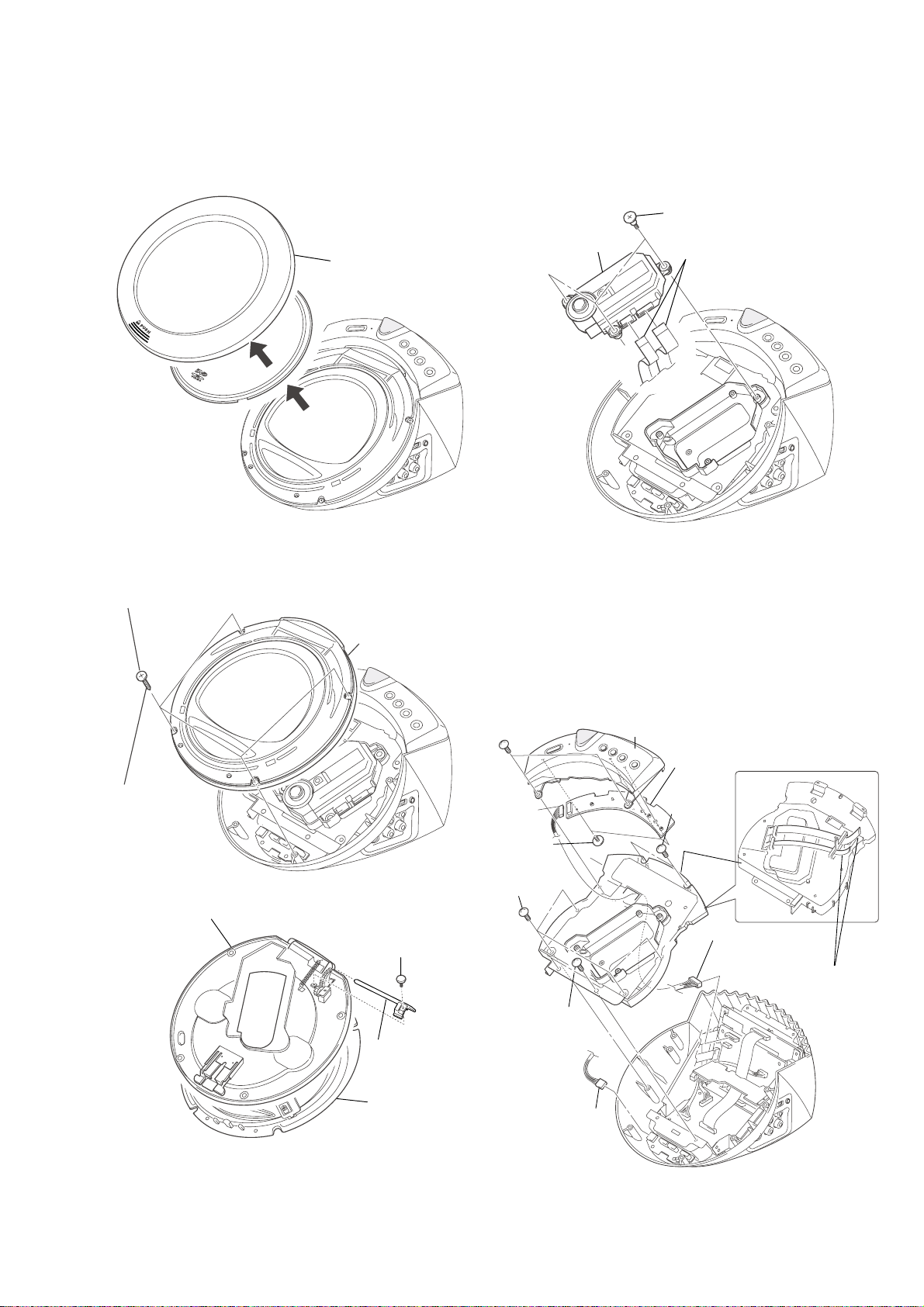
2-1. LID ASSEMBLY REMOVAL
Ring
1
2-2. DISK BASE ASSEMBLY REMOVAL
1 Four ornamental sheets (screw)
2-3. BASE UNIT REMOV AL
1 Three INS screws
2 Base unit
3 Two flexible flat cables
(FMP-006, 005)
2 Four ornamental
screws (M3 x 12)
Disk Base
4
3 Disk base assembly
One Screw
1
(M2x8)
Shaft (LID)
2
2-4. BU HOLDER REMOV AL
3Two screws
(+BV3 x 10)
6 Three screws
(M2 x 8)
7 Four screws
(+BV3 x 10)
7 Two screws
(+BV3 x 10)
4 SW panel assembly
0 SW 406 board
5 Two screws
8 BU holder
(+BV3 x 10)
1 Flexible flat cable
Harness
(IS-059)
(CN811)
9 Flexible flat cable
(CN203)(CN204)
Lid assy
3
Note: When you tighten four screws, in order not to make a crevice
between a disk base and a lower case, please hold from both
sides.
2-1
2Connector
(CN950)
Page 18

2-5. SW-406 BOARD REMOV AL
1 SW 406 board
2-7. LOWER CASE REMOVAL
2 Power cord connector
2 Three screws
(M2 x 8)
2-6. HP-137 BOARD &
JACK PLA TE REMOVAL
5 One screw
(+BV 3 x 6)
4 HP-137 board
1 Lower case
2-8. POWER SWITCHING REGULAT OR
BLOCK REMOVAL
3 Power switching
regulator block
2 Four screws
(+BV3x
6)
3
Jack plate
2
1 Three screws (+BV3x10)
(black)
1 Connector
2-2
Page 19
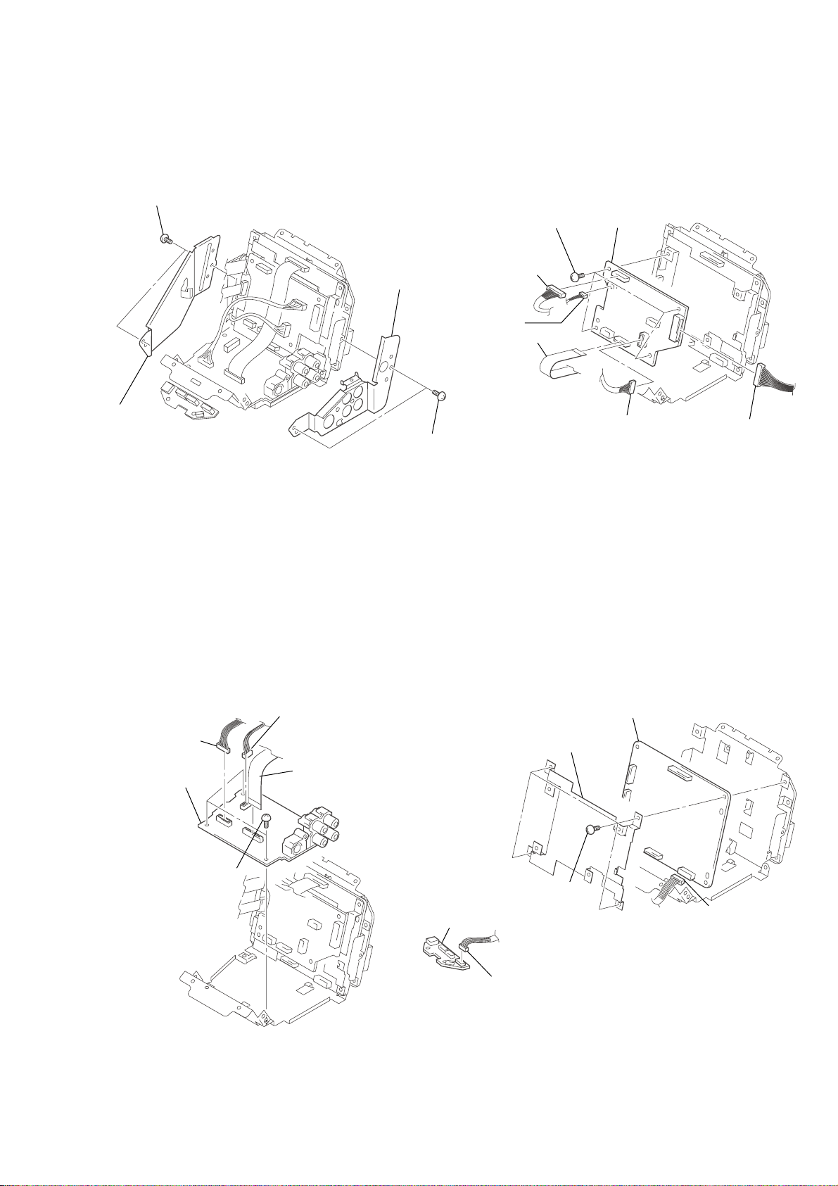
2-9. SHIELD PLA TE REMOVAL
5 Four screws
(+BV3x6)
4 IF-106 board
1 Flexible flat cable
(FIM-001)
(CN807)
2 Two connector
(CN809)
3 Connector
(CN801)
7 Connector
(CN812)
6 Connector
(CN811)
3 Two screws (+BV3x6)
4 Shield plate
2-11. IF-106 BOARD REMOV AL
2 Shield plate (jack)
1 Two screws (+BV3x6)
2-10. A V -77 BOARD REMOV AL
2 Connector
(CN301)
4 AV-77 board
3 Three screws (B3)
(+BV 3 x 6)
5 Connector
(CN500)
1 Flexible flat cable
(FMV-021)
(CN100)
2-12. MB-108 & SW-407 BOARDS REMOV AL
3 MB-108 board
2 Chassis (MB)
1 Four screws
(+BV3 x 6)
4 SW-407 board
5 Connector
(CN951)
6 Connector
(CN103)
2-3
Page 20
2-13. CIRCUIT BOARDS LOCA TION
SW-406
(FUNCTION SWITCH)
IF-106
(INTERFACE CONTROL)
HP-137
(HEADPHONE)
SWITCHING REGULATOR
DPSN-20CP (PQ2: U2,CA2,MX2)
DPSN-20CP-2 (PQ2: EC1,EC2,CEK)
SW-407
(DOOR SWITCH)
MB-108
(SIGNAL PROCESS, SERVO)
AV-77
(AUDIO/VIDEO OUT)
2-4 E
2-4
Page 21
3-1. OVERALL BLOCK DIAGRAM
DVP-PQ2
SECTION 3
BLOCK DIAGRAMS
BASE UNIT
KHM-295AHA/
SERVICE ASSY
OPTICAL DEVICE
DVD/CD
PD IC
FOCUS
COIL
TRACKING
COIL
INLIMIT
SENSOR
SPINDLE
MOTOR
SLED
MOTOR
MB-108 BOARD
(SEE PAGE 4-9 to 4-20)
IC303
16M DRAM
RF
MM
MM
IC201
DVD/CD RF AMP,
DIGITAL SERVO
IC202
FOCUS/TRACKING
COIL DRIVE,
SPINDLE/SLED/
LOADING
MOTOR DRIVE
RF+
SERVO DSP
IC106
16M FLASH
IC301
ARP,
or
IC101
EEPROM
IC107
OTP
SDI 0 – 7
CDDOUT, CDDATA,
CDBCK, CDLRCK
PARALLEL BUS
SYSTEM
CONTROL
IC404
IC104
(PQ2: EC1,EC2,CEK)
IC405
16M SDRAM
IC403
AV DECODER
SPDIF, ACH12,
ACH34, ACH56,
BCK, LRCK
SPDIF
IC601
AUDIO
D/A CONVERTER
AV-77 BOARD
(SEE PAGE 4-23)
V, Y, C
IC101
VIDEO
BUFFER
IC202
AUDIO
AMP
J100
S-VIDEO OUT
J201 (1/3)
VIDEO OUT
J201 (2/3)
DIGITAL OUT
(COAXIAL)
J201 (3/3)
L
AUDIO OUT
R
HP-137 BOARD
(SEE PAGE 4-37)
IC501
AUDIO
AMP
J501
AC IN
+5V
+1.8V
SW +3.3V
SWITCHING REGULATOR
DPSN-20CP (PQ2: U2,CA2,MX2)
( )
DPSN-20CP-2 (PQ2: EC1,EC2,CEK)
(SEE PAGE 4-41, 4-45)
05
F1
SWITCHING
REG
REG
SERIAL BUS
+11V
AI+5V
EVER+3.3V
AU+11V
EVER+3.3V
SW+3.3V
+5V
SW+11V
+11V (AUDIO)
IF-106 BOARD
(SEE PAGE 4-29)
IC804
IF CON
SW-406 BOARD
(SEE PAGE 4-33)
FUNCTION
KEY
IC900
REMOTE
COMMANDER
RECEIVER
D901
I/1
SW-407 BOARD
(SEE PAGE 4-34)
S950, 951
COVER
OPEN/CLOSE
DETECT
RV501
3-1 3-2
Page 22
DVP-PQ2
3-2. SYSTEM CONTROL BLOCK DIAGRAM
MB-108 BOARD (1/5)
(SEE PAGE 4-9)
IC106
16M FLASH
IC107
or
OTP
SIGNAL PROCESSOR
(SEE PAGE 3-5)
RF/SERVO
(SEE PAGE 3-4)
HA 0 – 21
HD 0 – 15
XRD
XWRH
XARPIT
XARPCS
XWAIT
XRST
XRST
XSDPIT
XSDPCS
XDRVMUTE
XLDON
HA 0 – 21
HD 0 – 15
IC101
EEPROM
WP
SCL
SDA
5
HA0 – 21 HA1 – 21
1 – 5 102 – 109 111 – 118 120
70
XRD
71
XWRH
17
INT1
62
CS4X
XWAIT
67
35
XRST
INT2
18
CS5X
63
XDRVMUTE
48
WIDE
82
WP
7
6
5
7
SCL
39
38
SDA
HA 0 – 21 HD 0 – 15
HD0 – 15 HD0 – 15
85 – 100
SYSTEM
CONTROL
IC104
58
59
72
84
CS1X
CS0X
XWRL
SRAMWE
XARPRST
SI0
SO0
SCO
XIFCS
INT4
XFRRST
X1
53
X0
54
36
25
26
27
51
20
76
X101
16.5MHz
IC104 tf
60nsec
3.3Vp-p
WIDE
VIDEO/AUDIO
(SEE PAGE 3-10)
CN101
4
1
3
6
5
8
SI0
SO0
SC0
XIFCS
XIFBUSY
XFRRST
INTERFACE
CONTROL
(SEE PAGE 3-11)
INTO
XAVDIT
DREQ0
DACK0
DREQ1
DACK1
XAVDCS2
XAVDCS3
XFRRST
SIGNAL PROCESSOR
(SEE PAGE 3-5)
33MARP
27MAVD 27-1OUT
512FSAVD
05
4
IC103 qg
30nsec
16
46
47
49
50
60
61
3.3Vp-p
DREQ0
DACK0
DREQ1
DACK1
CS2X
CS3X
48/44.1k
81
14
3
FSEL
33-1OUT
IC103
PLL
XTI
XTO
512-2OUT
512-1OUT
MA MUTE
83
29
SO1
30
SC1
79
XDACS
2
IC103 8
3
IC103 9 q;
7
8
915
10
X102
27MHz
38nsec
1
IC103 3
1.17msec
3.3Vp-p
3.3Vp-p
42nsec
3.3Vp-p
MA MUTE
SO1
SC1
XDACS
XRST
512FS2CH
AUDIO/VIDEO
(SEE PAGE 3-9)
3-3 3-4
Page 23

3-3. RF/SERVO BLOCK DIAGRAM
2
19
22
25
27
59
42
41
36
38
44
13
15
21
33
37
14
11
7
10
45
48
32
29
125
124
126
147
131
148
152
15
16
37
36
48
1
47
46
20
22
15
17
35
34
27
28
7
10
25
24
3
4
45
5
128
153
154 146
61
12
11
143 14432 33
MB-108 BOARD (2/5, 3/5)
(SEE PAGE 4-11, 4-13)
BASE UNIT
KHM-295AAA/SERVICE ASSY
OPTICAL DEVICE
8
26
21
25
Q201
DVD LD DRIVE
IC201
IC301
DVD/CD
PD IC
DVD/CD
LD MODULE
CN203
DVD/CD RF AMP,
SERVO ERROR PROCESS
RF IN
A – D
E – F
A2 – D2
VC
PD
DVD LD
SIGO
FE
TE
PI
DFT
MON
MIRR
TZC
SRD
SWD
SCLK
SDEN
SERVO DSP
ADC1
ADC0
ADC2
DFCTI
ADC7
POM 2, 3
129
130
ADC5, 6
MIRR
TZC
ADC4
SIGNAL PROCESSOR
(SEE PAGE 3-7)
SYSTEM CONTROL
(SEE PAGE 3-3)
XRESET
HCS
HINT
MDSO
MDPO
163 164
GIO9/GREF
GIO10/FGIN
GIO1/INT3
PWM2
PWM0, 1
POM 0, 1
GIO0/INT2
SPINDLE
MOTOR
DRIVE
FOCUS
COIL
DRIVE
TRACKING
COIL
DRIVE
LOADING
MOTOR
DRIVE
SLED
MOTOR
DRIVE
7
1
4
1
IC202
5
24
5
·
4
9
·
8
2
·
1
4
·
3
1
·
2
CN402
CN001
LDM±
CKSW1
OCSW1
INLIMIT
SENSOR
TRACKING
COIL
FOCUS
COIL
M001
LOADING
MOTOR
MM
MM
MM
MS-128 BOARD
(SEE PAGE 4-41)
SLED
MOTOR
SPINDLE
MOTOR
CN204
39VCI
19
39
20
22
16
17
155
GIO2/INT4
16
CHUCK/TRAY
DETECT
S001
(1/2)
RF
A – D
E – F
VC
PD
DVD LD
26
19
Q202
CD LD DRIVE
CD LD
CD LD
VR
SLA±, SLB±
SPM±
INLIM
TRK±
127 ADC3
FCS±
PS
TSD-M
4042
43
VREF
+3.3V
LDON
GIO6/SDI
GIO7/SDO
GIO8/SCK
GIO13
XSDPIT
XSDPCS
XRST
XDRVMUTE
OCSW1
SIGO
CKSW1
XLDON
FE
TE
PI
SSDFCTI
SS MON
MDSO, MDPO
SPMUTE
SLDA, SLDB
LMP, LMM
TSD
LMCTL
TDRV±
FDRV±
SPFG
SLE
159
161
162
167
A=12
D=11
C=10
B=9
E=17
F=13
15x7
20nsec
0.47Vp-p
IC201 2 (CD PB)
6
20nsec
0.79Vp-p
IC201 2 (DVD PLAY)
6
1.6Vp-p
IC201 ra (CD PB)
7
1.7Vp-p
IC201 ra (DVD PLAY)
7
IC301 (CD PB)
13
IC301 (DVD PLAY)
13
383mVp-p
IC201 rs (CD PB)
8
433mVp-p
IC201 rs (DVD PLAY)
8
890nsec
IC201 tl
9
1.3Vp-p
770mVp-p
21msec
466mVp-p
32.4msec
125 125
IC301 (CD PB)
12
IC301 (DVD PLAY)
12
15Vp-p
1.8msec
1.62Vp-p
1.0msec
124 124
DVP-PQ2
3-5 3-6
Page 24
DVP-PQ2
3-4. SIGNAL PROCESSR BLOCK DIAGRAM
MB-108 BOARD (3/5, 4/5)
(SEE PAGE 4-13)
10
IC301 <zzz (DVD PLAY)
40ns/div
1.34Vp-p
65 – 74 29 – 31
MA 0 – 9
IC404 IC405
IC303
16M DRAM
ADAD 0 – 11
WE, RAS
RAMA 0 – 9
RAMD 0 – 15
36 – 43
46 – 53
MD 0 – 15
LCAS, UCAS
105 – 108 110 – 113
115 116 118 120
SDAD 0O – 15O
16M SDRAM
135 – 138 140 – 143
145 – 148 150 151
153 154
SDDQ 0 – 15
ADDT 0 – 15
(PQ2: EC1,EC2,CEK)
CLK, CKE,
DQML, DQMU,
121 122 124
125 127 129
130 132 133
CS, WE,
CAS, RAS
RF/SERVO
(SEE PAGE 3-4)
SYSTEM CONTROL
(SEE PAGE 3-7)
RF+
11
301 <zzc (CD PB)
0.2us/div
XARPIT
XARPCS
XWAIT
33MARP
XFRRST
HA 0 – 21
HD 0 – 15
XWRH
XRD
1.46Vp-p
HA 0 – 21
HD 0 – 15
37
XRD
XWRH
40
42
45
ICLKI
47
IERRI
ISTARTI
51
IVALI
IREQON
32
CDIN1I
34
CDBCKI
35
CDLRKI
31
CDIN2I
97 TDI
168 169
171 – 174
176 – 179
181 – 184
186 – 189
191 – 194
2 – 5
7 – 10
12 – 15
17 – 20
TCK
99
TMS
101
TRST
102TRST
HCS
196
HRW
197
DT0I
DT7I
HAD0I
HAD21I
HDATA0
HDATA15
21
IC403 yg
33.5usec
16
IC403 tg
AV DECODER
63.5usec
IC403
1.1Vp-p
1.0Vp-p
COMPOUT
YOUT
COUT
65
55
63
20
IC403 yd
6.8usec
625mVp-p
11
7
9
V
VIDEO/AUDIO
Y
(SEE PAGE 3-10)
C
111
RFIN1
113
RFIN2
IC301
(2/2)
ARP
26
XINT
27
XCS
28
XWAT
150
CLKIN
24
XWR
25
XRD
77
SD 0 – 7
84
SDCK
57
XSHD
59
XSRQ
63
XSAK
64
SDEF
169
DATA
170
BCLK
175
LRCK
56
DOUT
2
A 0 – 7 HA 0 – 7
9
134
HD 8 – 15
141
174
TCK
172
TMS
171
SDI 0 – 7
SDCK, XSHD,
XSRQ, XSAK, SDEF
CDDATA, CDBCK,
CDLRCK, CDDOUT
CDLRCK
HA 0 – 21
HD 0 – 15D 0 – 7
207
XRST
512FSAVD
XAVDCS2
XAVDCS3
27MAVD
XAVDIT
DREQ0
DACK0
DREQ1
05
DACK1
22
166
167
158
160
200
199
RST
ACLK
HAD23I
HAD22I
CLKI
SCLKI
HWAITO
HIREQO
DM ACK1I
DM RQ1O
202 – 205
DM ACK0I
DM RQ0O
12
ACH12O
28
LRCKO
29
BCKO
30DO SPDIF
ACH12
LRCK
BCK
VIDEO/AUDIO
(SEE PAGE 3-9)
3-7 3-8
Page 25
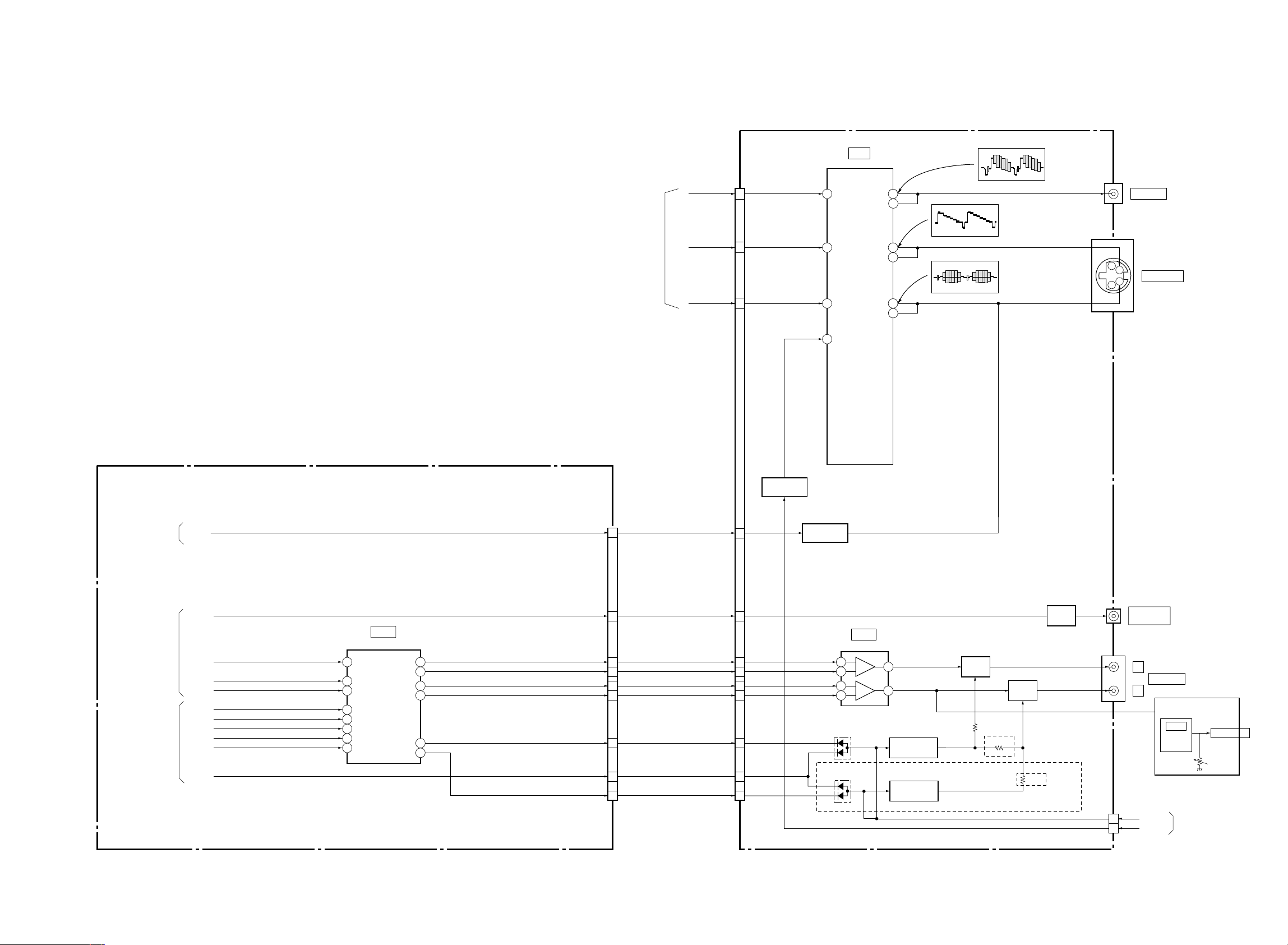
3-5. VIDEO/AUDIO BLOCK DIAGRAM
DVP-PQ2
SIGNAL
PROCESSOR
(SEE PAGE 3-6)
AV-77 BOARD
(SEE PAGE 4-23)
CN100
V
Y
C
15
19
17
VIDEO BUFFER
INA
2
INC
7
INB
4
MUTE
1
IC101
OUTA1
OUTA2
OUTC2
OUTB1
OUTB2
15
14
10OUTC1
9
13
12
IC101 q;
2.0 Vp-p (H)
IC101 qd
1.8 Vp-p (H)
IC101 qg
2.4 Vp-p (H)
J201 (1/3)
J100
Y
C
VIDEO OUT
S-VIDEO OUT
MB-108 BOARD (5/5)
(SEE PAGE 4-19)
SYSTEM
CONTROL
(SEE PAGE 3-8)
SIGNAL PROCESSOR
(SEE PAGE 3-6)
SYSTEM
CONTROL
(SEE PAGE 3-8)
WIDE
SPDIF
ACH12
BCK
LRCK
512FS2CH
XDACS
XRST
SC1
SO1
MAMUTE
IC601
AUDIO D/A CONVERTER
3
SDTI AOUTL+
BICK2
LRCK4
MCLK1
CSN6
PDN5
CCLK7
CDTI8
AOUTL–
AOUTR+
AOUTR–
DZFL
DZFR
Q109
MUTE DRIVE
CN601
12
16
12
11
10
9
17
15
21
23
SPDIF
ALT+
ALT–
ART+
ART–
14
10
9
11
5
3
Q104, 105
WIDE SWITCH
AUDIO AMP
5
6
3
2
IC202
+
–
+
–
J201 (3/3)
Q200
BUFFER
J201 (2/3)
7
1
Q208
MUTE
Q207
MUTE
DIGITAL OUT
(COAXIAL)
L
AUDIO OUT
R
HP-137 BOARD
(PQ2: U2,MX2,
16
15
22
24
20
LMUTE
MAMUTE
RMUTE
4
2
6
D201
D202
(PQ2: EC1,EC2,CEK)
Q201, 202, 203
MUTE DRIVE
(PQ2: EC1,EC2,CEK)
Q204, 205, 206
MUTE DRIVE
R247
CA2)
R246
(PQ2: EC1,EC2,CEK)
R245
CN301
5
6 VMUTE
A MUTE
IC501
AUDIO
AMP
INTERFACE
CONTROL
(SEE PAGE 3-11)
0
J501
RV501
05
3-9 3-10
Page 26

DVP-PQ2
3-6. INTERFACE CONTROL BLOCK DIAGRAM
SYSTEM CONTROL
(SEE PAGE 3-8)
VIDEO/AUDIO
(SEE PAGE 3-10)
SO0
SC0
XIFCS
XIFBUSY
XFRRST
A MUTE
VMUTE
SI0
IF-106 BOARD
(SEE PAGE 4-29)
CN807
4
1
3
6
5
8
CN810
5
6
SI0
SO0
SC0
XIFCS
XIFBUSY
XFRRST
25
24
26
20
19
18
17
16
R91 (SO)
R90 (SI)
R92 (SCK)
R80 (INT2)
R63
R62
R61
R60
IC804
IF CON
R40 (AIN0)
R41 (AIN1)
R70
R51 (AIN5)
R50 (AIN4)
SW-407 BOARD
(SEE PAGE 4-34)
1
2
CN950
S950
S951
S950, 951
COVER
OPEN/CLOSE
DETECT
CN812
7
8
4
12
11
13R52 (AIN6)
10R43 (AIN3)
15R53 (AIN7)
22R82 (INT1/ZIN)
CN811
SW+5V
1
2
9
8
7
6
5
4
1
SW-406 BOARD
(SEE PAGE 4-33)
CN901
1
SW+5V
2
3
4
5
6
9
Q900
LED DRIVE
D901
I/1
S900
H
S901
x
S902
.
S903
I/1
S904
>
IC900
REMOTE COMMANDER
RECEIVER
1
VOUT
P-CONT
XIN
XOUT
2
1
IC800
RESET
3
VOUT
4
05
RESET
X800
8MHz
POWER 1
(SEE PAGE 3-14)
IC804 1
3.4 Vp-p (8 MHz)
3-11 3-12
Page 27

3-7. POWER 1 BLOCK DIAGRAM
10
4
•
5
J2
F101
T1
D401
D101
D301
D1A-1D
AC IN
F1
J1
05
IF-106 BOARD
(SEE PAGE 4-29)
POWER 2
(SEE PAGE 3-15)
POWER 2
(SEE PAGE 3-15)
D201
D303
IC2
PHOTO COUPLER
SWITCHING
CONTROL
6
9
1
11
1
2
Q401
Q101
Q301
FL1, 2
LINE
FILTER
D411
F301
Q402
POWER
CONTROL
L401
L410
L101
L301
IC804
IF CON
IC800
RESET
IC302 , Q302
IC303
IC1
SHUNT REG
IC801
+1.8V REG
9 R42 (AIN2)
EVER+3.3V
EVER+3.3V
EVER+3.3V
AI+5V
+3.3V
+5V
+1.8V
SW+11V
L802
+11V
3.3V MNT
AU+11V
PS801
1
VIN
3VOUT
CN801
2
CN809
CN807
CN901
EVER +3.3V
3
3
11
9
10
6 4
1
5
7
2
CN810
4
1
1
4
•
5
SW+11V
+11V (AUDIO)
+5V
SW+3.3V
EVER+3.3V
P-CONT
+3.3V REG
IC900
REMOTE
COMMANDER
RECEIVER
D901
I/1
SW-406 BOARD
(SEE PAGE 4-33)
F401
(PQ2: U2,CA2,MX2)
Q1
INTERFACE
CONTROL
(SEE PAGE 3-11)
SWITCHING REGULATOR
DPSN-20CP (PQ2: U2,CA2,MX2)
DPSN-20CP-2 (PQ2: EC1,EC2,CEK)
(SEE PAGE 4-41, 4-45)
( )
(PQ2: EC1,EC2,CEK)
DVP-PQ2
3-13 3-14
Page 28

DVP-PQ2
3-8. POWER 2 BLOCK DIAGRAM
AV-77 BOARD
(SEE PAGE 4-23)
POWER 1
(SEE PAGE 3-14)
AI+5V
AU+11V
EVER+3.3V
1
2
4
1
CN301
CN100
Q292
L201
D200
3
L103
+5V REG
IN
MUTE V
IC200
IC101
VIDEO
BUFFER
IC202
AUDIO AMP
1OUT
HP-137 BOARD
7
6
7
IC501
AUDIO AMP
6
8
POWER 1
(SEE PAGE 3-14)
3.3V MNT
+3.3V
+5V
+1.8V
+11V
AU+5V
MB-108 BOARD
(SEE PAGE 4-9 to 4-20)
CN601
25
CN101
7
CN102
4
2
1
5
FL110
FILTER
FL105
FILTER
FL104
FILTER
FL109
FILTER
IC601
AUDIO
D/A CONVERTER
IC202
FOCUS/TRACKING
COIL DRIVE,
SPINDLE/SLED/
LOADING
MOTOR DRIVE
FL106
FILTER
FL101
FILTER
IC107
16M FLASH
IC103
PLL
IC108
or
OTP
IC201
DVD/CD RF AMP,
DIGITAL
SERVO
FL103
FILTER
FL102
FILTER
IC101
EEPROM
IC104
SYSTEM
CONTROL
IC303
16M DRAM
FL404
FILTER
2
IC302
+3.3V REG
VIN
IC404
16M SDRAM
IC405
16M SDRAM
1VOUT
5
IC301
ARP,
SERVO DSP
IC402
+3.3V REG
VIN
+1.8V REG
5
VIN
IC401
FL402
FILTER
FL403
FILTER
4VOUT
4VOUT
IC403
AV DECODER
FL201
FILTER
CN204
5
CN203
19
11
LED
VCC
MOD
INLIMIT
SENSOR
OPTICAL
DEVICE
05
3-15 3-16E
Page 29

SECTION 4
PRINTED WIRING BOARDS AND SCHEMATIC DIAGRAMS
4-1. PRINTED WIRING BOARDS AND SCHEMA TIC DIAGRAMS
THIS NOTE IS COMMON FOR WIRING BOARDS AND SCHEMATIC DIAGRAMS
(In addition to this, the necessary note is printed in each block)
DVP-PQ2
For printed wiring boards
• : indicates a lead wire mounted on the component side.
• : indicates a lead wire mounted on the printed side.
• a : Through hole.
•
• Abbreviation
: Pattern from the side which enables seeing.
(The other layers' patterns are not indicated.)
Caution:
Pattern face side: Parts on the pattern face side seen from
(Side B) the pattern face are indicated.
Parts face side: Parts on the parts face side seen from
(Side A) the parts face are indicated.
U2 : United States model
CA2 : Canada model
MX2 : Mexico model
EC1 : Europe model
EC2 : Europe model
CEK : United Kingdom model
(For schematic diagrams)
• All capacitors are in mF unless otherwise noted. pF : mmF.
50V or less are not indicated except for electrolytics and
tantalums.
• All resistors are in ohms, 1/4W (Chip resistors : 1/10W) un-less
otherwise specified.
kW = 1000W, MW = 1000kW.
• Caution when replacing chip parts.
New parts must be attached after removal of chip.
Be careful not to heat the minus side of tantalum capacitor,
because it is damaged by the heat.
• All variable and adjustable resistors have characteristic curve
B, unless otherwise noted.
•
•
• : panel designation
• f : internal component.
• : adjustment for repair.
• : B+ Line
•
• Circled numbers refer to waveforms.
• Voltages are dc between measurement point.
• Readings are taken with a color-bar signals on DVD reference
• Readings are taken with a digital multimeter (DC 10MW).
• Voltage variations may be noted due to normal production tol-
: non flammable resistor
: fusible resistor
B +
: B– Line
B –
disc and when playing CD reference disc.
erances.
Note :
The components identified by
mark or dotted line with mark
are critical for safety.
Replace only with part number
specified.
Note :
Les composants identifiés par
une marque sont critiques
pour la sécurité.
Ne les remplacer que par une
pièce portant le numéro spécifié.
When indicating parts by reference number, please include
the board name.
4-1 4-2
Page 30

DVP-PQ2
4-2. FRAME SCHEMATIC DIAGRAM
FRAME SCHEMA TIC DIAGRAM
4-44-3
Page 31

MB-108 BOARD
A V-077 BOARD IF-106 BOARD
1
IC103 3
2
IC103 8
3
IC103 9 q;
4
IC103 qg
1.17msec
38nsec
42nsec
3.3Vp-p
3.3Vp-p
3.3Vp-p
7
IC201 ra (DVD PLAY)
8
IC201 rs (CD PB)
8
IC201 rs (DVD PLAY)
9
IC201 tl
1.7Vp-p
383mVp-p
433mVp-p
125
13
IC301 (CD PB)
21msec
125
13
IC301 (DVD PLAY)
32.4msec
150 158 160
14
IC301
30nsec
15
IC403 ws
770mVp-p
466mVp-p
1.1Vp-p
20
21
22
32
IC403 yd
6.8usec
IC403 yg
33.5usec
IC403
IC601 1
38nsec
625mVp-p
1.1Vp-p
3.3Vp-p
1
2
3
IC101 q;
IC101 qd
H
IC101 qg
H
1 IC404 2
2.0Vp-p
H
8 MHz
1.8Vp-p
2.4Vp-p
3.4Vp-p
30nsec
5
IC104 tf
60nsec
6
IC201 2 (CD PB)
20nsec
6
IC201 2 (DVD PLAY)
20nsec
7
IC201 ra (CD PB)
3.3Vp-p
3.3Vp-p
0.47Vp-p
0.79Vp-p
890nsec
111
10
IC301 (DVD PLAY)
40ns/div
113
11
IC301 (CD PB)
0.2us/div
124
12
IC301 (CD PB)
1.8msec
12
124
IC301 (DVD PLAY)
1.3Vp-p
1.34Vp-p
1.46Vp-p
1.5Vp-p
16
17
18
19
IC403 tg
63.5usec
IC403 tj
63.5usec
IC403 tl
63.5usec
IC403 ya
40nsec
3.3Vp-p
1.0Vp-p
979mVp-p
675mVp-p
42nsec
3.3Vp-p
1.6Vp-p
1.0msec
1.62Vp-p
6.35usec
666mVp-p
WAVEFORMS
MB-108/AV-077/IF-106
4-5 4-6
Page 32

DVP-PQ2
SW-406
(FUNCTION SWITCH)
SW-407
(DOOR SWITCH)
AV-77
(AUDIO/VIDEO OUT)
IF-106
(INTERFACE CONTROL)
HP-137
(HEADPHONE)
MB-108
(SIGNAL PROCESS, SERVO)
SWITCHING REGULATOR
DPSN-20CP (PQ2: U2,CA2,MX2)
DPSN-20CP-2 (PQ2: EC1,EC2,CEK)
MB-108 (DVD/CD RF AMP,DIGIT AL SERVO,MOT OR DRIVE,SERVO,A V DECODER,SD RAM,
SYSTEM CONTROL,AUDIO DAC,PLL) PRINTED WIRING BOARD
MB-108 BOARD (SIDE A)
• : Uses unleaded solder.
MB-108 BOARD (SIDE B)
MB-108 BOARD
A SIDE
IC104 B-6
IC301 B-3
IC302 B-2
IC402 D-6
IC403 C-5
IC501 C-2
IC502 C-5
IC601 D-3
DVD/CD RF AMP,DIGITAL SERVO,MOTOR DRIVE,SER VO,A V DECODER,SD RAM, SYSTEM CONTROL,AUDIO DAC,PLL
B SIDE
IC101 A-5
IC103 C-4
IC106 B-6
IC107 B-5
IC108 B-4
IC201 C-1
IC202 B-1
IC303 B-3
IC401 B-4
IC404 C-4
IC405 C-5
IC406 C-5
IC503 D-2
IC504 C-5
IC505 D-3
Q201 D-1
Q202 D-1
D201 D-1
D202 D-1
For printed wiring board
There are a few cases that the part printed on
this diagram isn’t mounted in this model.
MB-108
4-8
Page 33

For Schematic Diagram
1
2
3
4
5
• Refer to page 4-7 for printed wiring board of MB-108 board.
• Refer to page 4-5 for waveform
• Refer to page 4-17 differential Part List
1
MB-108 BOARD (1/5)
SYSTEM CONTROL
A
-REF.NO.:1000 SERIESXX MARK:NO MOUNT
NO MARK:REC/PB MODE
2
B
C
DVP-PQ2
43
98765
10
11
12
13
14
15
D
E
F
G
H
I
The components identified by
mark
mark are critical for safety.
Replace only with part
J
number specified.
or dotted line with
4-9 4-10
Les composants identifiés par
une marque
pour la sécurité . Ne les
remplacer que par une pièce
portant le numéro spécifié.
sont critiques
SYSTEM CONTROL
MB-108 (1/5)
Page 34

DVP-PQ2
VIDEO SIGNAL
CHROMAPBY Y/CHROMA
AUDIO
SIGNAL
SIGNAL PATH
SPINDLE SERVO (SPEED AND PHASE)
TRACKING SERVO DVD/CD CDV
SLED SERVO DVD/CD
FOCUS SERVO
SKEW SERVO DVD/CD
For Schematic Diagram
• Refer to page 4-7 for printed wiring board of MB-108 board.
• Refer to page 4-5 for waveform
• Refer to page 4-17 differential Part List
1
MB-108 BOARD (2/5)
MOTOR DRIVE
A
-REF.NO.:2000 SERIESXX MARK:NO MOUNT
NO MARK:PB MODE
2
43
98765
10
11
12
13
14
15
B
C
D
E
0
2.0
2.0
2.0
5.0
2.4
3.2
3.2
2.0
2.0
2.0
2.0
2.0
2.0
2.0
0
2.0
2.0
2.0
2.0
2.0
2.0
2.0
2.0
0.01
3.4
3.400
3.4
3.4
5.3
5.3
3.4
11.0
5.3
5.3
5.3
-0.05
5.2
5.4
0
5.3
5.3
5.0
6.0
-0.05
5.3
3.4
3.4
11.0
5.3
F
G
H
I
J
9
3.4
1.0
3.2
3.002.2
2.2
3.2
3.2
2.3
3.0
5.0
4.0
4.0
4.0
6
4.0
3.2
3.0
4.0
3.2
3.2
0
2.0
0
3.3
0.03
0.03
0.02
2.5
0.03
2.4
0.03
0.03
0.03
3.0
0.1
5.0
3.0
0
5.1
5.1
1.0
0.1
0.104.4
5.0
0
3.1
2.1
0.1
0
0.1
0.04
4.0
8
0.4
4.0
2.0
2.0
3.0
2.0
0.05
1.3
2.2
0.3
3.0
0.04
3.0
2.1
2.2
7
MOTOR DRIVE
MB-108 (2/5)
4-11 4-12
Page 35

For Schematic Diagram
0
0
0.1
0
1.2
0
2.0
1.0
1.0
3.0
3.4
3.4
0
0
2.0
0
0
0
3.4
2.0
0
2.0
0
3.1
2.0
3.4
3.4
3.4
3.2
3.1
2.0
2.0
0.1
3.2
3.2
3.1
3.2
3.2
3.4
3.1
3.0
3.1
2.4
3.0
0
3.2
3.2
3.1
3.2
3.1
3.2
3.2
2.0
3.4
2.0
2.0
3.4
3.003.4
3.4
3.0
3.4
0.3
0.1
0.3
0.2
0.4
0.5
0.3
0.2
0.2
0.202.0
1.3
3.0
0
0
2.0
3.0
2.0
0.5
2.0
2.002.0
3.1
0
2.0
1.0
2.4
3.3
0
2.0
2.0
2.0
-0.03
2.0
2.0
3.3
-0.04
0.5
0
3.3
0
1.0
0
3.4
3.0
2.0
3.3
2.0
0
1.0
0
3.4
0
3.4
0
0
0
0
2.0
2.0
0
2.0
2.2
0
0
1.0
0
3.4
2.0
2.1
1.4
1.1
1.4
1.0
1.0
2.0
3.4
2.000
2.0
0.102.0
2.001.503.4
3.400
3.4
3.4
3.0
3.4
3.4
3.403.30002.0
3.4
3.0
2.001.3
1.7
2.0
3.4
3.3
3.0
3.2
3.3
3.4
3.2
3.2
3.2
4.0
0
0
0
3.1
3.3
0
0
0.2
0.2
0.3
0.2
4.0
0.2
0.2
0.3
0.1
0.2
0.2
0
0
3.3
3.3
0
0
3.1
3.2
3.1
3.1
0
3.2
3.2
3.2
3.2
0
5.0 5.0
0
1.3 3.3
10
11
12
13
14
VIDEO SIGNAL
CHROMAPBY Y/CHROMA
AUDIO
SIGNAL
SIGNAL PATH
SPINDLE SERVO (SPEED AND PHASE)
TRACKING SERVO DVD/CD CDV
SLED SERVO DVD/CD
FOCUS SERVO
SKEW SERVO DVD/CD
• Refer to page 4-7 for printed wiring board of MB-108 board.
• Refer to page 4-5 for waveform
• Refer to page 4-17 differential Part List
1
2
MB-108 BOARD (3/5)
SERVO
A
-REF.NO.:3000 SERIESXX MARK:NO MOUNT
NO MARK:PB MODE
B
C
DVP-PQ2
43
98765
10
11
12
13
14
15
D
E
F
G
H
I
J
4-13 4-14
SERVO
MB-108 (3/5)
Page 36

DVP-PQ2
0
2.1
3.4
5.0
3.1
0
3.2
5.0
0
1.3
03.4
1.1
2.0
2.0
2.2
3.4
2.1
2.0
0
2.0
2.0
3.4
0.1
0.1
1.4
3.4
0.1
0.1
0.1
2.0
2.4
1.5
1.5
0
2.0
2.0
0
2.0
2.0
3.4
2.0
2.0
0
1.2
1.5
3.4
0.1
1.3
3.0
3.0
3.1
2.0
0.1
0.1
0.5
2.0
0.12
3.4
03.4
1.0
2.0
0
2.1
2.4
3.4
2.0
2.0
0
2.0
2.0
3.4
0.1
1.4
0.1
3.4
-0.05
0.1
0.1
2.0
1.2
1.5
1.5
0
2.0
2.0
0
2.0
1.4
3.4
2.0
1.5
0
1.0
2.0
3.4
0.1
3.1
3.0
3.0
3.1
1.0
0.1
0.1
1.0
2.0
1.0
3.4
0
0
0
4.3
3.4
0
2.1
2.2
3.4
2.0
1.0
0
1.0
1.0
0.5
2.1
3.4
2.0
1.1
1.0
1.1
1.3
1.0
1.2
2.3
1.3
0
0.1
0.1
0
3.3
3.0
0
0
0
3.0
3.4
4.0
3.3
3.3
2.0
0
0.03
0
0.3
0.04
4.0
0.1
2.4
0.3
3.0
0
3.3
1.0
1.3
0
1.0
1.0
1.4
1.2
0
2.0
1.0
1.0
1.3
2.0
2.0
2.0
2.0
0
0
2.0
1.0
1.0
2.0
0
2.0
2.0
0
0
0
3.4
2.0
2.0
2.0
2.0
0
0
2.0
2.0
3.4
3.4
0
0
3.4
3.4
0
0
0
3.4
2.0
2.0
4.0
4.0
3.4
3.4
0.1
0.1
2
.1
2
.0
2
.0
2
.0
1
.1
1
.0
0
1
.0
0
0
2
.0
0
.5
1
.2
0
0
2
.0
3
.4
1
.2
2
.1
2
.0
2
.0
3
.2
3
.4
3
.4
3
.1
3
.4
3
.4
0
3
.4
3
.4
3
.4
3
.4
1
.0
1
.0
0
.2
0
2
.0
2
.1
0
2
.4
1
.0
3
.4
3
.4
4
.0
0
0
0
0
2
.0
2
.0
2
.0
0
3.3
0.300.3
3.3
1.001.0
3.3
2.000.303.4
2.0
3.3
0.4
0.4
4.0
2.0
3.20002.00004.0
4.002.0
1.0
1.2
2.0
2.0
2.0
1.1
1.1
3.0
2.0
3.102.0
3.103.3
3.000
0
16
171918 20
21
15
22
For Schematic Diagram
• Refer to page 4-7 for printed wiring board of MB-108 board.
• Refer to page 4-5 for waveform
• Refer to page 4-17 differential Part List
1
MB-108 BOARD (4/5)
AV DECODER
A
-REF.NO.:4000 SERIESXX MARK:NO MOUNT
NO MARK:PB MODE
B
C
D
E
F
G
2
43
98765
10
11
12
13
14
15
H
I
J
A V DECODER
MB-108 (4/5)
SIGNAL PATH
VIDEO SIGNAL
CHROMAPBY Y/CHROMA
AUDIO
SIGNAL
4-15 4-16
Page 37

For Schematic Diagram
• Refer to page 4-7 for printed wiring board of MB-108 board.
• Refer to page 4-5 for waveform
• Refer to page 4-17 differential Part List
MB-108 BOARD (5/5)
AUDIO DAC, PLL
-REF.NO.:6000 SERIESXX MARK:NO MOUNT
NO MARK:PB MODE
DVP-PQ2
1
2.0
2.0
1.2
2.0
3.4
3.4
3.4
0
5.0
5.0
5.0
0
2.4
2.4
2.4
2.4
MB-108 BOARD differential Part List (1/5-5/5)
PQ2: U2 PQ2: CA2 PQ2: MX2 PQ2: EC1 PQ2: EC2 PQ2: CEK
C441 XX XX XX 0.01 25V :CHIP 0.01 25V :CHIP 0.01 25V :CHIP
C442 XX XX XX 0.01 25V :CHIP 0.01 25V :CHIP 0.01 25V :CHIP
C447 XX XX XX 0.01 25V :CHIP 0.01 25V :CHIP 0.01 25V :CHIP
IC405 XX XX XX HY57V161610DTC-7TR HY57V161610DTC-7TR HY57V161610DTC-7TR
R164 XX XX 220 : CHIP 12K : CHIP 12K : CHIP 12K : CHIP
R169 XX XX 12K : CHIP 47K : CHIP 47K : CHIP 47K : CHIP
TO AF-98 BOARD
CN203 (PAGE )
4-17 4-18
AUDIO DAC, PLL
MB-108 (5/5)
Page 38

DVP-PQ2
SW-406
(FUNCTION SWITCH)
SW-407
(DOOR SWITCH)
AV-77
(AUDIO/VIDEO OUT)
IF-106
(INTERFACE CONTROL)
HP-137
(HEADPHONE)
MB-108
(SIGNAL PROCESS, SERVO)
SWITCHING REGULATOR
DPSN-20CP (PQ2: U2,CA2,MX2)
DPSN-20CP-2 (PQ2: EC1,EC2,CEK)
A V -77 (AUDIO/VIDEO OUT) PRINTED WIRING BOARD
A V-77 BOARD (SIDE A)
C
B
A
12345
A V -77 BOARD (SIDE B)
C
B
• : Uses unleaded solder.
For printed wiring board
There are a few cases that the part printed on
this diagram isn’t mounted in this model.
AV -77 BOARD
B SIDE
IC200 B-3
IC202 A-3
IC401 C-4
D103 B-5
D104 B-5
D200 C-1
D201 C-2
D202 C-2
D205 B-3
D206 B-4
D291 B-1
Q104 C-4
Q105 C-4
Q109 C-4
Q200 B-4
Q201 A-1
Q202 A-1
Q203 A-1
Q204 A-1
Q205 A-1
Q206 B-1
Q207 A-4
Q208 A-4
Q291 B-1
Q292 C-2
Q294 C-1
A
AUDIO/VIDEO OUT
12345
AV-77
4-19
4-20
Page 39

For Schematic Diagram
• Refer to page 4-19 for printed wiring board of AV-77 board.
• Refer to page 4-5 for waveform
• Refer to page 4-23 differential Part List
1
AV-77
AUDIO/VIDEO OUT
A
-REF.NO.:6000 SERIESXX MARK:NO MOUNT
NO MARK:PB MODE
2
B
C
DVP-PQ2
43
98765
10
11
12
13
14
15
D
E
F
G
H
I
SIGNAL PATH
CHROMAPBY Y/CHROMA
VIDEO SIGNAL
AUDIO
SIGNAL
J
AUDIO/VIDEO OUT
AV-77
4-21
4-22
Page 40

DVP-PQ2
A V -77 BOARD differential Part List
PQ2: U2 PQ2: CA2 PQ2: MX2 PQ2: EC1 PQ2: EC2 PQ2: CEK
C234 XX XX XX 1 1 1
C237 XX XX XX 220P : CHIP 220P : CHIP 220P : CHIP
C238 XX XX XX 220P : CHIP 220P : CHIP 220P : CHIP
D202 XX XX XX DAP202K-T146 DAP202K-T146 DAP202K-T146
Q204 XX XX XX UN2213-TX UN2213-TX UN2213-TX
Q205 XX XX XX DTC124TKA-T146 DTC124TKA-T146 DTC124TKA-T146
Q206 XX XX XX 2SB709A-QRS-TX 2SB709A-QRS-TX 2SB709A-QRS-TX
R215 XX XX XX 22K :CHIP 22K :CHIP 22K :CHIP
R235 XX XX XX 10K :CHIP 10K :CHIP 10K :CHIP
R236 XX XX XX 10K :CHIP 10K :CHIP 10K :CHIP
R237 XX XX XX 47K :CHIP 47K :CHIP 47K :CHIP
R242 XX XX XX 10K : CHIP 10K : CHIP 10K : CHIP
R245 XX XX XX 4.7K :CHIP 4.7K :CHIP 4.7K :CHIP
R246 4.7K : CHIP 4.7K : CHIP 4.7K : CHIP XX XX XX
R280 0 :CHIP 0 :CHIP 0 :CHIP XX XX XX
R297 XX XX XX 0 :CHIP 0 :CHIP 0 :CHIP
4-23 4-24
Page 41

DVP-PQ2
SW-406
(FUNCTION SWITCH)
SW-407
(DOOR SWITCH)
AV-77
(AUDIO/VIDEO OUT)
IF-106
(INTERFACE CONTROL)
HP-137
(HEADPHONE)
MB-108
(SIGNAL PROCESS, SERVO)
SWITCHING REGULATOR
DPSN-20CP (PQ2: U2,CA2,MX2)
DPSN-20CP-2 (PQ2: EC1,EC2,CEK)
IF-106 (INTERFACE CONTROL) PRINTED WIRING BOARD
IF-106 BOARD (SIDE A)
D
C
B
A
• : Uses unleaded solder.
For printed wiring board
There are a few cases that the part printed on
this diagram isn’t mounted in this model.
IF-106 BOARD
B SIDE
IC801 B-2
IC804 C-2
123
IF-106 BOARD (SIDE B)
D
C
B
A
123
INTERF ACE CONTROL
IF-106
4-25 4-26
Page 42

DVP-PQ2
For Schematic Diagram
• Refer to page 4-25 for printed wiring board of IF-106 board.
• Refer to page 4-5 for waveform
1
IF-106
INTERFACE CONTROL
A
-REF.NO.:6000 SERIESXX MARK:NO MOUNT
NO MARK:PB MODE
B
C
2
43
98765
10
11
12
13
14
15
D
E
F
G
H
IF-106 BOARD differential Part List
PQ2: U2 PQ2: CA2 PQ2: MX2 PQ2: EC1 PQ2: EC2 PQ2: CEK
C807 220P :CHIP 220P :CHIP 220P :CHIP 0.1 :CHIP 0.1 :CHIP 0.1 :CHIP
C808 0.01 :CHIP 0.01 :CHIP 0.01 :CHIP 0.1 :CHIP 0.1 :CHIP 0.1 :CHIP
C810 0.01 :CHIP 0.01 :CHIP 0.01 :CHIP 0.1 :CHIP 0.1 :CHIP 0.1 :CHIP
C811 0.001 :CHIP 0.001 :CHIP 0.001 :CHIP 0.1 :CHIP 0.1 :CHIP 0.1 :CHIP
I
C813 # # # 0.1 :CHIP 0.1 :CHIP 0.1 :CHIP
C815 # # # 0.1 :CHIP 0.1 :CHIP 0.1 :CHIP
C829 # # # 0.1 :CHIP 0.1 :CHIP 0.1 :CHIP
R825 0 :CHIP 0 :CHIP 0 :CHIP # # #
J
INTERF ACE CONTROL
IF-106
4-27
4-28
Page 43

SW-406 (FUNCTION SWITCH) PRINTED WIRING BOARD
123
A
123
A
SW-406
(FUNCTION SWITCH)
SW-407
(DOOR SWITCH)
AV-77
(AUDIO/VIDEO OUT)
IF-106
(INTERFACE CONTROL)
HP-137
(HEADPHONE)
MB-108
(SIGNAL PROCESS, SERVO)
SWITCHING REGULATOR
DPSN-20CP (PQ2: U2,CA2,MX2)
DPSN-20CP-2 (PQ2: EC1,EC2,CEK)
SW-407 (DOOR SWITCH) PRINTED WIRING BOARDS
SW-406 BOARD (SIDE A)
B
A
123456
SW-406 BOARD (SIDE B)
SW-406 BOARD (SIDE A)
SW-406 BOARD (SIDE B)
• : Uses unleaded solder.
For printed wiring board
B
A
123456
There are a few cases that the part printed on
this diagram isn’t mounted in this model.
SW-406 BOARD
A SIDE
IC900 B-3
D901 B-3
B SIDE
D900 B-4
Q900 B-4
FUNCTION SWITCH
SW-406
DOOR SWITCH
/
SW-407
4-29 4-30
Page 44

DVP-PQ2
For Schematic Diagram
• Refer to page 4-29 for printed wiring board of SW-406, SW-407 boards.
1
2
43
98765
10
11
12
13
14
15
A
B
C
D
SW-406
FUNCTION SWITCH
-REF.NO.:6000 SERIESXX MARK:NO MOUNT
NO MARK:PB MODE
SW-407
DOOR SWITCH
-REF.NO.:6000 SERIESXX MARK:NO MOUNT
NO MARK:PB MODE
E
F
G
H
SW-406 BOARD differential Part List
PQ2: U2 PQ2: CA2 PQ2: MX2 PQ2: EC1 PQ2: EC2 PQ2: CEK
C903 # # # 0.1 :CHIP 0.1 :CHIP 0.1 :CHIP
SW-407 BOARD differential Part List
PQ2: U2 PQ2: CA2 PQ2: MX2 PQ2: EC1 PQ2: EC2 PQ2: CEK
W901 # # # HARNESS(LG-50) HARNESS(LG-50) HARNESS(LG-50)
I
J
FUNCTION SWITCH
SW-406
DOOR SWITCH
/
SW-407
4-324-31
Page 45

DVP-PQ2
SW-406
(FUNCTION SWITCH)
SW-407
(DOOR SWITCH)
AV-77
(AUDIO/VIDEO OUT)
IF-106
(INTERFACE CONTROL)
HP-137
(HEADPHONE)
MB-108
(SIGNAL PROCESS, SERVO)
SWITCHING REGULATOR
DPSN-20CP (PQ2: U2,CA2,MX2)
DPSN-20CP-2 (PQ2: EC1,EC2,CEK)
HP-137 (HEADPHONE) PRINTED WIRING BOARD
HP-137 BOARD (SIDE A)
B
A
12345
HP-137 BOARD (SIDE B)
B
• : Uses unleaded solder.
For printed wiring board
There are a few cases that the part printed on
this diagram isn’t mounted in this model.
HP-137 BOARD
B SIDE
IC501 A-3
D501 A-1
D502 A-1
Q501 A-3
Q502 A-3
A
12345
4-33 4-34
HEADPHONE
HP-137
Page 46

DVP-PQ2
For Schematic Diagram
• Refer to page 4-35 for printed wiring board of HP-137 board.
1
HP-137
HEADPHONE
A
-REF.NO.:6000 SERIESXX MARK:NO MOUNT
NO MARK:PB MODE
B
C
2
43
98765
10
11
12
13
14
15
D
E
F
G
H
I
J
HEADPHONE
HP-137
4-35 4-36
Page 47

DVP-PQ2
SW-406
(FUNCTION SWITCH)
SW-407
(DOOR SWITCH)
AV-77
(AUDIO/VIDEO OUT)
IF-106
(INTERFACE CONTROL)
HP-137
(HEADPHONE)
MB-108
(SIGNAL PROCESS, SERVO)
SWITCHING REGULATOR
DPSN-20CP (PQ2: U2,CA2,MX2)
DPSN-20CP-2 (PQ2: EC1,EC2,CEK)
DPSN-20CP (SWITCHING REGULA T OR) PRINTED WIRING BOARD
(PQ2: U2,CA2,MX2)
DPSN-20CP BOARD
• : Uses unleaded solder.
For printed wiring board
There are a few cases that the part printed on
this diagram isn’t mounted in this model.
1-468-694-12
SWITCHING REGULA TOR
DPSN-20CP
4-37 4-38
Page 48

DVP-PQ2
For Schematic Diagram
• Refer to page 4-37 for printed wiring board of DPSN-20CP board.
1
DPSN-20CP (PQ2: U2,CA2,MX2)
SWITCHING REGULATOR
A
-REF.NO.:6000 SERIESXX MARK:NO MOUNT
NO MARK:PB MODE
B
C
2
43
98765
10
11
12
13
14
15
D
E
F
G
H
I
J
SWITCHING REGULA TOR
DPSN-20CP
4-39 4-40
Page 49

DVP-PQ2
SW-406
(FUNCTION SWITCH)
SW-407
(DOOR SWITCH)
AV-77
(AUDIO/VIDEO OUT)
IF-106
(INTERFACE CONTROL)
HP-137
(HEADPHONE)
MB-108
(SIGNAL PROCESS, SERVO)
SWITCHING REGULATOR
DPSN-20CP (PQ2: U2,CA2,MX2)
DPSN-20CP-2 (PQ2: EC1,EC2,CEK)
DPSN-20CP-2 (SWITCHING REGULAT OR) PRINTED WIRING BOARD
(PQ2: EC1,EC2,CEK)
DPSN-20CP-2 BOARD
• : Uses unleaded solder.
For printed wiring board
There are a few cases that the part printed on
this diagram isn’t mounted in this model.
1-468-694-22
SWITCHING REGULA TOR
DPSN-20CP-2
4-41 4-42
Page 50

DVP-PQ2
For Schematic Diagram
• Refer to page 4-41 for printed wiring board of DPSN-20CP-2 board.
1
DPSN-20CP-2 (PQ2: EC1,EC2, CEK)
SWITCHING REGULATOR
A
-REF.NO.:6000 SERIESXX MARK:NO MOUNT
NO MARK:PB MODE
B
C
2
43
98765
10
11
12
13
14
15
D
E
F
G
H
I
J
SWITCHING REGULA TOR
DPSN-20CP-2
4-43 4-44E
Page 51

SECTION 5
IC PIN FUNCTION DESCRIPTION
5-1. SYSTEM CONTROL PIN FUNCTION
(MB-108 BOARD IC104: MB91307RPFV -G-BND-E1)
Pin No. Pin name I/O Function
1-5 HA17-HA21 O Address bus A17-A21
6 HA22 - Not used
7 WP O I2C EEPROM write protect output
8 XSACS - Not used
9 AVCC - Power supply (+3.3 V)
10 AVRH - Reference power supply (+3.3 V)
11 AVSS - Ground
12 AN0 I Set of mode 0
13 AN1 I Set of mode 1
14 AN2 I Set of mode 2
15 AN3 I S101 interrupt
16 INT0 I AV DEC Interrupt input
17 INT1 I ARP Interrupt input
18 INT2 I SDSP Interrupt input
19 INT3 - Not used
20 INT4 I IF CON Interrupt input
21 INT5 - Not used
22 INT6 - Not used
23 INT7 - Not used
24 VCC - Power supply (+3.3 V)
25 SI0 I Serial bus 0 (data input)
26 SO0 O Serial bus 0 (data output)
27 SC0 O Serial bus 0 (clock output)
28 SI1 - Not used
29 SO1 O Serial bus 1 (data output)
30 SC1 O Serial bus 1 (clock output)
31 SI2 I Serial bus 2 (data input)
32 SO2 O Serial bus 2 (data output)
33 DSENS - Not used
34 VSS - Ground
35 XRST O System reset signal output
36 XARPRST O WIDE Select signal output
37 RGBSEL - Not used
38 SDA I/O I2C data input/output
39 SCL O I2C clock output
40 TRM+ - Not used
41 EUROV - Euro Video Signal
42 EXT/DSEL O I/P select signal output
43 MD0 I Input of mode select 0 (fixed at “ H”)
44 MD1 I Input of mode select 1 (fixed at “ L”)
45 MD2 I Input of mode select 2 (fixed at “ L”)
46 DREQ0 I AV DEC DMA-REQ 0 input
47 DACK0 O AV DEC DMA-ACK 0 output
48 XDRVMUTE O Drive mute signal output
49 DREQ1 I AV DEC DMA-REQ 1 input
50 DACK1 O AV DEC DMA-ACK 1 output
51 XIFCS O IF CON Chip select signal output
52 VSS - Ground
53 X1 O Clock output (16.5 MHz)
54 X2 I Clock input (16.5 MHz)
DVP-PQ2
5-1
Page 52

Pin No. Pin name I/O Function
55 VCC - Power supply (+3.3 V)
56 CKSW1 - Not used
57 OCSW1 - Not used
58 CS0X O External ROM chip select signal output
59 CS1X O Extranal RAM chip select signal output
60 CS2X O AV DEC Chip select signal output
61 CS3X O AV DEC Chip select signal output
62 CS4X O ARP Chip select signal output
63 CS5X O SDSP Chip select signal output
64 VCCI - Power supply (+1.8 V)
65 CS6X - Not used
66 CS7X - Not used
67 XWAIT I Wait signal input
68 BGRNTX I Test terminal (fixed at “H”)
69 BRQ I Test terminal (fixed at “L”)
70 XRD O Read enable signal output
71 XWRH O High byte write enable signal output (16 bit and 8 bit)
72 XWRL O Lower order (progre only)
73 NMIX I Not used (fixed at “H”)
74 VCCI - Power supply (+1.8 V)
75 VSS - Ground
76 XFRRST I IF CON Reset signal input
77 CPUCK O CPU clock signal output
78 OCSW2 - Not used
79 XDACS O DAC (2ch) chip select signal output
80 TRM– - Not used
81 48/44.1K O PLL FS control signal output
82 WIDE O Laser diode mute signal output
83 MA_MUTE O Audio mute signal output
84 SRAMWE O SRAM write enable (progre only)
85-92 HD0-HD7 I/O Data bus D0-D7 (16 bit only)
93-100 HD8-HD15 I/O Data bus D8-D15 (16 bit) , D0-D7 (8 bit)
101 VSS - Ground
102-109 HA0-HA7 O Address bus A00-A07
110 VCC - Power supply (+3.3 V)
111-118 HA8-HA15 O Address bus A08-A15
119 VSS - Ground
120 HA16 O Address bus A16
5-2 E
Page 53

SECTION 6
TEST MODE
DVP-PQ2
6-1. GENERAL DESCRIPTION
The Test Mode allows you to make diagnosis and adjustment easily using the remote commander and monitor TV. The instructions,
diagnostic results, etc. are given on the on-screen display (OSD).
Note: Since the remote commander belongs to this model has no
number buttons, use other DVD remote commander with
number buttons on it.
6-2. ST ARTING TEST MODE
Press the [TOP MENU], [CLEAR], [I/ ] keys on the remote com-
mander in this order with the power of main unit in OFF status,
and the Test Mode starts, and the menu shown below will be displayed on the TV screen. At the bottom of menu screen, the model
name and revision number are displayed. Last Off at the lower
right of screen indicates the information code concerning the last
power off.
To execute each function, select the desired menu and press its
number on the remote commander.
To exit from the Test Mode, press the [I/ ] key.
Test Mode Menu
0. Syscon Diagnosis
1. Drive Auto Adjustment
2. Drive Manual Operation
3. ------
4. Emargency Hisory
5. Version Information
6. Video Level Adjustment
Exit: Power Key
_
Model:DPX-17xxxx
Revision:x.xxx Last Off: xx
Power Off Information Code List
1
1
6-3. SYSCON DIAGNOSIS
The same contents as board detail check by serial interface can be
checked from the remote commander.
On the Test Mode Menu screen, press
mander, and the following check menu will be displayed.
### Syscon Diagnosis ###
Check Menu
0. Quit
1. All
2. Version
3. Peripheral
4. Servo
5. Supply
6. AV Decoder
7. Video
8. Audio
_
0. Quit
Quit the Syscon Diagnosis and return to the Test Mode Menu.
1. All
All items continuous check
This menu checks all diagnostic items continuously. Normally, all
items are checked successively one after another automatically
unless an error is found, but at a certain item that requires judgment through a visual check to the result, the following screen is
displayed for the key entry.
### Syscon Diagnosis ###
Diag All Check
No. 2 Version
2-3. ROM Check Sum
Check Sum = xxxx
[0] key on the remote com-
00 : Primary Power Off
01 : Power Off Request from SYSTEM CONTROL
02 : Power Off by Emergency Power Off Command from SYS-
TEM CONTROL
(if information is sent from SYSTEM CONTROL)
03 : IF CON Judged that SYSTEM CONTROL is Faulty
04 : Power Off from Diagnosis Mode of IF CON
05 : Forced Power Off by the User
06 : Power Off by Power Supply Voltage Monitor
Press NEXT Key to Continue
Press PREV Key to Repeat
_
For the ROM Check, the check sum calculated by the Syscon is
output, and therefore you must compare it with the specified value
for confirmation.
Following the message, press > key to go to the next item,
or . key to repeat the same check again. To quit the diagnosis
and return to the Check Menu screen, press x or [ENTER] key.
If an error occurred, the diagnosis is suspended and the error code
is displayed as shown below.
### Syscon Diagnosis ###
3-3. EEPROM Check
Error 03: EEPROM Write/Read N
Address : 00000001
Write Data : 2492
Read Data : 2490
Press NEXT Key to Continue
Press PREV Key to Repeat
_
Press x key to quit the diagnosis, or . key to repeat the same
item where an error occurred, or > key to continue the check
from the item next to faulty item.
6-1
Page 54

Submenu
Selecting 2 and subsequent items calls the submenu screen of each
item.
Indication of “–” in the submenu means the check is not supported
with the model.
For example, if “5. Supply” is selected, the following submenu
will be displayed.
### Syscon Diagnosis ###
Check Menu
No. 5 Supply
0. Quit
1. All
2. ARP Register Check
3. ARP to RAM Data Bus
4. ARP to RAM Address Bus
5. ARP RAM Check
_
0. Quit
Quit the submenu and return to the main menu.
1. All
All submenu items continuous check.
This menu checks 2 and subsequent items successively. At the item
where visual check is required for judgment or an error occurred,
the checking is suspended and the message is output for key entry.
Normally, all items are checked successively one after another automatically unless an error is found.
Selecting 2 and subsequent items executes respective menus and
outputs the results.
For the contents of each submenu, see “General Description of
Checking Method” and “Check Items List”.
General Description of Checking Method
(2-6) Mount resistance confirmation check
Error 22: region code discord
Accordance between region codes, one is detected with
model resistance and destination resistance, and the other
is detected with region resistance, is check.
If an error is detected, the region code determined with region resistance is displayed at “write data” and the region
code determined with model resistance and destination resistance is displayed at “read data”.
3. Peripheral
(3-2) EEPROM Check
Data write t read, and accord check
Error 03: EEPROM write/read discord
0x9249, 0x2942 and 0x4294 are written to the address 0x00
to 0xFF of the EEPROM and then read for checking. Before writing, the data are saved, then after checking, they
are written to restore the contents of EEPROM.
4. Servo
(4-2) Servo DSP Check
Data write t read, and accord check
Error 12: Read data discord
0x9249, 0x2942 and 0x4294 are written to the RAM address 0x602 of the Servo DSP and then read for checking.
Also, OPT type “1 LASER” or “2 LASER” is displayed.
(4-3) Check is not supported.
(4-4) RF Amp Register Check
Date write t read and accord check
Error 13: RF Amp resister write, and read data discord.
After 0x01 is shifted to register which can read and write
RF Amp for 8 bit operation, if write and read data are discord once, the check is performed unsuccessfully.
There may be a single piece of hardware is defective,
mounted imperfect or not mounted.
2. V ersion
(2-2) Revision
ROM revision number is displayed.
Error: Not detected.
The revision number defined in the source file of ROM
(IC106 or 107) is displayed with four digits.
(2-3) ROM Check Sum
Check sum is calculated.
Error: Not detected.
8-bit data are added up to the ROM (IC106 or 107) address
0x000F0000 to 0x002EFFFF, and the result is displayed
with 4-digit hexadecimal number. Error is not detected.
Compare the result with the specified value.
(2-4) Model Type
Model code is displayed.
Error: Not detected.
The model code read from the EEPROM is displayed with
2-digit hexadecimal number.
(2-5) Region
Region code is displayed.
Error: Not detected.
The region code determined from the model code is displayed.
6-2
Page 55

5. Supply
(5-2) ARP Register Check
Data write t read, and accord check
Error 08: ARP register write, and read data discord
Data 0x00 to 0xFF is written sequentially to the ARP TMAX
register (address 0xC6) and then read for checking.
(5-3) ARP to RAM Data Bus
Data write t read, and accord check
Error 09: ARP Tt RAM data bus error
Data 0x0001 to 0x8000 where one bit each is set to 1 are
written to the address 0 of RAM (IC303) connected to the
ARP (IC301) through the bus, then they are read and
checked. In case of discord, written bit pattern and read
data are displayed. If data where multiple bits are 1 are
read, the bits concerned may touch each other. Further, if
data where certain bit is always 1 or 0 regardless of written
data, the line could be disconnected or shorted.
(5-4) ARP to RAM Address Bus
Data write t other address read discord check
Error 10: ARP Tt RAM address bus error
Caution: Address and data display in case of an error is
different from the display of other diagnosis (de-
scribed later).
Before starting the test, all addresses of RAM (IC303) are
cleared to 0x0000.
First, 0xA55A is written to the address 0x00000, and the
address data are read and checked from addresses 0x00001
to 0x80000 while shifting 1 bit each. Next, the data at that
address is cleared, and it is written to the address 0x00001,
and read and checked in the same manner. This check is
repeated up to the address 0x80000 while shifting the address data by 1 bit each.
If data other than 0 is read at the addresses except written
address, an error is given because all addresses were already cleared to 0. In this check, the error display pattern is
different from that of other diagnosis; read data, written
address, and read address are displayed in this order. However, the message uses same template, and accordingly exchange Address and Data when reading. The following display, for example,
(5-5) ARP RAM Check
Data write t read, and accord check
Error 11: ARP RAM read data discord
The program code data stored in ROM are copied to all
areas of RAM (IC303) connected to the ARP (IC301)
through the bus, then they are read and checked if they accord. If the detail check was selected initially, the data are
written to all areas and read, then the same test is conducted
once again with the data where all bits are inverted between
1 and 0. If discord is detected, faulty address, written data,
and read data are displayed following the error code 11,
and the test is suspended.
6. A V Decoder
(6-2) 1935 RAM
Data write t read, and accord check
Error 14: AVD RAM read data discord
The program code data stored in ROM (IC106 or 107) are
copied to all areas of RAM (IC404, IC406) connected to
the AVD (IC403) through the bus, then they are read and
checked if they accord. Further, the same test is conducted
once again with the data where all bits are inverted between
1 and 0. If discord is detected, faulty address, written data,
and read data are displayed following the error code 14,
and the test is suspended.
During the test, OSD display becomes blank as the OSD
area is also checked.
(6-3) 1935 SP
ROM t AVD RAM t Video OUT
Error: Not detected.
The data including sub picture streams in ROM (IC106 or
IC107) are transferred to the RAM (IC404, IC406) in AVD
(IC403), and output as video signals from the AVD (IC403).
Though OSD display becomes blank, the output of video
signals continues until the key is pressed.
They are output from all video terminals (Composite, Y/
C, Component) except EURO AV terminal.
### Syscon Diagnosis ###
5-4. ARP to RAM Address Bus
Error 10: ARP - RAM Address B
Address : 0000A55A
Write Data : 00000000
Read Data : 00080000
Press NEXT Key to Continue
Press PREV Key to Repeat
_
shows the data 0xA55A was read from address 0x00080000
though it was written to the address 0x00000000. This implies that these addresses are in the form of shadow. Also,
if the read data is not 0xA55A, another error will be present.
6-3
Page 56

7. Video
(7-2) Color Bar
AVD color bar command write t Video OUT
Error: Not detected.
The command is transferred to the AVD, and the color bar
signals are output from video terminals.
They are output from all video terminals (Composite, Y/C,
Component).
Check Items List
2) Version
(2-2) Revision
(2-3) ROM Check Sum
(2-4) Model Type
(2-5) Region
(2-6) M’t Check
(7-3) Composite Out
AVD color bar command write t Video (Composite, Y/
C) OUT
Error: Not detected.
The command is transferred to the AVD, and the color bar
signals are output from video terminals.
They are output from all video terminals (Composite, Y/C,
Component).
(7-4) Y/C Out
AVD color bar command write t Video (Composite, Y/
C) OUT
Error: Not detected.
The command is transferred to the AVD, and the color bar
signals are output from video terminals.
They are output from all video terminals (Composite, Y/C,
Component).
8. Audio
(8-2) ARP t 1935
Error 15 : ARP t 1935 video NG
16 : ARP t 1935 audio NG
(8-3) Test Tone
Pink noise output
Error: not detected
After setting all outputs to ON, check for each channel is
performed individually by pressing > to switch the output channel.
3) Peripheral
(3-2) EEPROM Check
4) Servo
(4-2) Servo DSP Check
(4-3) ––––––– (function not support)
(4-4) RF Amp Register Check
5) Supply
(5-2) ARP Register Check
(5-3) ARP to RAM Data Bus
(5-4) ARP to RAM Address Bus
(5-5) ARP RAM Check
6) AV Decoder
(6-2) 1935 RAM
(6-3) 1935 SP
7) Video
(7-2) Color Bar
(7-3) Composite Out
(7-4) Y/C Out
8) Audio
(8-2) ARP t 1935
(8-3) Test Tone
Error Codes List
00: Error not detected
01: RAM write/read data discord
02: Gate array NG
03: EEPROM NG
04: Flash memory clear error
05: Flash memory write error
06: Flash memory read data discord
08: ARP register read data discord
09: ARP Tt RAM data bus error
10: ARP Tt RAM address bus error
11: ARP RAM read data discord
12: Servo DSP NG
13: RF Amp NG
14: SDRAM NG
15: ARP t 1935 video NG
16: ARP t 1935 audio NG
1A: System call error (function not supported)
1B: System call error (parameter error)
1C: System call error (illegal ID number)
20: System call error (time out)
22: Resistance incorrect mounting
90: Error occurred
91: User verification NG
92: Diagnosis cancelled.
6-4
Page 57

6-4. DRIVE AUTO ADJUSTMENT
On the Test Mode Menu screen, press [1] key on the remote commander, and the drive auto adjustment menu will be displayed.
1. DVD-SL (single layer)
[1], insert DVD single layer disc, and press [ENTER] key,
Select
and the adjustment will be made through the following steps, then
adjusted values will be written to the EEPROM.
## Drive Auto Adjustment ##
Adjustment Menu
0. ALL
1. DVD-SL
2. CD
3. DVD-DL
4. LCD
Exit: RETURN
Normally, [0] is selected to adjust DVD (single layer), CD, DVD
(dual layer) in this order. But, individual items can be adjusted for
the case where adjustment is suspended due to an error. In this
mode, the adjustment can be made easily through the operation
following the message displayed on the screen.
The disc used for adjustment must be the one specified for adjustment.
0. ALL
You will be asked if EEPROM data are initialized or not, and for
this prompt, select [0] and press the [ENTER] key. First , the servo
setting data in EEPROM, Emergency History and Hour Meter are
cleared to initialize. Then, 1. DVD-SL disc, 2. CD disc, and
3. DVD-DL disc are adjusted in this order. Each time one disc was
adjusted, exchange the disc following the message. You can exit
the adjustment by pressing the x button. In adjusting each disc,
the mirror time is measured to check the disk type. In the auto
adjustment, whether the disc type is correct is not checked unlike
conventional models, and accordingly, take care not to insert a
different type of disc.
DVD Single Layer Disc Adjustment Steps
1. Sled Tilt Reset
2. Disc Check Memory SL
3. Set Disc Type SL
4. Spdl Start
5. LD ON
6. Focus Error Check
7. Focus ON 0 with PI Level Musure
8. Auto Track Offset Adjust L0
9. Trv Level Check
10. Tracking ON
11. CLVA ON
12. Sled ON
13. Auto Focus Balance Adjust
14. Auto Loop Filter Offset Adjust
15. Auto Focus Gain Adjust L0
16. Auto Focus Balance Adjust L0
17. EQ Boost Adjust
18. Auto Loop Filter Offset Adjust
19. Auto Track Gain Adjust
20. RF Level Measure
21. Eep Copy Loop Filter Offset
22. All Servo Stop
6-5
Page 58

2. CD
Select [2], insert CD disc, and press [ENTER] key, and the adjustment will be made through the following steps, then adjusted values will be written to the EEPROM.
3. DVD-DL (dual layer)
Select [3], insert DVD dual layer disc, and press [ENTER] key,
and the adjustment will be made through the following steps, then
adjusted values will be written to the EEPROM.
CD Adjustment Steps
1. Sled Tilt Reset
2. Disc Check Memory CD
3. Set Disc Type CD
4. Spdl Start
5. LD ON
6. Focus Error Check
7. Fcs ON 1 with PI Level Mesure
8. Auto Track Offset Adjust L0
9. Trv Level Check
10. Tracking ON
11. CLVA ON
12. Sled ON
13. Auto focus Blance Adjust
14. Auto Loop Filter Offset Adjust
15. Auto Focus Gain Adjust L0
16. Auto Focus Balance Adjust L0
17. Eq Boost Adjust
18. Auto Loop Filter Offset Adjust
19. Auto Track Gain Adjust
20. Copy Adjustment Data to LCD
21. RF Level Measure
22. All Servo Stop
DVD Dual Layer Disc Adjustment Steps
1. Sled Tilt Reset
2. Disc Check Memory DL
3. Set Disc Type DL
DVD DL Layer 1 Adjust
4. Spdl Start
5. LD ON
6. Fcs ON 1 with PI Level Mesure
7. Auto Track Offset Adjust L1
8. Tracking ON
9. Clva ON
10. Sled ON
11. Auto Focus Balance Adjust
12. Auto Focus Gain Adjust L1
13. Auto Focus Balance Adjust L1
14. Eq Boost Adjust L1
15. Auto Track Gain Adjust L1
DVD DL Layer 0 Adjust
16. Focus Jump (L1 Æ L0)
17. Auto Track Offset Adjust L0
18. Tracking ON
19. Clva ON
20. Sled ON
21. Auto Focus Balance Adjust
22. Auto Focus Gain Adjust L0
23. Auto Focus Balance Adjust L0
24. Eq Boost Adjust L0
25. Auto Track Gain Adjust L0
26. All Servo Stop
4. LCD (SACD)
No adjustments, because the adjusted data of CD are reflected to
LCD disc and the adjusted data of CD and DVD-DL are reflected
to SACD (hybrid disc).
6-6
Page 59

6-5. DRIVE MANUAL OPERATION
0. Disc Check Memory
On the Test Mode Menu screen, select [2], and the manual operation menu will be displayed. For the manual operation, each servo
on/off control and adjustment can be executed manually.
## Drive Manual Operation ##
1. Disc type
2. Servo Control
3. Track/Layer Jump
4. Manual Adjustment
5. Auto Adjustment
6. Memory Check
0. Disc Check Memory
Operation Menu
Exit: RETURN
In using the manual operation menu, take care of the following
points. These commands do not provide protection, thus requiring
correct operation. The sector address or time code field is displayed when a disc is loaded.
1. Set correctly the disc type to be used on the Disc Type
screen.
2. After power ON, if the Drive Manual Operation was selected, first perform “Reset SLED TILT” by opening 1.
Disc Type screen.
3. In case of an alarm, immediately press the x button to
stop the servo operation, and turn the power OFF.
Basic operation (controllable from front panel or remote commander)
1
[I/ ] Power OFF
x Servo stop
O
[ RETURN] Return to Operation Menu or Test Mode
Menu
> , . Transition between sub modes of menu
[1] to [9], [0] Selection of menu items
Cursor [Q]/[q] Increase/Decrease in manually adjusted
value
Disc Check
1. SL Disc Check
2. CD Disc Check
3. DL Disc Check
0. Reset SLED TILT
On this screen, the mirror time is measured and written to the
EEPROM to check the disc type. First, set a DVD SL disc and
press [1], then set a CD disc and press [2], and finally set a DVD
DL disc and press [3]. The measured mirror time is displayed respectively.
The adjustment must be executed more than once after default
data were written.
From this screen, you can go to another mode by pressing > or
. key, but you cannot enter this mode from another mode.
You can enter this mode from the Operation Menu screen only.
1. Disc T ype
Disc Type
Disc Type
1. Disc Type Auto Check
2. DVD SL 12cm
3. DVD DL 12cm
4. CD 12cm
5. SACD 12cm
6. DVD SL 8cm
7. DVD DL 8cm
8. CD 8cm
9. LCD 8cm
0. Reset SLED TILT
EMG. 00
On this screen, select the disc type. To select the disc type, press
the number of the loaded disc. The selected disc type is displayed
at the bottom. Selecting [1] automatically selects and displays the
disc type. In case of wrong display, retry “Disc Check Memory”.
Also, opening the lid causes the set disc type to be cleared. In this
case, set the disc type again after loading.
In performing manual operation, the disc type must be set.
Once the disc type has been selected, the sector address or time
code display field will appear as shown below. These values are
displayed when PLL is locked.
1. Disc Type Auto Check
2. DVD SL 12cm
3. DVD DL 12cm
4. CD 12cm
5. SACD 12cm
6. DVD SL 8cm
7. DVD DL 8cm
8. CD 8cm
9. LCD 8cm
0. Reset SLED TILT
SA.------ SI.-- EMG.00
DVD SL 12cm
Disc Type
Display when DVD SL 12cm disc was selected
6-7
Page 60

1. Disc Type Auto Check
Disc Type
2. DVD SL 12cm
3. DVD DL 12cm
4. CD 12cm
5. SACD 12cm
6. DVD SL 8cm
7. DVD DL 8cm
8. CD 8cm
9. LCD 8cm
0. Reset SLED TILT
TC. --:--:-- EMG.00
CD 12cm
Display when CD 12cm disc was selected
[3] Focus Search the focus and turn on the focus.
[4] TRK Turn ON/OFF the tracking servo.
[5] Sled Turn ON/OFF the sled servo.
If PLL is not locked (or can not be
locked), the sled servo does not be
turned ON. (Indication remains as OFF)
• “Sled ON” set is after “CLVA ON” set.
• When you cannot do “Sled ON”, push
“STOP Key” soon.
[6] CLVA Turn ON/OFF normal servo of spindle
servo.
[0] Reset SLED TILT Reset the Sled and Tilt to initial
position.(This model does not have Tilt
device, so reset only the Sled to initial
position.)
[1] Disc Type Check Judge automatically the loaded disc. As
the judged result is displayed at the bottom of screen, make sure that it is correct.
If Disc Check Memory menu has not
been executed after EEPROM default
setting, the disc type cannot be judged.
In this case, return to the initial menu
and make a check for three types of
discs (SL, DL, CD).
[2] to [9] Select the loaded disc. The adjusted
value is written to the address of selected disc. No further entry is necessary if [1] was selected.
2. Servo Control
Servo Control
1. LD Off R. Sled FWD
2. SP Off L. Sled REV
3. Focus Off
4. TRK. Off
5. Sled Off
6. CLVA Off
7. FCS. Srch Off
0. Reset SLED TILT
SA.------ SI.-- EMG. 00
DVD SL 12 cm
On this screen, the servo on/off control necessary for replay is
executed. Normally, turn on each servo from 1 sequentially and
when CLVA is turned on, the usual trace mode becomes active. In
the trace mode, DVD sector address or CD time code is displayed.
This is not displayed where the spindle is not locked.
The spindle could run overriding the control if the spindle system
is faulty or RF is not present. In such a case, do not operate CLVA.
[0] Reset SLED TILT Reset the Sled and Tilt to initial
position.(This model does not have Tilt
device, so reset only the Sled to initial
position.)
[7] FCS. Srch Apply same voltage as that of focus
search to the focus drive to check the
focus drive system.
(this command is only for measurement
S-ji signal.)
5 Sled FWD Move the sled outward. Perform this
operation with the tracking servo turned
off.
% Sled REV Move the sled inward. Perform this op-
eration with the tracking servo turned
off.
3. Track/Layer Jump
Tracking/Layer Jump
1. 1Tj FWD R. Fj (L1 t L0)
2. 1Tj REV L. Fj (L0 t L1)
3. 2Tj FWD U. Lj (L1 t L0)
4. 2Tj REV D. Lj (L0 t L1)
5. NTj FWD
6. NTj REV
7. 500Tj FWD
8. 500Tj REV
9. 10k/20k FWD
0. 10k/20k REV
SA.------ SI.-- EMG. 00
DVD SL 12 cm
On this screen, track jump, etc. can be performed. Only for the
DVD-DL, the focus jump and layer jump are displayed in the right
field.
[1] 1Tj FWD 1-track jump forward.
[2] 1Tj REV 1-track jump reverse.
[3] 2Tj FWD 2-track jump forward.
[4] 2Tj REV 2-track jump reverse.
[5] NTj FWD N-track jump forward.
[6] NTj REV N-track jump reverse.
[7] 500Tj FWD Fine search forward.
[8] 500Tj REV Fine search reverse.
[1] LD Turn ON/OFF the laser.
[2] SP Turn ON/OFF the spindle.
[9] 10k/20k FWD Direct search forward.
[0] 10k/20k REV Direct search reverse.
6-8
Page 61

– The following commands are valid for DVD-DL disc only –
5. Auto Adjustment
5 Fj (L1 t L0) Focus jump forward.
(Trk/Sled Servo OFF)
% Fj (L0 t L1) Focus jump reverse.
(Trk/Sled Servo OFF)
$ Lj (L1 t L0) Layer jump forward.
(Trk/Sled Servo ON)
4 Lj (L0 t L1) Layer jump reverse.
(Trk/Sled Servo ON)
4. Manual Adjustment
Manual Adjustment:Up/Down
1. TRK. Offset
2. Focus Gain
3. TRK. Gain
4. Focus Offset
5. Focus Balance
6. L.F. Offset
7. Analog FRSW
8. PLL Dac Gain
9. EQ BOOST
0. GD ADJ
Adjustment: Up/Down
DVD SL 12cm Jitter FF
SA. ------ SI. -- EMG. 00
On this screen, each item can be adjusted manually. Select the
desired number [1] to [0] from the remote commander, and current setting for the selected item will be displayed, then increase
or decrease numeric value with
$ key or 4 key. This value is
stored in the EEPROM. If CLV has been applied, the jitter is displayed for reference for the adjustment.
[1] TRK. Offset Adjusts tracking offset.
[2] Focus Gain Adjusts focus gain.
1. Auto TRK. Offset
Auto Adjustment
2. Auto Focus Balance
3. Auto Focus Offset
4. Auto Focus Gain
5. Auto TRK. Gain
6. Auto EQ
7. Auto L.F. Offset
8. Auto Group Delay
SA.------ SI.-- EMG. 00
DVD SL 12 cm
On this screen, each item can be adjusted automatically. Select the
desired number [1] to [8] from the remote commander, and selected item is adjusted automatically.
[1] Auto TRK. Offset Adjusts tracking offset.
[2] Auto Focus Balance Adjusts focus balance.
[3] Auto Focus Offset Adjusts focus offset.
[4] Auto Focus Gain Adjusts focus gain.
[5] Auto TRK. Gain Adjusts track gain.
[6] Auto EQ
[7] Auto L.F. Offset Adjusts loop filter offset.
[8] Auto Group Delay
6. Memory Check
Display images are shown as follows, and all three screens are
able to switch.
[3] TRK. Gain Adjusts track gain.
[4] Focus Offset Adjusts focus offset.
[5] Focus Balance Adjusts focus balance.
[6] L.F. Offset Adjusts loop filter offset.
[7] Analog FRSW Sets the shifting switch for analog feed-
back circuit.
[8] PLL Dac Gain Adjusts PLL D/A converter gain.
[9] EQ BOOST Adjusts amount of boost of equalizer.
[0] GD ADJ Adjusts amount of group delay
EEPROM DATA 1 -– DL -–
CD LCD SL L0 L1
Focus Gain xx xx xx xx xx
TRK. Gain xx xx xx xx xx
FCS Balnce xx xx xx xx xx
Focus Bias xx xx xx xx xx
TRV Offset xx xx xx xx xx
L.F. Offset xx xx xx xx xx
EQ. Boost xx xx xx xx xx
_
UP : Last Data
DOWN : Next Data
CLEAR : Default Set page.1/3
EEPROM DATA 2 -– DL -–
CD LCD SL L0 L1
RF Jitter xx -- xx xx xx
RF Level xx -- xx -- -FE Level xx -- xx -- -FE Balance xx -- xx -- -TRV.Level xx -- xx -- -TE Gain xx xx -- -- -PI Level xx -- xx xx -_
UP : Prev Data
DOWN : Next Data
CLEAR : Default Set page.2/3
6-9
Page 62

EEPROM DATA 3 -– DL -–
CD LCD SL L0 L1
Analog FRSW xx xx xx xx xx
PLL Dac Gain xx xx xx xx xx
Mirror Time xx xx xx xx xx
_ THR A&L xx xx xx/xx xx xx
UP : PREV Data
DOWN : First Data
CLEAR : Default Set page.3/3
On this screen, current servo adjusted data stored in the EEPROM
are displayed. The adjusted data are initialized by pressing the
[CLEAR] key, but be careful that they are not recoverable after
initialization.
Before clearing the adjusted data, make a note of the set data. This
screen will also appear if [0] All is selected in the Drive Auto
Adjustment. In this case, default setting cannot be made.
Data of “THR A & L” on page 3/3 can not be changed if default
set is done.
6-6. EMERGENCY HISTORY
### EMG. History ###
Laser Hours CD xxhxxm
1. 00 00 00 00 00 00 00 00
2. 00 00 00 00 00 00 00 00
Select: 1-9 Scroll: UP/DOWN
(1: Last EMG.) Exit: RETURN
00 00 00 00 00 00 00 00
00 00 00 00 00 00 00 00
On the Test Mode Menu screen, selecting [4] displays the infor-
mation such as servo emergency history. The history information
from last 1 up to 10 can be scrolled with
specific information can be displayed by directly entering that
number with ten keys.
The upper two lines display the laser ON total hours. Data below
minutes are omitted.
Clearing History Information
Clearing laser hours
[DISPLAY] and [CLEAR] keys in this order.
Press
Both CD and DVD data are cleared.
Clearing emergency history
Press [TOP MENU] and [CLEAR] keys in this order.
Initializing set up data
Press [MENU] and [CLEAR] keys in this order.
The data have been initialized when “Set Up Initialized” message is displayed. The EMG. History screen will be restored
soon.
DVD xxhxxm
$ key or 4 key. Also,
6-10
Page 63

6-7. VERSION INFORMATION
### Version Infomation ###
IF con. Ver.x.xxx(xxxx)
Group xx
SYScon. Ver.x.xxx(xxxx)
Model xx
Region 0x
Servo DSP Ver: x.xxx
AVD ucode Ver: xxxxxxxx
OPT TYPE : x LASER
Exit : RETURN
The ROM version, region code, OPT type, etc. are displayed if
[5] is selected in the Test Mode Menu.
The parenthesized hexadecimal number in the version number field
indicates the checksum value of the ROM.
Note : After down loading ROM data, sometimes it happens that
checksum is not the same as that of ROM data which has
been down loaded. In such a case, go back to the menu
and select “0. Syscon Diagnosis”, then select “1. All” in
“2. Version”. If the result of this operation does not give
an agreement, it must be either Down Load error or ROM
error.
6-8. VIDEO LEVEL ADJUSTMENT
On the Test Mode Menu screen, selecting [6] displays color bars
for video level adjustment. During display of color bars, OSD disappears but the menu screen will be restored if pressing any key.
6-9. TROUBLE SHOOTING
6-9-1.Faults in Test Mode (MB-108 board)
1. The test mode menu is not displayed.
1-1. Board visual check
Check that the ICs of SYSCON (IC104), ROM (IC106 or
IC107), AVD (IC403), ARP & SERVO (IC301) are working
correctly.
Check that outside appearance of the ICs is normal.
Check that IC pins are not short-circuited.
Check that there is no soldering error.
Check that outside appearance of the capacitors and resistors
is normal.
1-2. Power supply voltage check
Check the power voltage of the power connector (CN102).
Check the power voltage of SYSCON (IC104).
Check the power voltage of ROM (IC106 or IC107).
Check the power voltage of AVD (IC403).
Check the power voltage of ARP & SERVO (IC301).
If the power voltage has any abnormality t
Check that the power supply lines are not shorted.
Check that there is no soldering error.
If any abnormality cannot be found still t
Check that each IC is working normally.
1-3. Clock signal check
Measure the clock signal frequency at CPUCK (CL101) of
SYSCON (IC104) with an oscilloscope.
If the 8.25 MHz signal appears. t Check the machine according to section 1-3-1
If the 33 MHz signal appears. t Check the machine according to section 1-3-2.
If other frequencies are output.
R110 and R113 have defective soldering, X101 crystal oscillator is defective.
If the measurement point is fixed to either “H” or “L”. t
Observe XFRRST (pin-uh) of SYSCON (IC104) with an
oscilloscope.
If the measurement point is “L”, check the following items.
If the IC has defective soldering, if the IC is short-circuited.
If the measurement point is “H”,
t Component X101 or SYSCON (IC104) is defective.
6-11
Page 64

1-3-1. When the 8.25 MHz signal appears at CPUCK
• Check the XRD, XWRH and CS0X signal.
Observe XRD (pin-u;), XWRH (pin-ua), and CS0X (pin-tk)
of SYSCON (IC104) with an oscilloscope.
If these pins are fixed to either “L” (0V) or “H” (3.3V), or if
these pins stay in the center voltage, check the followings.
Check if the signal line does not have the defective soldering.
Check if the signal line is short-circuited with other signal
lines.
If you cannot find any problem t SYSCON (IC104) is
defective.
• HA [0 to 21] signal and HD [0 to 15] signal check
Observe HA [0 to 21] (pins-<z/x to <z/. , <zzz to <zz, , <zx/ , 1 to 5)
of SYSCON (IC104) and HD [0 to 15] (pins-ig to <z// ) with
an oscilloscope.
If these pins are fixed to either “L” (0V) or “H” (3.3V), or if
the HA pin stays in the center voltage, check the followings.
(HD stays in the center voltage when it is normal.)
t Check if the signal line does not have the defective
soldering, or is short-circuited with other signal line or
SYSCON (IC104) is defective.
• Reset signal check
Check if XFRRST (pin-uh) of SYSCON (IC104) normal or
not.
The signal starts up at the same time as Vcc t Defective
soldering.
If the trouble does not apply to any of the above-described phenomenon, SYSCON (IC104) or ROM (IC106 or IC107) is defective.
1-3-2. When the 33 MHz signal appears at CPUCK
• WAIT signal check
Observe XWAIT (pin-yj) of SYSCON (IC104) with an oscilloscope.
If it is fixed to “L” (0V). t Observe CS2X to CS5X (pinsy; to yd).
If CS2X or CS3X is “L”. t AVD (IC403) has defective soldering or AVD is defective.
If CS4x or CS5X is “L”. t ARP & SERVO (IC301) has
defective soldering or ARP & SERVO is defective.
If any one of the above is not “L”. t XWAIT or CSnX is
short-circuited or has the defective soldering or AVD (IC403)
is defective or ARP & SERVO (IC301) is defective.
Center voltage t The XWAIT line has defective soldering
or is short-circuited or AVD (IC403) is defective or ARP &
SERVO (IC301) is defective or SYSCON (IC104) is defective.
• CSnX signal check
Observe CS0X to CS5X (pins-tk to yd) of SYSCON (IC104)
with an oscilloscope.
If they are fixed to “L” (0V) or if to center voltage t Check
that the ICs do not have the defective soldering or is shortcircuited with the other signal lines or SYSCON (IC104) is
defective.
CS0X: ROM (IC106 or IC107)
CS2X, CS3X: AVD (IC403)
CS4X, CS5X: ARP & SERVO (IC301)
If the trouble symptom does not apply to any of the above phenomenon, SYSCON (IC104) or ROM (IC106 or IC107) is defective.
2. Test mode menu is displayed but the machine stops
when menu is selected
2-1. AVD (IC403) check
Observe SDCLKO (pin-<zxm ) of AVD (IC403) with an oscilloscope.
95 MHz t No problem
27 MHz t Observe the XRST, HA, HD, XRD, XWRH INT
and CS signal waveform at the respective pins of AVDEC,
AVD (IC403) is defective.
If the signal is other than the above frequencies t AV D
(IC403) 27MHz signal line (CLKI (pin-<zb, ), SCLKIN (pin<zn/ )) is short-circuited, IC mount is defective, AVD (IC403) is
defective, PLL (IC103) is defective.
2-2. INT signal check
Observe INT0 to 2 (pins-qh to qk) of SYSCON (IC104) with
an oscilloscope.
If they are fixed to “L” (0V) or fixed to the center voltage t
Check that the ICs do not have the defective soldering, or are
short-circuited, SYSCON (IC104) is defective, or the following ICs are not defective.
INT0: AVD (IC403)
INT1, INT2: ARP & SERVO (IC301)
2-3. If any abnormality cannot be confirmed by the
above-described checks, check the CS signal that
is currently output.
The CS signal other than CS0X is being output. t IC mount
is defective or the IC is defective depending on the moving
CS signal.
CS2X, CS3X: AVD (IC403)
CS4X, CS5X: ARP & SERVO (IC301)
If the trouble is not applicable to any of the above phenomenon,
SYSCON (IC104) or ROM (IC106 or IC107) is defective.
3.If the message “SDSP No Ack” appears after the menu
is displayed.
3-1. ARP & SERVO clock signal check
Check frequency of CLKIN (pin-<zb/ )
33 MHz t Normal
Frequency other than 33 MHz t CLKIN is short-circuited
or defective soldering or PLL (IC103) is defective or ARP &
SERVO (IC301) is defective
3-2. ARP & SERVO (IC301) PLL oscillation check
Observe PLCKO (pin-ij) of ARP & SERVO (IC301) with an
oscilloscope.
If the pin is fixed to either “L” (0V) or “H” (3.3V).
If XRST if fixed to “L”. XRST has the defective soldering, In all other cases. ARP & SERVO (IC301) is defective
If it is oscillating.
HA [0 to 7] are HD [8 to 15] are short-circuited, check
XSDSPIT and XSDSPCS or ARP & SERVO (IC301) is
defective.
4. If trouble occurs at the specific item of the “Diag All
Check”.
IC mount of the NG item is defective or IC is defective.
5. Picture and audio are not output.
Check connection of CN601
Check for the defective connection of flat cable and check of
damage of the flat cable.
6-12
Page 65

6. Picture is output but audio is not output.
Check the audio data output (at pins-wf, wk, and wl) of AVD
(IC403)
The audio data is not output. t AVD (IC403) or audio
DAC (IC601) mount is defective or power supply is defective or AVD (IC403) or audio DAC (IC601) is defective.
PLL (IC103) 512fs output check
If the frequency or waveform has abnormality. t The sig-
nal line has defective soldering or the signal line is shortcircuited with other signal lines or PLL (IC103) is defective.
7. Audio is output but picture is not output.
Observe pins-ej, ek, el, rs, rd and rf of VDAL (IC504)
with an oscilloscope.
If the analog signal is not output. t The signal line has the
defective soldering or is short-circuited or parts are defective
or VDAL (IC504) is defective.
3-3. Check IFBSY (pin-5), XIFCS (pin-6), SI0 (pin-4),
SO0 (pin-1) and SC0 (pin-3) at CN101
If they are fixed to “H” or “L”.
t The signal line has defective soldering, or is short-circuited with other signal line, or parts are defective, or
SYSCON (IC104) is defective
If they change between “L/H”.
Connector installation is defective, or the IF-95 board is defective, or SYSCON (IC104) is defective.
If they stay in the center voltage.
Poor connection of flexible wiring board such as it is inserted
in an angle diagonally, or defective soldering, or is short-circuited with other signal line.
3-4. Check PONCHK (pin-9) of IFCON (IC804) on the
IF-106 board.
If rise-up time from 0.5 V to 1.5 V or more takes longer time,
or it does not exceed 1.5 V or more. t The IF board is defective.
6-9-2.Drive Auto Adjustment stops due to error.
The ARP & SERVO (IC301) analog circuit of MB-103 board is
defective or RF-Amp (IC201) or M-Driver (IC202) peripheral circuit is defective or optical pickup block is defective or flat cable
connection is defective
6-9-3. The product itself is defective.
• If MB-108 does not have any problem,
The board other than MB-108 board is defective or connection is defective or optical pickup block is defective or mechanism deck is defective
6-9-4. Others
• The disc does not rotate even the lid is closed. t CN950 on
SW406 board is disconnected
• Sometimes playback dose not work. t FFC loose connection
between CN101 on MB-108 board and CN807 on IF-106 board
1. Power LED does not light after transmitting the
"POWER" on command.
• Check the EVER 3.3V (pin-4), at J2 of the power supply block.
t If voltage is abnormal. t The power supply block is defective.
• Check the P–CONT (pin-1), at CN801 of the IF-106 board. t
The signal line has the defective soldering or it is short circuited
with other signal lines or capaciton or resistor is defective or
IFCON is defective or connection between the SW-407 board
and the IF-106 board is defective, or connector installation is
defective, or Rest IC is defective.
4.Both picture and audio are not output.
Connection between the power supply block and the IF-106
board is defective, or connection between the IF-106 board
and the AV-77 board is defective, or connection between the
AV-77 board and the MB-108 board is defective, or connector installation is defective, or AV-77 board is defective.
5.Picture is not normal. (Block noise or others appear.)
The MB-108 board AVD (IC403) or SDRAM (IC404, IC405)
is defective, or ARP & SERVO (IC301) is defective.
2. Check PONCHK (pin-9) of IFCON (IC804) on the IF-
106 board.
If it is 0.5 V or more. t The power supply is defective, or IF106 board is defective.
3. Power LED becomes OFF in at once through Power
LED lights in Green once when the POWER button is
pressed.
3-1. Check J2 voltage of the power supply block when
the LED lights in green.
If voltage is abnormal. t The power supply block is defective, or the IF-106 board is defective, or MB-108 is defective
3-2. Check XFRRST (pin-8) at CN101 on the MB-108
board.
If it is fixed to “L”. t The signal line has defective soldering, or is short-circuited with other signal lines, or parts are
defective.
6-13
Page 66

MEMO
6-146-14 E
Page 67

SECTION 7
ELECTRICAL ADJUSTMENT
DVP-PQ2
In making adjustment, refer to 7-4. Adjustment
Related Parts Arrangement.
Note: During diagnostic check, the characters and color bars can
be seen only with the NTSC monitor. Therefore, for diagnostic check, use the monitor that supports both NTSC and
PAL modes.
Use the reference disc for PAL for check, and use the reference disc for NTSC for adjustment.
This section describes procedures and instructions necessary for
adjusting electrical circuits in this set.
Instruments required:
1) Color monitor TV
2) Oscilloscope 1 or 2 phenomena, band width over 100 MHz,
with delay mode
3) Frequency counter (over 8 digits)
4) Digital voltmeter
5) Standard commander (RMT-D148A)
6) DVD reference disc
HLX-501 (J-6090-071-A) (dual layer) (NTSC)
HLX-503 (J-6090-069-A) (single layer) (NTSC)
HLX-504 (J-6090-088-A) (single layer) (NTSC)
HLX-505 (J-6090-089-A) (dual layer) (NTSC)
HLX-506 (J-6090-077-A) (single layer) (PAL)
HLX-507 (J-6090-078-A)(dual layer) (PAL)
7) SACD reference disc
HLXA-509 (J-6090-090-A)
8) Extention Cable (J-6090-107-A)
7-1. POWER SUPPLY CHECK
1. SWITCHING REGULA TOR
DPSN-20CP (US, CND, MX)
DPSN-20CP-2 (UK, E)
Mode E-E
Instrument Digital voltmeter
EVER +3.3 V Check
Test point J2 pin 9
Specification 3.5 ± 0.2 Vdc
SW +3.3 V Check
Test point J2 pin 6
Specification 3.3 ± 0.2 Vdc
+5 V Check
Test point J2 pin q;
Specification 5.0 ± 0.3 Vdc
SW +11 V Check
Test point J2 pin 4, 5
Specification 11.0 ± 1.0 Vdc
+11 V (AUDIO) Check
Test point J2 pin qa
Specification 11.0 ± 1.0 Vdc
Checking method:
1) Confirm that each voltage satisfies the specification.
! Caution
Never touch the heat sink that is the primary part. It is feared that
you may get an electric shock.
• Abbreviation
U2 : United States model
CA2 : Canada model
MX2 : Mexico model
EC1 : Europe model
EC2 : Europe model
CEK : United Kingdom model
7-1
Page 68

7-2. ADJUSTMENT OF VIDEO SYSTEM
1. Video Level Adjustment (MB-108 BOARD)
<Purpose>
This adjustment is made to satisfy the NTSC/PAL standard, and if
not adjusted correctly, the brightness will be too large or small.
Mode Video level adjustment in test mode
Signal Color bars
Test point
Instrument Oscilloscope
Adjusting element RV401
Specification 1.00 Vp-p
Adjusting method:
1) In the test mode initial menu “6” Video Level Adjustment, set
so that color bars are generated.
2) Adjust the RV401 to attain 1.00 Vp-p.
VIDEO OUT connector
(75 W terminated)
+0.04
–0.02
+0.04
–0.02
1.00 Vp-p
+0.04
–0.02
2. Checking S Video Output S-Y
<Purpose>
Check S-terminal video output. If it is incorrect, pictures will not
be displayed correctly in spite of connection to the TV with a Sterminal cable.
Mode Video level adjustment in test mode
Signal Color bars
Test point
S VIDEO OUT (S-Y) connector
(75 W terminated)
Instrument Oscilloscope
Specification 1.00 ± 0.05 Vp-p
Checking method:
1) In the test mode initial menu “6” Video Level Adjustment, set
so that color bars are generated.
2) Confirm that the S-Y level is 1.00 ± 0.05 Vp-p.
1.00 ± 0.05 Vp-p
Figure 7-2
Figure 7-1
3. Checking S Video Output S-C
<Purpose>
This checks whether the S-C satisfies the NTSC/PAL Standard. If
it is not correct, the colors will be too dark or light.
Mode Video level adjustment in test mode
Signal Color bars
Test point
S VIDEO OUT (S-C) connector
(75 W terminated)
Instrument Oscilloscope
Specification
A = 286 ± 30 mVp-p (NTSC)
A = 300 ± 100 mVp-p (PAL)
Checking method:
1) In the test mode initial menu “6” Video Level Adjustment, set
so that color bars are generated.
2) Confirm that the S-C burst is “A”.
A
Figure 7-3
7-2
Page 69

7-3. ADJUSTMENT RELATED PARTS ARRANGEMENT
MB-108 BOARD (Side A)
VIDEO LEVEL ADJ
RV401
+
IC403
POWER BOARD (Side A)
CN201
113
7-3
Page 70

MEMO
7-4 E
Page 71

8-1. EXPLODED VIEWS
NOTE:
• -XX and -X mean standardized parts, so they may
have some difference from the original one.
• Items marked “*” are not stocked since they are
seldom required for routine service. Some delay
should be anticipated when ordering these items.
• Color Indication of Appearance Parts
Example:
KNOB, BALANCE (WHITE) . . . (RED)
RR
Parts Color Cabinet's Color
8-1-1. DISK BASE SECTION
21
SECTION 8
REP AIR PARTS LIST
• The mechanical parts with no reference number in
the exploded views are not supplied.
• Accessories and packing materials are given in the
last of the electrical parts list.
• Abbreviation
U2 : United States model
CA2 : Canada model
MX2 : Mexico model
EC1 : Europe model
EC2 : Europe model
CEK : United Kingdom model
14
DVP-PQ2
The components identified by mark
or dotted line with mark are
critical for safety.
Replace only with part number specified.
Les composants identifiés par une
marque sont critiquens pour la
sécurité.
Ne les remplacer que par une pièce
portant le numéro spécifié.
19
not
supplied
20
not
supplied
1
16
2
3
4
18
7
6
8
9
15
12
17
16
11
10
15
13
not
supplied
16
15
1 3-081-504-01 LID, OUTER
2 X-3953-250-1 LID ASSY
3 3-075-690-01 SPRING, COMPRESSION
4 4-974-711-11 SCREW (2X5) (P TYIGHT), (+) PTTWH
5 4-040-472-11 LATCH, D. C
6 3-081-519-01 BASE, DISK
7 3-075-754-01 SCREW (M3X12), ORNAMENTAL
8 3-075-693-01 ARM (L), DETECTION
9 3-075-677-01 ARM (R), DETECTION
10 3-075-694-01 SPRING, DETECTION ARM
Ref. No. Part No. Description RemarkRef. No. Part No. Description Remark
11 4-919-393-42 DAMPER
12 3-081-508-01 SPRING LOCK, LID
13 3-970-608-21 SUMITITE (B3), +BV
14 X-3953-251-1 PANEL ASSY, SW
15 3-074-729-01 SCREW, INS
16 3-053-847-11 INSULATOR
17 A-6061-729-A SERVICE ASSY, KHM-295AHA
18 3-075-753-01 SHEET (SCREW), ORNAMENT
19 1-477-340-11 REMOTE COMMANDER
20 3-709-322-41 COVER, BATTERY
21 3-081-503-01 RING
8-1
Page 72

8-1-2. LOWER CASE SECTION
not supplied
51
52
not supplied
not supplied
not supplied
not supplied
not supplied
52
52
53
52
51
not supplied
not supplied
not supplied
not
supplied
59
52
not supplied
52
58
not supplied
53
not supplied
51 3-941-343-21 TAPE (A)
52 3-970-608-01 SUMITITE (B3), +BV
53 3-970-608-21 SUMITITE (B3), +BV
54 3-073-182-02 BUSHING, CORD
55 3-081-522-01 CASE, LOWER
56 3-081-517-01 PLATE, JACK
57 3-970-608-51 SUMITITE (B3), +BV
55
54
56
60
The components identified by
mark or dotted line with
mark are critical for safety.
Replace only with part number specified.
Ref. No. Part No. Description RemarkRef. No. Part No. Description Remark
58 1-757-140-11 CORD, POWER (PQ2: EC1,EC2,CEK)
58 1-783-532-32 CORD, POWER (PQ2: U2,CA2,MX2)
59 1-468-694-12 REGULATOR, SWITCHING (DPSN-20CP)
59 1-468-694-22 REGULATOR, SWITCHING (DPSN-20CP-2)
60 3-075-682-01 LEG, CUSHION
57
Les composants identifiés par une
marque sont critiques pour la
sécurité.
Ne les remplacer que par une pièce
portant le numéro spécifié.
(PQ2: U2,CA2,MX2)
(PQ2: EC1,EC2,CEK)
8-2
Page 73

8-2. ELECTRICAL PARTS LIST
AV-77
NOTE:
• Due to standardization, replacements in the
parts list may be different from the parts specified in the diagrams or the components used
on the set.
• -XX and -X mean standardized parts, so they
may have some difference from the original
one.
• RESISTORS
All resistors are in ohms.
METAL: Metal-film resistor.
METAL OXIDE: Metal oxide-film resistor.
F: nonflammable
• Not all of the parts for SWITCHING REGULATOR (DPSN-20CP and DPSN-20CP-2)
are listed.
Ref. No. Part No. Description Remark Ref. No. Part No. Description Remark
* A-6061-846-A AV-77 BOARD COMPLETE (PQ2:U2,CA2,MX2)
* A-6061-860-A AV-77 BOARD COMPLETE (PQ2:EC1,EC2,CEK)
**********************
1-688-425-12 CHILD PWB AV-77
1-722-696-12 COMB PWB B-3522
<CAPACITOR>
C102 1-162-918-11 CERAMIC CHIP 18PF 5.00% 50V
C104 1-162-918-11 CERAMIC CHIP 18PF 5.00% 50V
C106 1-162-921-11 CERAMIC CHIP 33PF 5.00% 50V
C107 1-162-921-11 CERAMIC CHIP 33PF 5.00% 50V
C108 1-162-921-11 CERAMIC CHIP 33PF 5.00% 50V
C124 1-104-655-91 ELECT 470UF 20.00% 6.3V
C125 1-126-933-11 ELECT 100UF 20.00% 16V
C126 1-104-655-91 ELECT 470UF 20.00% 6.3V
C127 1-126-933-11 ELECT 100UF 20.00% 16V
C128 1-107-826-11 CERAMIC CHIP 0.1UF 10.00% 16V
C128 1-164-004-11 CERAMIC CHIP 0.1UF 10.00% 25V
C130 1-107-826-11 CERAMIC CHIP 0.1UF 10.00% 16V
C130 1-164-004-11 CERAMIC CHIP 0.1UF 10.00% 25V
C132 1-104-660-91 ELECT 47UF 20.00% 16V
C144 1-163-259-91 CERAMIC CHIP 220PF 5.00% 50V
C144 1-164-230-11 CERAMIC CHIP 220PF 5.00% 50V
C200 1-162-970-11 CERAMIC CHIP 0.01UF 10.00% 25V
C200 1-163-021-91 CERAMIC CHIP 0.01UF 10.00% 50V
C201 1-104-660-91 ELECT 47UF 20.00% 16V
C205 1-104-660-91 ELECT 47UF 20.00% 16V
• Items marked “*” are not stocked since they
are seldom required for routine service.
Some delay should be anticipated when ordering these items.
• SEMICONDUCTORS
In each case, u: µ, for example:
uA. . : µA. . uPA. . : µPA. .
uPB. . : µPB. . uPC. . : µPC. .
uPD. . : µPD. .
• CAPACITORS
uF: µF
• COILS
uH: µH
• Abbreviation
U2 : United States model
CA2 : Canada model
MX2 : Mexico model
EC1 : Europe model
EC2 : Europe model
CEK : United Kingdom model
C223 1-126-960-11 ELECT 1UF 20.00% 50V
C229 1-163-257-11 CERAMIC CHIP 180PF 5.00% 50V
C229 1-164-218-11 CERAMIC CHIP 180PF 5.00% 50V
C231 1-163-257-11 CERAMIC CHIP 180PF 5.00% 50V
C231 1-164-218-11 CERAMIC CHIP 180PF 5.00% 50V
C233 1-162-970-11 CERAMIC CHIP 0.01UF 10.00% 25V
C233 1-163-021-91 CERAMIC CHIP 0.01UF 10.00% 50V
C234 1-126-960-11 ELECT 1UF 20.00% 50V
C235 1-104-660-91 ELECT 47UF 20.00% 16V
C236 1-104-660-91 ELECT 47UF 20.00% 16V
C237 1-163-259-91 CERAMIC CHIP 220PF 5.00% 50V
C237 1-164-230-11 CERAMIC CHIP 220PF 5.00% 50V
C238 1-163-259-91 CERAMIC CHIP 220PF 5.00% 50V
C238 1-164-230-11 CERAMIC CHIP 220PF 5.00% 50V
C291 1-104-655-91 ELECT 470UF 20.00% 6.3V
C293 1-126-933-11 ELECT 100UF 20.00% 16V
CN100 1-770-167-11 CONNECTOR, FFC/FPC 19P
CN301 1-568-955-11 PIN, CONNECTOR 6P
CN500 1-962-242-11 HARNESS AH-122
(PQ2:EC1,EC2,CEK)
(PQ2:EC1,EC2,CEK)
(PQ2:EC1,EC2,CEK)
(PQ2:EC1,EC2,CEK)
(PQ2:EC1,EC2,CEK)
<CONNECTOR>
The components identified by
mark or dotted line with mark
are critical for safety.
Replace only with part number
specified.
Les composants identifiés par une
marque sont critiquens pour la
sécurité.
Ne les remplacer que par une pièce
portant le numéro spécifié.
When indicating parts by reference
number, please include the board.
C209 1-126-933-11 ELECT 100UF 20.00% 16V
C210 1-104-660-91 ELECT 47UF 20.00% 16V
C211 1-162-970-11 CERAMIC CHIP 0.01UF 10.00% 25V
C211 1-163-021-91 CERAMIC CHIP 0.01UF 10.00% 50V
C213 1-104-660-91 ELECT 47UF 20.00% 16V
C214 1-126-933-11 ELECT 100UF 20.00% 16V
C215 1-126-933-11 ELECT 100UF 20.00% 16V
C219 1-163-269-91 CERAMIC CHIP 560PF 5.00% 50V
C219 1-164-739-11 CERAMIC CHIP 560PF 5.00% 50V
C220 1-163-269-91 CERAMIC CHIP 560PF 5.00% 50V
C220 1-164-739-11 CERAMIC CHIP 560PF 5.00% 50V
C221 1-163-257-11 CERAMIC CHIP 180PF 5.00% 50V
C221 1-164-218-11 CERAMIC CHIP 180PF 5.00% 50V
C222 1-163-257-11 CERAMIC CHIP 180PF 5.00% 50V
C222 1-164-218-11 CERAMIC CHIP 180PF 5.00% 50V
<DIODE>
D103 8-719-067-40 DIODE STZ6.8N-T146
D103 8-719-071-15 DIODE HZM6.8ZWA1TL
D104 8-719-067-40 DIODE STZ6.8N-T146
D104 8-719-071-15 DIODE HZM6.8ZWA1TL
D200 8-719-050-38 DIODE M1MA152WK-T1
D200 8-719-914-43 DIODE DAN202K-T-146
D201 8-719-050-37 DIODE M1MA152WA-T1
D201 8-719-914-45 DIODE DAP202K-T-146
D202 8-719-050-37 DIODE M1MA152WA-T1
D202 8-719-914-45 DIODE DAP202K-T-146 (PQ2:EC1,EC2,CEK)
D205 1-216-295-00 SHORT CHIP 0
D206 1-216-295-00 SHORT CHIP 0
8-3
Page 74

AV-77
Ref. No. Part No. Description Remark Ref. No. Part No. Description Remark
<TERMINAL>
ET201 1-537-738-21 TERMINAL, EARTH
Q200 8-729-230-50 TRANSISTOR 2SC2712-YG-TE85L
Q201 8-729-024-89 TRANSISTOR MUN2213T1
Q201 8-729-421-17 TRANSISTOR UN2213-TX
<FERRITE BEAD>
FB150 1-414-766-22 FERRITE 0UH
FB151 1-414-766-22 FERRITE 0UH
FB152 1-414-766-22 FERRITE 0UH
FB250 1-414-766-22 FERRITE 0UH
FB251 1-414-766-22 FERRITE 0UH
FB255 1-414-766-22 FERRITE 0UH
<IC>
IC101 8-759-563-79 IC BA7660F-E2
IC200 8-759-711-59 IC NJM78L05UA-TE1
IC202 8-759-824-98 IC BA15218F-E2
<JACK>
J100 1-794-198-11 CONNECTOR, S TERMINAL
J201 1-816-719-11 JACK, PIN 4P
<SHORT>
JR101 1-216-295-00 SHORT CHIP 0
JR102 1-216-295-00 SHORT CHIP 0
JR103 1-216-295-00 SHORT CHIP 0
JR104 1-216-295-00 SHORT CHIP 0
JR105 1-216-295-00 SHORT CHIP 0
JR106 1-216-295-00 SHORT CHIP 0
JR107 1-216-295-00 SHORT CHIP 0
JR108 1-216-295-00 SHORT CHIP 0
JR109 1-216-295-00 SHORT CHIP 0
JR110 1-216-295-00 SHORT CHIP 0
<#######>
JS200 7-611-005-04 WIRE, TIN PLATING
JS201 7-611-005-04 WIRE, TIN PLATING
JS202 7-611-005-04 WIRE, TIN PLATING
JS203 7-611-005-04 WIRE, TIN PLATING
JS291 1-216-295-00 SHORT CHIP 0
<COIL>
L100 1-414-184-51 INDUCTOR 15UH
L102 1-414-184-51 INDUCTOR 15UH
L103 1-414-184-51 INDUCTOR 15UH
L104 1-412-953-11 INDUCTOR 15UH
L201 1-414-184-51 INDUCTOR 15UH
<TRANSISTOR>
Q104 8-729-024-89 TRANSISTOR MUN2213T1
Q104 8-729-421-17 TRANSISTOR UN2213-TX
Q105 8-729-024-83 TRANSISTOR MUN2111T1
Q105 8-729-424-11 TRANSISTOR UN2111-TX
Q109 8-729-024-89 TRANSISTOR MUN2213T1
Q109 8-729-421-17 TRANSISTOR UN2213-TX
Q200 8-729-010-25 TRANSISTOR MSD601-RT1
Q202 8-729-027-53 TRANSISTOR DTC124TKA-T146
Q203 8-729-010-05 TRANSISTOR MSB709-RT1
Q203 8-729-424-02 TRANSISTOR 2SB709A-QRS-TX
Q204 8-729-024-89 TRANSISTOR MUN2213T1
Q204 8-729-421-17 TRANSISTOR UN2213-TX (PQ2:EC1,EC2,CEK)
Q205 8-729-027-53 TRANSISTOR DTC124TKA-T146 (PQ2:EC1,EC2,CEK)
Q206 8-729-010-05 TRANSISTOR MSB709-RT1
Q206 8-729-424-02 TRANSISTOR 2SB709A-QRS-TX (PQ2:EC1,EC2,CEK)
Q207 8-729-023-23 TRANSISTOR 2SD2114KT146
Q208 8-729-023-23 TRANSISTOR 2SD2114KT146
Q291 8-729-010-25 TRANSISTOR MSD601-RT1
Q291 8-729-230-50 TRANSISTOR 2SC2712-YG-TE85L
Q292 8-729-010-08 TRANSISTOR MSB710-RT1
<RESISTOR>
R100 1-216-042-00 RES-CHIP 510 5% 1/10W
R101 1-216-042-00 RES-CHIP 510 5% 1/10W
R102 1-216-042-00 RES-CHIP 510 5% 1/10W
R121 1-216-073-91 RES-CHIP 10K 5% 1/10W
R129 1-216-073-91 RES-CHIP 10K 5% 1/10W
R132 1-216-021-00 RES-CHIP 68 5% 1/10W
R133 1-216-021-00 RES-CHIP 68 5% 1/10W
R134 1-216-021-00 RES-CHIP 68 5% 1/10W
R154 1-216-295-00 SHORT CHIP 0
R155 1-216-073-91 RES-CHIP 10K 5% 1/10W
R203 1-216-295-00 SHORT CHIP 0
R205 1-216-049-11 RES-CHIP 1K 5% 1/10W
R206 1-216-049-11 RES-CHIP 1K 5% 1/10W
R208 1-216-033-00 RES-CHIP 220 5% 1/10W
R209 1-216-021-00 RES-CHIP 68 5% 1/10W
R210 1-216-033-00 RES-CHIP 220 5% 1/10W
R214 1-216-081-00 RES-CHIP 22K 5% 1/10W
R215 1-216-081-00 RES-CHIP 22K 5% 1/10W
(PQ2:EC1,EC2,CEK)
R216 1-208-798-11 METAL CHIP 4.7K 0.5% 1/10W
R217 1-208-798-11 METAL CHIP 4.7K 0.5% 1/10W
R218 1-208-798-11 METAL CHIP 4.7K 0.5% 1/10W
R219 1-208-798-11 METAL CHIP 4.7K 0.5% 1/10W
R220 1-208-800-11 METAL CHIP 5.6K 0.5% 1/10W
R221 1-208-800-11 METAL CHIP 5.6K 0.5% 1/10W
R222 1-216-057-00 RES-CHIP 2.2K 5% 1/10W
R223 1-216-057-00 RES-CHIP 2.2K 5% 1/10W
R224 1-216-073-91 RES-CHIP 10K 5% 1/10W
R225 1-216-073-91 RES-CHIP 10K 5% 1/10W
R226 1-216-089-11 RES-CHIP 47K 5% 1/10W
R227 1-216-057-00 RES-CHIP 2.2K 5% 1/10W
R228 1-208-800-11 METAL CHIP 5.6K 0.5% 1/10W
R229 1-216-073-91 RES-CHIP 10K 5% 1/10W
R230 1-216-057-00 RES-CHIP 2.2K 5% 1/10W
R231 1-208-800-11 METAL CHIP 5.6K 0.5% 1/10W
R235 1-216-073-91 RES-CHIP 10K 5% 1/10W
(PQ2:EC1,EC2,CEK)
R236 1-216-073-91 RES-CHIP 10K 5% 1/10W
(PQ2:EC1,EC2,CEK)
R237 1-216-089-11 RES-CHIP 47K 5% 1/10W
(PQ2:EC1,EC2,CEK)
8-4
Page 75

HP-137 IF-106AV-77
Ref. No. Part No. Description Remark Ref. No. Part No. Description Remark
R238 1-216-049-11 RES-CHIP 1K 5% 1/10W
R239 1-216-049-11 RES-CHIP 1K 5% 1/10W
R240 1-216-089-11 RES-CHIP 47K 5% 1/10W
R241 1-216-089-11 RES-CHIP 47K 5% 1/10W
R242 1-216-073-91 RES-CHIP 10K 5% 1/10W
(PQ2:EC1,EC2,CEK)
R245 1-216-065-91 RES-CHIP 4.7K 5% 1/10W
(PQ2:EC1,EC2,CEK)
R247 1-216-065-91 RES-CHIP 4.7K 5% 1/10W
R248 1-216-021-00 RES-CHIP 68 5% 1/10W
R249 1-216-021-00 RES-CHIP 68 5% 1/10W
R254 1-216-073-91 RES-CHIP 10K 5% 1/10W
R291 1-216-097-11 RES-CHIP 100K 5% 1/10W
R292 1-216-073-91 RES-CHIP 10K 5% 1/10W
R293 1-216-089-11 RES-CHIP 47K 5% 1/10W
R294 1-216-067-00 RES-CHIP 5.6K 5% 1/10W
R297 1-216-295-00 SHORT CHIP 0 (PQ2:EC1,EC2,CEK)
**********************************************************************
* A-6061-854-A HP-137 BOARD COMPLETE
**********************
1-688-429-12 CHILD PWB HP-137
1-722-696-12 COMB PWB B-3522
<CAPACITOR>
C501 1-104-660-91 ELECT 47UF 20.00% 16V
C502 1-126-933-91 ELECT 100UF 20.00% 16V
C503 1-104-660-91 ELECT 47UF 20.00% 16V
C505 1-126-934-91 ELECT 220UF 20.00% 16V
C506 1-126-934-91 ELECT 220UF 20.00% 16V
C507 1-104-660-91 ELECT 47UF 20.00% 16V
C509 1-163-259-91 CERAMIC CHIP 220PF 5.00% 50V
C509 1-164-230-91 CERAMIC CHIP 220PF 5.00% 50V
C510 1-163-259-91 CERAMIC CHIP 220PF 5.00% 50V
C510 1-164-230-11 CERAMIC CHIP 220PF 5.00% 50V
C513 1-107-823-91 CERAMIC CHIP 0.47UF 10.00% 16V
JR501 1-216-295-00 SHORT CHIP 0
JR502 1-216-295-00 SHORT CHIP 0
JR503 1-216-295-00 SHORT CHIP 0
JR504 1-216-295-00 SHORT CHIP 0
JS501 7-611-005-04 WIRE, TIN PLATING
Q501 6-550-137-01 TRANSISTOR2SD1938(F)-ST(TX).SO
Q502 6-550-137-01 TRANSISTOR2SD1938(F)-ST(TX).SO
R501 1-216-033-00 RES-CHIP 220 5% 1/10W
R502 1-216-089-11 RES-CHIP 47K 5% 1/10W
R503 1-216-049-00 RES-CHIP 1K 5% 1/10W
R506 1-216-027-00 RES-CHIP 120 5% 1/10W
R507 1-216-027-00 RES-CHIP 120 5% 1/10W
R508 1-216-089-11 RES-CHIP 47K 5% 1/10W
R509 1-216-049-00 RES-CHIP 1K 5% 1/10W
R512 1-216-027-00 RES-CHIP 120 5% 1/10W
R513 1-216-027-00 RES-CHIP 120 5% 1/10W
R514 1-216-065-00 RES-CHIP 4.7K 5% 1/10W
R517 1-216-065-00 RES-CHIP 4.7K 5% 1/10W
R518 1-216-295-00 SHORT CHIP 0
R519 1-216-295-00 SHORT CHIP 0
R521 1-216-295-00 SHORT CHIP 0
R522 1-216-295-00 SHORT CHIP 0
R523 1-216-013-00 RES-CHIP 33 5% 1/10W
R524 1-216-295-00 SHORT CHIP 0
R525 1-216-013-00 RES-CHIP 33 5% 1/10W
R526 1-216-013-00 RES-CHIP 33 5% 1/10W
R527 1-216-013-00 RES-CHIP 33 5% 1/10W
R528 1-216-295-00 SHORT CHIP 0
<######>
<#######>
<TRANSISTOR>
<RESISTOR>
<CONNECTOR>
CN501 1-573-734-11 PIN, CONNECTOR 7P
<DIODE>
D501 8-719-067-40 DIODE STZ6.8N-T146
D501 8-719-071-15 DIODE HZM6.8ZWA1TL
D502 8-719-067-40 DIODE STZ6.8N-T146
D502 8-719-071-15 DIODE HZM6.8ZWA1TL
<IC>
IC501 8-759-349-19 IC NJM3414AM-TE2
<JACK>
J501 1-565-287-11 JACK
<VARIABLE RESISTOR>
RV501 1-227-574-11 RES, VAR, CARBON 2K/2K
************************************************************************
* A-6060-848-A IF-106 BOARD COMPLETE
*********************
1-688-426-12 CHILD PWB IF-106
1-722-696-12 COMB PWB B-3522
<CAPACITOR>
C800 1-162-970-11 CERAMIC CHIP 0.01UF 10.00% 25V
C800 1-163-021-91 CERAMIC CHIP 0.01UF 10.00% 50V
C801 1-162-970-11 CERAMIC CHIP 0.01UF 10.00% 25V
C801 1-163-021-91 CERAMIC CHIP 0.01UF 10.00% 50V
C802 1-162-970-11 CERAMIC CHIP 0.01UF 10.00% 25V
8-5
Page 76

IF-106
Ref. No. Part No. Description Remark Ref. No. Part No. Description Remark
C802 1-163-021-91 CERAMIC CHIP 0.01UF 10.00% 50V
C803 1-162-970-11 CERAMIC CHIP 0.01UF 10.00% 25V
C803 1-163-021-91 CERAMIC CHIP 0.01UF 10.00% 50V
C804 1-162-970-11 CERAMIC CHIP 0.01UF 10.00% 25V
C804 1-163-021-91 CERAMIC CHIP 0.01UF 10.00% 50V
C805 1-124-224-91 ELECT 47UF 20.00% 6.3V
C806 1-162-970-11 CERAMIC CHIP 0.01UF 10.00% 25V
C806 1-163-021-91 CERAMIC CHIP 0.01UF 10.00% 50V
C807 1-107-826-11 CERAMIC CHIP 0.1UF 10.00% 16V
(PQ2: EC1,EC2,CEK)
C807 1-164-004-11 CERAMIC CHIP 0.1UF 10.00% 25V
(PQ2: EC1,EC2,CEK)
C807 1-163-259-91 CERAMIC CHIP 220PF 5.00% 50V
(PQ2: U2,CA2,MX2)
C807 1-164-230-11 CERAMIC CHIP 220PF 5.00% 50V
(PQ2: U2,CA2,MX2)
C808 1-107-826-11 CERAMIC CHIP 0.1UF 10.00% 16V
(PQ2: EC1,EC2,CEK)
C808 1-164-004-11 CERAMIC CHIP 0.1UF 10.00% 25V
(PQ2: EC1,EC2,CEK)
C808 1-162-970-11 CERAMIC CHIP 0.01UF 10.00% 25V
(PQ2: U2,CA2,MX2)
CN808 1-785-530-11 PIN, CONNECTOR (PC BOARD) 10P
CN809 1-568-955-11 PIN, CONNECTOR 6P
CN810 1-961-769-21 HARNESS (IA-061)
CN811 1-568-936-11 PIN, CONNECTOR 9P
CN812 1-962-244-11 HARNESS IS-58
<IC>
IC800 6-701-825-01 IC BD4731G-TR
IC801 6-701-875-01 IC LMS8117ADTX-1.8/NOPB
IC804 6-801-861-01 IC 47C443MG-3RD3(EL
<JUMPER RESISTOR>
JR801 1-216-295-00 SHORT CHIP 0
JR802 1-216-295-00 SHORT CHIP 0
JR803 1-216-295-00 SHORT CHIP 0
JR804 1-216-295-00 SHORT CHIP 0
JR806 1-216-295-00 SHORT CHIP 0
JR807 1-216-295-00 SHORT CHIP 0
C808 1-163-021-91 CERAMIC CHIP 0.01UF 10.00% 50V
(PQ2: U2,CA2,MX2)
C810 1-107-826-11 CERAMIC CHIP 0.1UF 10.00% 16V
(PQ2: EC1,EC2,CEK)
C810 1-164-004-11 CERAMIC CHIP 0.1UF 10.00% 25V
(PQ2: EC1,EC2,CEK)
C810 1-162-970-11 CERAMIC CHIP 0.01UF 10.00% 25V
(PQ2: U2,CA2,MX2)
C810 1-163-021-91 CERAMIC CHIP 0.01UF 10.00% 50V
(PQ2: U2,CA2,MX2)
C811 1-107-826-11 CERAMIC CHIP 0.1UF 10.00% 16V
(PQ2: EC1,EC2,CEK)
C811 1-164-004-11 CERAMIC CHIP 0.1UF 10.00% 25V
(PQ2: EC1,EC2,CEK)
C811 1-162-964-11 CERAMIC CHIP 0.001UF 10.00% 50V
(PQ2: U2,CA2,MX2)
C811 1-163-009-11 CERAMIC CHIP 0.001UF 10.00% 50V
(PQ2: U2,CA2,MX2)
C813 1-107-826-11 CERAMIC CHIP 0.1UF 10.00% 16V
(PQ2: EC1,EC2,CEK)
C813 1-164-004-11 CERAMIC CHIP 0.1UF 10.00% 25V
(PQ2: EC1,EC2,CEK)
C814 1-124-224-91 ELECT 47UF 20.00% 6.3V
C815 1-107-826-11 CERAMIC CHIP 0.1UF 10.00% 16V
(PQ2: EC1,EC2,CEK)
C815 1-164-004-11 CERAMIC CHIP 0.1UF 10.00% 25V
(PQ2: EC1,EC2,CEK)
C816 1-162-970-11 CERAMIC CHIP 0.01UF 10.00% 25V
C816 1-163-021-91 CERAMIC CHIP 0.01UF 10.00% 50V
C829 1-107-826-11 CERAMIC CHIP 0.1UF 10.00% 16V
(PQ2: EC1,EC2,CEK)
C829 1-164-004-11 CERAMIC CHIP 0.1UF 10.00% 25V
(PQ2: EC1,EC2,CEK)
C831 1-107-826-11 CERAMIC CHIP 0.1UF 10.00% 16V
C831 1-164-004-11 CERAMIC CHIP 0.1UF 10.00% 25V
C832 1-107-826-11 CERAMIC CHIP 0.1UF 10.00% 16V
C832 1-164-004-11 CERAMIC CHIP 0.1UF 10.00% 25V
<COIL>
L802 1-412-058-11 INDUCTOR 10UH
<######>
LP802 1-780-019-11 WIRE CLIP
<#####>
PS801 1-576-509-21 IC LINK 1A 50V
<RESISTOR>
R801 1-216-057-00 RES-CHIP 2.2K 5% 1/10W
R802 1-216-073-91 RES-CHIP 10K 5% 1/10W
R803 1-216-295-00 SHORT CHIP 0
R804 1-216-073-91 RES-CHIP 10K 5% 1/10W
R805 1-216-295-00 SHORT CHIP 0
R806 1-216-027-00 RES-CHIP 120 5% 1/10W
R807 1-216-295-00 SHORT CHIP 0
R808 1-216-027-00 RES-CHIP 120 5% 1/10W
R810 1-216-027-00 RES-CHIP 120 5% 1/10W
R811 1-216-089-11 RES-CHIP 47K 5% 1/10W
R812 1-216-089-11 RES-CHIP 47K 5% 1/10W
R813 1-216-027-00 RES-CHIP 120 5% 1/10W
R814 1-216-073-91 RES-CHIP 10K 5% 1/10W
R815 1-216-073-91 RES-CHIP 10K 5% 1/10W
R816 1-216-073-91 RES-CHIP 10K 5% 1/10W
R817 1-216-073-91 RES-CHIP 10K 5% 1/10W
R818 1-216-073-91 RES-CHIP 10K 5% 1/10W
R819 1-216-073-91 RES-CHIP 10K 5% 1/10W
R820 1-216-081-00 RES-CHIP 22K 5% 1/10W
R821 1-216-073-91 RES-CHIP 10K 5% 1/10W
<CONNECTOR>
CN801 1-573-738-11 PIN, CONNECTOR 11P
CN807 1-691-041-11 HOUSING, CONNECTOR 9P
R823 1-216-073-91 RES-CHIP 10K 5% 1/10W
R824 1-216-295-00 SHORT CHIP 0
R825 1-216-295-00 SHORT CHIP 0 (PQ2: U2,CA2,MX2)
R826 1-216-013-00 RES-CHIP 33 5% 1/10W
R827 1-216-027-00 RES-CHIP 120 5% 1/10W
R829 1-216-027-00 RES-CHIP 120 5% 1/10W
8-6
Page 77

MB-108
Ref. No. Part No. Description Remark Ref. No. Part No. Description Remark
R830 1-216-027-00 RES-CHIP 120 5% 1/10W
R852 1-216-013-00 RES-CHIP 33 5% 1/10W
<VIBRATOR>
C233 1-107-826-11 CERAMIC CHIP 0.1UF 10.00% 16V
C234 1-126-205-11 ELECT CHIP 47UF 20.00% 6.3V
C235 1-162-970-11 CERAMIC CHIP 0.01UF 10.00% 25V
C236 1-164-230-11 CERAMIC CHIP 220PF 5.00% 50V
C238 1-124-779-00 ELECT CHIP 10UF 20.00% 16V
X800 1-781-472-21 VIBRATOR, CERAMIC
*******************************************************************
* A-6061-844-A MB-108 BOARD COMPLETE (PQ2:U2,CA2)
* A-6061-856-A MB-108 BOARD COMPLETE (PQ2:MX2)
* A-6061-858-A MB-108 BOARD COMPLETE (PQ2:EC1,EC2,CEK)
**********************
1-687-360-62 CHILD PWB MB-108
1-722-378-62 COMB PWB B-3412
<CAPACITOR>
C102 1-162-970-11 CERAMIC CHIP 0.01UF 10.00% 25V
C103 1-126-209-11 ELECT CHIP 100UF 20.00% 4V
C104 1-162-970-11 CERAMIC CHIP 0.01UF 10.00% 25V
C105 1-162-970-11 CERAMIC CHIP 0.01UF 10.00% 25V
C106 1-162-914-11 CERAMIC CHIP 9PF 0.50PF 50V
C107 1-162-915-11 CERAMIC CHIP 10PF 0.50PF 50V
C108 1-162-970-11 CERAMIC CHIP 0.01UF 10.00% 25V
C109 1-126-209-11 ELECT CHIP 100UF 20.00% 4V
C110 1-162-970-11 CERAMIC CHIP 0.01UF 10.00% 25V
C114 1-162-970-11 CERAMIC CHIP 0.01UF 10.00% 25V
C118 1-162-970-11 CERAMIC CHIP 0.01UF 10.00% 25V
C120 1-162-970-11 CERAMIC CHIP 0.01UF 10.00% 25V
C121 1-162-970-11 CERAMIC CHIP 0.01UF 10.00% 25V
C122 1-162-970-11 CERAMIC CHIP 0.01UF 10.00% 25V
C124 1-107-826-11 CERAMIC CHIP 0.1UF 10.00% 16V
C125 1-126-208-31 ELECT CHIP 47UF 20.00% 4V
C126 1-126-206-11 ELECT CHIP 100UF 20.00% 6.3V
C127 1-126-204-11 ELECT CHIP 47UF 20.00% 16V
C128 1-126-210-31 ELECT CHIP 220UF 20.00% 4V
C129 1-162-970-11 CERAMIC CHIP 0.01UF 10.00% 25V
C201 1-162-970-11 CERAMIC CHIP 0.01UF 10.00% 25V
C202 1-162-970-11 CERAMIC CHIP 0.01UF 10.00% 25V
C206 1-162-970-11 CERAMIC CHIP 0.01UF 10.00% 25V
C210 1-162-966-11 CERAMIC CHIP 0.0022UF 10.00% 50V
C211 1-162-966-11 CERAMIC CHIP 0.0022UF 10.00% 50V
C212 1-162-966-11 CERAMIC CHIP 0.0022UF 10.00% 50V
C213 1-162-966-11 CERAMIC CHIP 0.0022UF 10.00% 50V
C214 1-164-245-11 CERAMIC CHIP 0.015UF 10.00% 25V
C215 1-162-927-11 CERAMIC CHIP 100PF 5.00% 50V
C216 1-164-230-11 CERAMIC CHIP 220PF 5.00% 50V
C218 1-162-965-11 CERAMIC CHIP 0.0015UF 10.00% 50V
C219 1-107-826-11 CERAMIC CHIP 0.1UF 10.00% 16V
C220 1-107-826-11 CERAMIC CHIP 0.1UF 10.00% 16V
C221 1-124-779-00 ELECT CHIP 10UF 20.00% 16V
C225 1-162-927-11 CERAMIC CHIP 100PF 5.00% 50V
C226 1-164-230-11 CERAMIC CHIP 220PF 5.00% 50V
C228 1-162-964-11 CERAMIC CHIP 0.001UF 10.00% 50V
C229 1-162-964-11 CERAMIC CHIP 0.001UF 10.00% 50V
C230 1-162-968-11 CERAMIC CHIP 0.0047UF 10.00% 50V
C232 1-107-826-11 CERAMIC CHIP 0.1UF 10.00% 16V
C240 1-164-677-11 CERAMIC CHIP 0.033UF 10.00% 16V
C241 1-107-826-11 CERAMIC CHIP 0.1UF 10.00% 16V
C242 1-126-205-11 ELECT CHIP 47UF 20.00% 6.3V
C243 1-162-970-11 CERAMIC CHIP 0.01UF 10.00% 25V
C244 1-107-826-11 CERAMIC CHIP 0.1UF 10.00% 16V
C245 1-162-970-11 CERAMIC CHIP 0.01UF 10.00% 25V
C246 1-164-677-11 CERAMIC CHIP 0.033UF 10.00% 16V
C247 1-162-970-11 CERAMIC CHIP 0.01UF 10.00% 25V
C248 1-107-826-11 CERAMIC CHIP 0.1UF 10.00% 16V
C249 1-162-970-11 CERAMIC CHIP 0.01UF 10.00% 25V
C250 1-162-970-11 CERAMIC CHIP 0.01UF 10.00% 25V
C251 1-107-826-11 CERAMIC CHIP 0.1UF 10.00% 16V
C252 1-107-826-11 CERAMIC CHIP 0.1UF 10.00% 16V
C253 1-162-964-11 CERAMIC CHIP 0.001UF 10.00% 50V
C254 1-162-968-11 CERAMIC CHIP 0.0047UF 10.00% 50V
C255 1-107-826-11 CERAMIC CHIP 0.1UF 10.00% 16V
C256 1-165-176-11 CERAMIC CHIP 0.047UF 10.00% 16V
C257 1-165-176-11 CERAMIC CHIP 0.047UF 10.00% 16V
C258 1-162-970-11 CERAMIC CHIP 0.01UF 10.00% 25V
C259 1-162-964-11 CERAMIC CHIP 0.001UF 10.00% 50V
C260 1-162-970-11 CERAMIC CHIP 0.01UF 10.00% 25V
C261 1-164-390-91 CERAMIC CHIP 330PF 5.00% 50V
C262 1-107-826-11 CERAMIC CHIP 0.1UF 10.00% 16V
C263 1-124-779-00 ELECT CHIP 10UF 20.00% 16V
C264 1-117-863-11 CERAMIC CHIP 0.47UF 10.00% 6.3V
C265 1-107-826-11 CERAMIC CHIP 0.1UF 10.00% 16V
C266 1-107-826-11 CERAMIC CHIP 0.1UF 10.00% 16V
C270 1-162-970-11 CERAMIC CHIP 0.01UF 10.00% 25V
C271 1-126-204-11 ELECT CHIP 47UF 20.00% 16V
C272 1-107-826-11 CERAMIC CHIP 0.1UF 10.00% 16V
C273 1-107-826-11 CERAMIC CHIP 0.1UF 10.00% 16V
C304 1-162-970-11 CERAMIC CHIP 0.01UF 10.00% 25V
C305 1-162-968-11 CERAMIC CHIP 0.0047UF 10.00% 50V
C308 1-126-206-11 ELECT CHIP 100UF 20.00% 6.3V
C309 1-107-826-11 CERAMIC CHIP 0.1UF 10.00% 16V
C310 1-162-927-11 CERAMIC CHIP 100PF 5.00% 50V
C311 1-162-970-11 CERAMIC CHIP 0.01UF 10.00% 25V
C312 1-110-563-11 CERAMIC CHIP 0.068UF 10.00% 16V
C313 1-164-677-11 CERAMIC CHIP 0.033UF 10.00% 16V
C314 1-162-970-11 CERAMIC CHIP 0.01UF 10.00% 25V
C315 1-162-970-11 CERAMIC CHIP 0.01UF 10.00% 25V
C316 1-162-968-11 CERAMIC CHIP 0.0047UF 10.00% 50V
C317 1-107-826-11 CERAMIC CHIP 0.1UF 10.00% 16V
C318 1-162-968-11 CERAMIC CHIP 0.0047UF 10.00% 50V
C319 1-162-970-11 CERAMIC CHIP 0.01UF 10.00% 25V
C320 1-162-968-11 CERAMIC CHIP 0.0047UF 10.00% 50V
C321 1-162-970-11 CERAMIC CHIP 0.01UF 10.00% 25V
C322 1-162-970-11 CERAMIC CHIP 0.01UF 10.00% 25V
C323 1-162-970-11 CERAMIC CHIP 0.01UF 10.00% 25V
C324 1-107-826-11 CERAMIC CHIP 0.1UF 10.00% 16V
C325 1-162-970-11 CERAMIC CHIP 0.01UF 10.00% 25V
C326 1-162-970-11 CERAMIC CHIP 0.01UF 10.00% 25V
C327 1-162-970-11 CERAMIC CHIP 0.01UF 10.00% 25V
C328 1-162-970-11 CERAMIC CHIP 0.01UF 10.00% 25V
C329 1-162-970-11 CERAMIC CHIP 0.01UF 10.00% 25V
8-7
Page 78

MB-108
Ref. No. Part No. Description Remark Ref. No. Part No. Description Remark
C330 1-162-968-11 CERAMIC CHIP 0.0047UF 10.00% 50V
C331 1-107-826-11 CERAMIC CHIP 0.1UF 10.00% 16V
C332 1-162-970-11 CERAMIC CHIP 0.01UF 10.00% 25V
C333 1-162-970-11 CERAMIC CHIP 0.01UF 10.00% 25V
C334 1-162-970-11 CERAMIC CHIP 0.01UF 10.00% 25V
CN204 1-779-935-21 CONNECTOR, FFC/FPC 9P
CN601 1-779-937-21 CONNECTOR, FFC/FPC 19P
<FERRITE BEAD>
C335 1-162-970-11 CERAMIC CHIP 0.01UF 10.00% 25V
C337 1-162-970-11 CERAMIC CHIP 0.01UF 10.00% 25V
C338 1-162-970-11 CERAMIC CHIP 0.01UF 10.00% 25V
C339 1-162-970-11 CERAMIC CHIP 0.01UF 10.00% 25V
C340 1-162-970-11 CERAMIC CHIP 0.01UF 10.00% 25V
C343 1-162-970-11 CERAMIC CHIP 0.01UF 10.00% 25V
C344 1-162-970-11 CERAMIC CHIP 0.01UF 10.00% 25V
C401 1-124-779-00 ELECT CHIP 10UF 20.00% 16V
C402 1-124-779-00 ELECT CHIP 10UF 20.00% 16V
C403 1-162-970-11 CERAMIC CHIP 0.01UF 10.00% 25V
C404 1-126-193-11 ELECT CHIP 1UF 20.00% 50V
C405 1-126-206-11 ELECT CHIP 100UF 20.00% 6.3V
C406 1-124-779-00 ELECT CHIP 10UF 20.00% 16V
C407 1-162-970-11 CERAMIC CHIP 0.01UF 10.00% 25V
C408 1-162-970-11 CERAMIC CHIP 0.01UF 10.00% 25V
C410 1-162-970-11 CERAMIC CHIP 0.01UF 10.00% 25V
C412 1-162-970-11 CERAMIC CHIP 0.01UF 10.00% 25V
C413 1-162-970-11 CERAMIC CHIP 0.01UF 10.00% 25V
C415 1-162-970-11 CERAMIC CHIP 0.01UF 10.00% 25V
C416 1-162-970-11 CERAMIC CHIP 0.01UF 10.00% 25V
C417 1-162-970-11 CERAMIC CHIP 0.01UF 10.00% 25V
C418 1-162-970-11 CERAMIC CHIP 0.01UF 10.00% 25V
C419 1-107-826-11 CERAMIC CHIP 0.1UF 10.00% 16V
C420 1-107-826-11 CERAMIC CHIP 0.1UF 10.00% 16V
C422 1-162-970-11 CERAMIC CHIP 0.01UF 10.00% 25V
C423 1-162-970-11 CERAMIC CHIP 0.01UF 10.00% 25V
C425 1-162-970-11 CERAMIC CHIP 0.01UF 10.00% 25V
C426 1-162-970-11 CERAMIC CHIP 0.01UF 10.00% 25V
C428 1-162-970-11 CERAMIC CHIP 0.01UF 10.00% 25V
C429 1-162-970-11 CERAMIC CHIP 0.01UF 10.00% 25V
C431 1-162-970-11 CERAMIC CHIP 0.01UF 10.00% 25V
C432 1-162-970-11 CERAMIC CHIP 0.01UF 10.00% 25V
C435 1-162-970-11 CERAMIC CHIP 0.01UF 10.00% 25V
C436 1-162-970-11 CERAMIC CHIP 0.01UF 10.00% 25V
C438 1-162-970-11 CERAMIC CHIP 0.01UF 10.00% 25V
C439 1-162-970-11 CERAMIC CHIP 0.01UF 10.00% 25V
C441 1-162-970-91 CERAMIC CHIP 0.01UF 10.00% 25V
(PQ2:EC1,EC2,CEK)
C442 1-162-970-91 CERAMIC CHIP 0.01UF 10.00% 25V
(PQ2:EC1,EC2,CEK)
C446 1-162-970-11 CERAMIC CHIP 0.01UF 10.00% 25V
C447 1-162-970-91 CERAMIC CHIP 0.01UF 10.00% 25V
(PQ2:EC1,EC2,CEK)
C449 1-162-970-11 CERAMIC CHIP 0.01UF 10.00% 25V
C601 1-164-390-91 CERAMIC CHIP 330PF 5.00% 50V
C602 1-127-715-91 CERAMIC CHIP 0.22UF 10% 16V
C603 1-124-779-00 ELECT CHIP 10UF 20.00% 16V
C604 1-162-970-11 CERAMIC CHIP 0.01UF 10.00% 25V
<CONNECTOR>
CN101 1-816-720-21 CONNECTOR, FLEXIBLE 9P
CN102 1-770-154-11 PIN, CONNECTOR (PC BOARD) 6P
CN103 1-770-470-31 PIN, CONNECTOR (PC BOARD) 6P
CN202 1-779-353-21 CONNECTOR, FFC/FPC 5P
CN203 1-815-507-21 CONNECTOR, FFC/FPC 26P
FB103 1-400-382-11 FERRITE 0UH
FB104 1-400-382-11 FERRITE 0UH
FB105 1-400-382-11 FERRITE 0UH
FB106 1-400-382-11 FERRITE 0UH
FB107 1-469-324-21 FERRITE 0UH
FB108 1-469-324-21 FERRITE 0UH
FB109 1-400-382-11 FERRITE 0UH
FB111 1-400-382-11 FERRITE 0UH
FB602 1-469-117-21 FERRITE 0UH (PQ2:U2,CA2,MX2))
FB603 1-469-117-21 FERRITE 0UH (PQ2:EC1,EC2,CEK)
<FILTER>
FL101 1-234-177-21 FERRITE 0UH
FL103 1-234-177-21 FERRITE 0UH
FL104 1-234-177-21 FERRITE 0UH
FL105 1-234-177-21 FERRITE 0UH
FL109 1-233-893-21 FILTER, CHIP EMI
FL110 1-234-177-21 FERRITE 0UH
FL201 1-234-177-21 FERRITE 0UH
FL402 1-234-177-21 FERRITE 0UH
FL404 1-234-177-21 FERRITE 0UH
<IC>
IC101 8-759-640-40 IC BR24C04F-WE2
IC103 6-701-877-01 IC SM8707EV-G-E2
IC104 6-701-837-01 IC MB91307RPFV-G-BND-E1
IC106 8-759-692-08 IC MBM29DL324BE-90PFTN
IC201 6-703-445-01 IC SP3726A
IC202 6-701-878-01 IC FAN8034L
IC301 6-701-876-01 IC CXD9703R
IC302 6-702-302-01 IC TK11133CSCL-G
IC303 6-701-969-01 IC K4F151612D-UL60T
IC303 6-702-020-01 IC MSM51V18160F-60T47M1
IC303 6-703-843-01 IC GLT4161L16P-50TCT
IC303 6-703-844-01 IC IC41LV16105-50TG (T&R)
IC401 6-702-300-01 IC TK11118CSCL-G
IC402 6-702-302-01 IC TK11133CSCL-G
IC403 8-752-416-45 IC CXD1935Q
IC403 8-752-419-60 IC CXD1935Q
IC404 6-700-353-01 IC MT48LC1M16A1TG-6STR
IC404 6-702-610-01 IC MSM56V16160F-10T47M1
IC404 6-703-842-01 IC GLT5160L16P-7TCT
IC404 6-703-845-01 IC IC42S16100-7TG (T&R)
IC404 8-759-663-74 IC HY57V161610DTC-7TR
IC405 6-700-353-01 IC MT48LC1M16A1TG-6STR
IC405 6-702-610-01 IC MSM56V16160F-10T47M1
IC405 6-703-842-01 IC GLT5160L16P-7TCT
IC405 6-703-845-01 IC IC42S16100-7TG (T&R)
IC405 8-759-663-74 IC HY57V161610DTC-7TR (PQ2:EC1,EC2,CEK)
IC601 6-703-704-01 IC AK4381VT-E2
8-8
Page 79

MB-108
Ref. No. Part No. Description Remark Ref. No. Part No. Description Remark
<COIL>
L101 1-414-410-21 INDUCTOR 10UH
L201 1-412-031-11 INDUCTOR 47UH
L202 1-412-031-11 INDUCTOR 47UH
<TRANSISTOR>
Q201 8-729-920-79 TRANSISTOR 2SB1132-T100-QR
Q202 8-729-920-79 TRANSISTOR 2SB1132-T100-QR
<RESISTOR>
R103 1-216-809-11 METAL CHIP 100 5% 1/10W
R104 1-216-809-11 METAL CHIP 100 5% 1/10W
R105 1-216-809-11 METAL CHIP 100 5% 1/10W
R106 1-216-809-11 METAL CHIP 100 5% 1/10W
R108 1-216-789-11 METAL CHIP 2.2 5% 1/10W
R110 1-216-821-11 METAL CHIP 1K 5% 1/10W
R111 1-216-809-11 METAL CHIP 100 5% 1/10W
R112 1-216-809-11 METAL CHIP 100 5% 1/10W
R113 1-216-837-11 METAL CHIP 22K 5% 1/10W
R114 1-216-864-11 SHORT CHIP 0
R116 1-216-801-11 METAL CHIP 22 5% 1/10W
R117 1-216-821-11 METAL CHIP 1K 5% 1/10W
R118 1-216-845-11 METAL CHIP 100K 5% 1/10W
R119 1-216-845-11 METAL CHIP 100K 5% 1/10W
R120 1-216-821-11 METAL CHIP 1K 5% 1/10W
R121 1-216-821-11 METAL CHIP 1K 5% 1/10W
R123 1-216-833-11 METAL CHIP 10K 5% 1/10W
R124 1-216-833-11 METAL CHIP 10K 5% 1/10W
R128 1-216-809-11 METAL CHIP 100 5% 1/10W
R129 1-216-809-11 METAL CHIP 100 5% 1/10W
R130 1-216-809-11 METAL CHIP 100 5% 1/10W
R131 1-216-809-11 METAL CHIP 100 5% 1/10W
R134 1-216-801-11 METAL CHIP 22 5% 1/10W
R136 1-216-801-11 METAL CHIP 22 5% 1/10W
R137 1-216-801-11 METAL CHIP 22 5% 1/10W
R139 1-216-827-11 METAL CHIP 3.3K 5% 1/10W
R141 1-216-833-11 METAL CHIP 10K 5% 1/10W
R150 1-216-833-11 METAL CHIP 10K 5% 1/10W
R156 1-216-833-11 METAL CHIP 10K 5% 1/10W
R157 1-216-864-11 SHORT CHIP 0
R159 1-216-864-11 SHORT CHIP 0
R160 1-216-864-11 SHORT CHIP 0
R163 1-216-827-11 METAL CHIP 3.3K 5% 1/10W
R164 1-216-075-91 RES-CHIP 12K 5% 1/10W
(PQ2:EC1,EC2,CEK)
R164 1-216-033-91 RES-CHIP 220 5% 1/10W
(PQ2:MX2)
R165 1-216-827-11 METAL CHIP 3.3K 5% 1/10W
R166 1-216-065-00 RES-CHIP 4.7K 5% 1/10W
R168 1-216-827-11 METAL CHIP 3.3K 5% 1/10W
R169 1-216-089-91 RES-CHIP 47K 5% 1/10W
(PQ2:EC1,EC2,CEK)
R169 1-216-075-91 RES-CHIP 12K 5% 1/10W
(PQ2:MX2)
R176 1-216-864-11 SHORT CHIP 0
R177 1-216-833-11 METAL CHIP 10K 5% 1/10W
R178 1-216-833-11 METAL CHIP 10K 5% 1/10W
R180 1-216-809-11 METAL CHIP 100 5% 1/10W
R181 1-216-864-11 SHORT CHIP 0
R182 1-216-809-11 METAL CHIP 100 5% 1/10W
R183 1-216-809-11 METAL CHIP 100 5% 1/10W
R184 1-216-833-11 METAL CHIP 10K 5% 1/10W
R185 1-216-821-11 METAL CHIP 1K 5% 1/10W
R187 1-216-864-11 SHORT CHIP 0
R201 1-216-813-11 METAL CHIP 220 5% 1/10W
R202 1-216-813-11 METAL CHIP 220 5% 1/10W
R203 1-216-821-11 METAL CHIP 1K 5% 1/10W
R204 1-216-821-11 METAL CHIP 1K 5% 1/10W
R205 1-216-821-11 METAL CHIP 1K 5% 1/10W
R206 1-216-829-11 METAL CHIP 4.7K 5% 1/10W
R210 1-216-815-11 METAL CHIP 330 5% 1/10W
R211 1-216-809-11 METAL CHIP 100 5% 1/10W
R212 1-216-809-11 METAL CHIP 100 5% 1/10W
R213 1-216-833-11 METAL CHIP 10K 5% 1/10W
R214 1-216-833-11 METAL CHIP 10K 5% 1/10W
R215 1-216-833-11 METAL CHIP 10K 5% 1/10W
R216 1-216-821-11 METAL CHIP 1K 5% 1/10W
R217 1-216-821-11 METAL CHIP 1K 5% 1/10W
R218 1-216-846-11 METAL CHIP 120K 5% 1/10W
R219 1-216-846-11 METAL CHIP 120K 5% 1/10W
R220 1-216-847-11 METAL CHIP 150K 5% 1/10W
R221 1-216-847-11 METAL CHIP 150K 5% 1/10W
R222 1-216-842-11 METAL CHIP 56K 5% 1/10W
R223 1-216-842-11 METAL CHIP 56K 5% 1/10W
R224 1-216-850-11 METAL CHIP 270K 5% 1/10W
R225 1-216-833-11 METAL CHIP 10K 5% 1/10W
R226 1-216-853-11 METAL CHIP 470K 5% 1/10W
R227 1-216-846-11 METAL CHIP 120K 5% 1/10W
R229 1-216-833-11 METAL CHIP 10K 5% 1/10W
R230 1-216-839-11 METAL CHIP 33K 5% 1/10W
R231 1-216-855-11 METAL CHIP 680K 5% 1/10W
R232 1-216-839-11 METAL CHIP 33K 5% 1/10W
R233 1-216-853-11 METAL CHIP 470K 5% 1/10W
R234 1-211-981-11 METAL CHIP 33 0.5% 1/10W
R235 1-216-809-11 METAL CHIP 100 5% 1/10W
R236 1-211-981-11 METAL CHIP 33 0.5% 1/10W
R238 1-216-839-11 METAL CHIP 33K 5% 1/10W
R239 1-216-839-11 METAL CHIP 33K 5% 1/10W
R240 1-216-839-11 METAL CHIP 33K 5% 1/10W
R241 1-216-839-11 METAL CHIP 33K 5% 1/10W
R242 1-216-849-11 METAL CHIP 220K 5% 1/10W
R243 1-216-853-11 METAL CHIP 470K 5% 1/10W
R244 1-216-821-11 METAL CHIP 1K 5% 1/10W
R245 1-216-841-11 METAL CHIP 47K 5% 1/10W
R246 1-216-809-11 METAL CHIP 100 5% 1/10W
R248 1-216-803-11 METAL CHIP 33 5% 1/10W
R249 1-216-803-11 METAL CHIP 33 5% 1/10W
R250 1-218-895-11 METAL CHIP 100K 0.5% 1/10W
R251 1-216-841-11 METAL CHIP 47K 5% 1/10W
R252 1-216-839-11 METAL CHIP 33K 5% 1/10W
R253 1-218-889-11 METAL CHIP 56K 0.5% 1/10W
R254 1-218-895-11 METAL CHIP 100K 0.5% 1/10W
R255 1-218-889-11 METAL CHIP 56K 0.5% 1/10W
R256 1-216-809-11 METAL CHIP 100 5% 1/10W
R259 1-216-833-11 METAL CHIP 10K 5% 1/10W
R260 1-216-834-11 METAL CHIP 12K 5% 1/10W
R261 1-216-833-11 METAL CHIP 10K 5% 1/10W
R262 1-216-815-11 METAL CHIP 330 5% 1/10W
R263 1-216-861-11 METAL CHIP 2.2M 5% 1/10W
8-9
Page 80

MB-108 SW-406
Ref. No. Part No. Description Remark Ref. No. Part No. Description Remark
R264 1-216-845-11 METAL CHIP 100K 5% 1/10W
R265 1-216-838-11 METAL CHIP 27K 5% 1/10W
R269 1-216-833-11 METAL CHIP 10K 5% 1/10W
R271 1-216-841-11 METAL CHIP 47K 5% 1/10W
R273 1-216-864-11 SHORT CHIP 0
R612 1-469-117-21 FERRITE 0UH
R623 1-216-864-11 SHORT CHIP 0
<COMPOSITION CIRCUIT BLOCK>
R274 1-216-841-11 METAL CHIP 47K 5% 1/10W
R280 1-216-864-11 SHORT CHIP 0
R281 1-216-864-11 SHORT CHIP 0
R282 1-216-864-11 SHORT CHIP 0
R284 1-216-833-11 METAL CHIP 10K 5% 1/10W
R301 1-216-295-00 SHORT CHIP 0
R302 1-216-295-00 SHORT CHIP 0
R303 1-216-821-11 METAL CHIP 1K 5% 1/10W
R311 1-216-809-11 METAL CHIP 100 5% 1/10W
R312 1-218-831-11 METAL CHIP 220 0.5% 1/10W
R313 1-216-817-11 METAL CHIP 470 5% 1/10W
R314 1-216-817-11 METAL CHIP 470 5% 1/10W
R315 1-216-817-11 METAL CHIP 470 5% 1/10W
R316 1-216-829-11 METAL CHIP 4.7K 5% 1/10W
R317 1-216-833-11 METAL CHIP 10K 5% 1/10W
R318 1-216-817-11 METAL CHIP 470 5% 1/10W
R319 1-218-871-11 METAL CHIP 10K 0.5% 1/10W
R320 1-218-883-11 METAL CHIP 33K 0.5% 1/10W
R321 1-218-879-11 METAL CHIP 22K 0.5% 1/10W
R322 1-218-847-11 METAL CHIP 1K 0.5% 1/10W
R323 1-218-855-11 METAL CHIP 2.2K 0.5% 1/10W
R324 1-216-833-11 METAL CHIP 10K 5% 1/10W
R325 1-216-831-11 METAL CHIP 6.8K 5% 1/10W
R326 1-216-833-11 METAL CHIP 10K 5% 1/10W
R327 1-218-871-11 METAL CHIP 10K 0.5% 1/10W
R328 1-216-838-11 METAL CHIP 27K 5% 1/10W
R329 1-216-825-11 METAL CHIP 2.2K 5% 1/10W
R330 1-216-825-11 METAL CHIP 2.2K 5% 1/10W
R331 1-216-825-11 METAL CHIP 2.2K 5% 1/10W
R332 1-216-825-11 METAL CHIP 2.2K 5% 1/10W
R333 1-216-847-11 METAL CHIP 150K 5% 1/10W
R334 1-218-853-11 METAL CHIP 1.8K 0.5% 1/10W
R335 1-216-829-11 METAL CHIP 4.7K 5% 1/10W
R336 1-216-833-11 METAL CHIP 10K 5% 1/10W
R349 1-216-833-11 METAL CHIP 10K 5% 1/10W
R351 1-216-295-00 SHORT CHIP 0
R352 1-216-295-00 SHORT CHIP 0
R358 1-216-833-11 METAL CHIP 10K 5% 1/10W
R359 1-216-833-11 METAL CHIP 10K 5% 1/10W
R360 1-216-809-11 METAL CHIP 100 5% 1/10W
RB102 1-233-270-11 NETWORK, RES (8 GANG) 10K
<VARIABLE RESISTOR>
RV401 1-223-583-41 RES, ADJ, CARBON (3 TYPE) 1K
<VIBRATOR>
X101 1-795-174-11 VIBRATOR, CERAMIC
X102 1-795-630-11 VIBRATOR, CRYSTAL
********************************************************************
* A-6061-850-A SW-406 BOARD COMPLETE
**********************
1-688-427-12 CHILD PWB SW-406
1-722-696-12 COMB PWB B-3522
<CAPACITOR>
C900 1-162-970-11 CERAMIC CHIP 0.01UF 10.00% 25V
C900 1-163-021-91 CERAMIC CHIP 0.01UF 10.00% 50V
C901 1-124-224-91 ELECT 47UF 20.00% 6.3V
C903 1-107-826-11 CERAMIC CHIP 0.1UF 10.00% 16V
(PQ2:EC1,EC2,CEK)
<CONNECTOR>
CN901 1-962-245-11 HARNESS IS-59
<DIODE>
D901 8-719-070-74 DIODE SLR-342MCT32
D902 8-719-069-56 DIODE UDZSTE-176.2B
<IC>
IC900 8-749-019-10 IC GP1UD28SXK
R401 1-216-295-00 SHORT CHIP 0
R402 1-216-295-00 SHORT CHIP 0
R403 1-216-817-11 METAL CHIP 470 5% 1/10W
R405 1-216-809-11 METAL CHIP 100 5% 1/10W
R406 1-218-831-11 METAL CHIP 220 0.5% 1/10W
R410 1-218-831-11 METAL CHIP 220 0.5% 1/10W
R411 1-218-831-11 METAL CHIP 220 0.5% 1/10W
R412 1-216-833-11 METAL CHIP 10K 5% 1/10W
R413 1-216-831-11 METAL CHIP 6.8K 5% 1/10W
R414 1-216-822-11 METAL CHIP 1.2K 5% 1/10W
R423 1-216-833-11 METAL CHIP 10K 5% 1/10W
R426 1-216-833-11 METAL CHIP 10K 5% 1/10W
R430 1-216-797-11 METAL CHIP 10 5% 1/10W
R439 1-216-821-11 METAL CHIP 1K 5% 1/10W
R601 1-216-809-11 METAL CHIP 100 5% 1/10W
<JUMPER RESISTOR>
JR901 1-216-295-00 SHORT CHIP 0
JR902 1-216-295-00 SHORT CHIP 0
<RESISTOR>
R903 1-216-097-11 RES-CHIP 100K 5% 1/10W
R904 1-216-017-91 RES-CHIP 47 5% 1/10W
R905 1-216-295-00 SHORT CHIP 0
R909 1-216-035-00 RES-CHIP 270 5% 1/10W
8-10
Page 81

SW-406
SW-407
SWITCHING REGULATOR (DPSN-20CP)
SWITCHING REGULA T OR (DPSN-20CP-2)
Ref. No. Part No. Description Remark Ref. No. Part No. Description Remark
<SWITCH>
S900 1-762-196-21 SWITCH, TACT
S901 1-762-196-21 SWITCH, TACT
S902 1-762-196-21 SWITCH, TACT
S903 1-762-196-21 SWITCH, TACT
S904 1-762-196-21 SWITCH, TACT
****************************************************************
* A-6061-852-A SW-407 BOARD COMPLETE
**********************
1-688-428-12 CHILD PWB SW-407
1-722-696-12 COMB PWB B-3522
<CONNECTOR>
23 A-6061-031-A SERVICE ASSY, KHM-295AHA
58 1-757-140-11 CORD, POWER (PQ2:EC1,EC2,CEK)
58 1-783-532-32 CORD, POWER (PQ2:U2,CA2,MX2)
****************************************************************
1-477-340-12 REMOTE COMMANDER (RMT-D148A)
1-573-291-11 CONNECTOR, CONVERSION (PQ2:EC1,EC2,CEK)
1-770-019-11 ADAPTOR CONVERSION PLUG 3P
1-823-364-21 CORD CONNECTION
3-082-603-12(1) MANUAL INSTRUCTION (FRENCH) (PQ2:EC1)
MISCELLANEOUS
**************
ACCESSORIES AND PACKING MATERIALS
*********************************
(PQ2:EC1,EC2,CEK)
CN950 1-573-730-11 PIN, CONNECTOR 3P
CN951 1-962-243-11 HARNESS MS-118
CN952 1-564-708-11 PIN, CONNECTOR (SMALL TYPE) 6P
<SWITCH>
S950 1-771-764-11 SWITCH, PUSH (1 KEY)
S951 1-771-764-11 SWITCH, PUSH (1 KEY)
<WIRE>
W901 1-958-974-12 HARNESS (LG-50) (PQ2:EC1,EC2,CEK)
****************************************************************
1-468-694-12 SWITCHING REGULATOR (DPSN-20CP)
(PQ2:U2,CA2,MX2)
********************
(Ref.No :4,000 Series)
<FUSE>
F1 1-533-296-11 FUSE (2A/125V)
3-082-603-22(1) MANUAL INSTRUCTION (GERMAN) (PQ2:EC1)
3-082-603-32(1) MANUAL INSTRUCTION (ITALIAN)(PQ2:EC1)
3-082-603-42(1) MANUAL INSTRUCTION (DUTCH) (PQ2:EC1)
3-082-603-52(1) MANUAL INSTRUCTION (SPANISH) (PQ2:EC2)
3-082-603-62(1) MANUAL INSTRUCTION (PORTUGUESE) (PQ2:EC2)
3-082-603-72(1) MANUAL INSTRUCTION (DANISH) (PQ2:EC2)
3-082-603-82(1) MANUAL INSTRUCTION (FINNISH) (PQ2:EC2)
3-082-603-92(1) MANUAL INSTRUCTION (SWEDISH) (PQ2:EC2)
3-082-452-12(1) MANUAL INSTRUCTION (BRITISH ENGLISH)
(PQ2:CEK,U2,CA2)
3-082-452-21(3) MANUAL INSTRUCTION (SPANISH) (PQ2:MX2)
3-082-452-32(1) MANUAL INSTRUCTION (FRENCH) (PQ2:CA2)
3-709-322-41 COVER,BATTERY (FOR RMT-D148A)
****************************************************************
1-468-694-22 SWITCHING REGULATOR (DPSN-20CP-2)
(PQ2:EC1,EC2,CEK)
*********************
(Ref.No :5,000 Series)
<FUSE>
F1 1-576-228-11 FUSE (2A/250V)
****************************************************************
8-11E
The components identified by
mark or dotted line with
mark are critical for safety.
Replace only with part number specified.
Les composants identifiés par une
marque sont critiques pour la
sécurité.
Ne les remplacer que par une pièce
portant le numéro spécifié.
Page 82

Sony Corporation
Home Video Campany9-929-750-11
8-12
– 112 –
2003C0500-1
© 2003. 3
Published by Quality Assurance Dept.
 Loading...