

Sony DVP-C600D,RMT-D104A Service Manual
MICROFILM
SERVICE MANUAL
US Model
Canadian Model
Mexican Model
CD/DVD PLAYER
DVP-C600D
RMT-D104A
SPECIFICATIONS
– 2 –
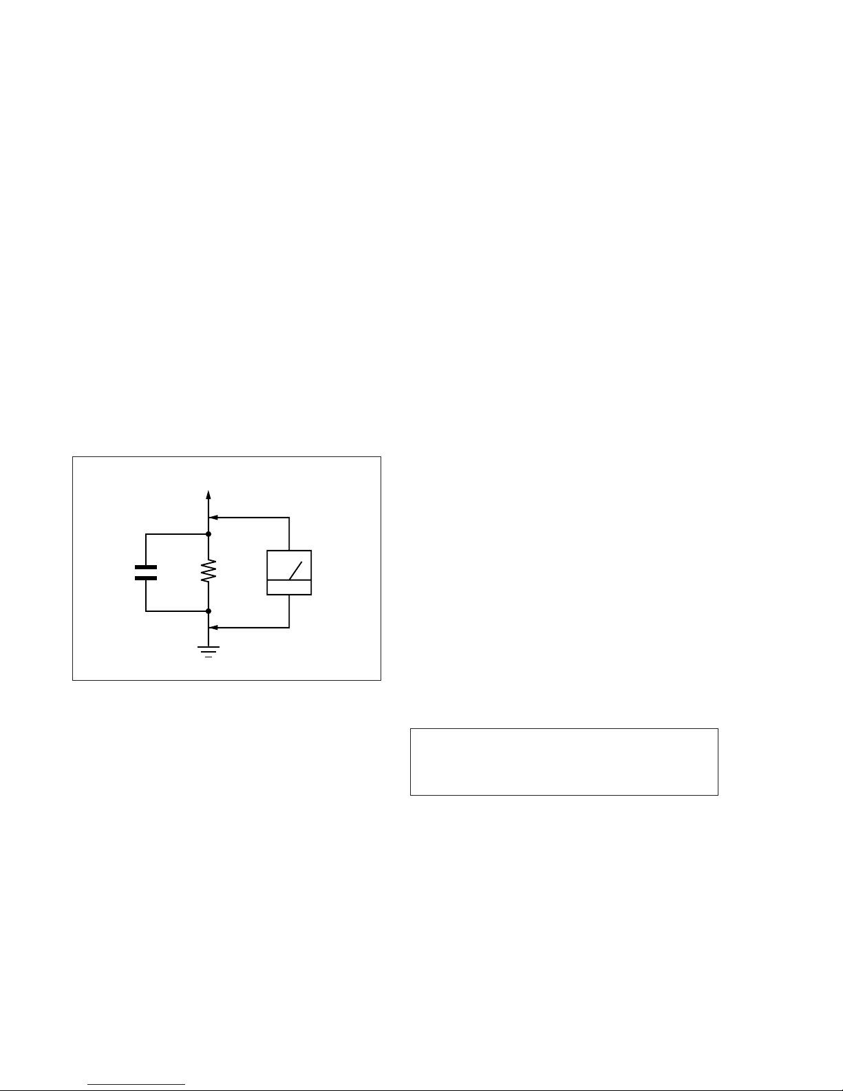
LEAKAGE TEST
The AC leakage from any exposed metal part to earth ground
and from all exposed metal parts to any exposed metal part having
a return to chassis, must not exceed 0.5 mA (500 microamperes).
Leakage current can be measured by any one of three methods.
1. A commercial leakage tester, such as the Simpson 229 or RCA
WT -540A. Follow the manufacturers' instructions to use these
instruments.
2. A battery-operated A C milliammeter. The Data Precision 245
digital multimeter is suitable for this job.
3. Measuring the voltage drop across a resistor by means of a
VOM or battery-operated AC voltmeter. The “limit” indica-
tion is 0.75V, so analog meters must have an accurate low-
voltage scale. The Simpson 250 and Sanwa SH-63T rd are ex-
amples of a passive VOM that is suitable. Nearly all battery
operated digital multimeters that have a 2V A C range are suit-
able. (See Fig. A)
Fig. A Using AC voltmeter to check AC leakage
1.5 k
Ω
0.15 µF
AC
Voltmeter
(0.75 V)
To Exposed Metal
Parts on Set
Earth Ground
WARNING!!
WHEN SERVICING, DO NO T APPR O A CH THE LASER
EXIT WITH THE EYE TOO CLOSELY. IN CASE IT IS
NECESSARY TO CONFIRM LASER BEAM EMISSION,
BE SURE TO OBSERVE FROM A DISTANCE OF
MORE THAN 25 cm FROM THE SURFACE OF THE
OBJECTIVE LENS ON THE OPTICAL PICK-UP BLOCK.
CAUTION:
The use of optical instrument with this product will increase eye
hazard.
ATTENTION AU COMPOSANT AYANT RAPPORT
À LA SÉCURITÉ!
LES COMPOSANTS IDENTIFIÉS P AR UNE MARQUE !
SUR LES DIAGRAMMES SCHÉMA TIQ UES ET LA LISTE
DES PIÈCES SONT CRITIQUES POUR LA SÉCURITÉ
DE FONCTIONNEMENT. NE REMPLACER CES COMPOSANTS QUE PAR DES PIÈCES SONY DONT LES
NUMÉROS SONT DONNÉS DANS CE MANUEL OU
DANS LES SUPPLÉMENTS PUBLIÉS PAR SONY.
1. Check the area of your repair for unsoldered or poorly-soldered connections. Check the entire board surface for solder
splashes and bridges.
2. Check the interboard wiring to ensure that no wires are
“pinched” or contact high-wattage resistors.
3. Look for unauthorized replacement parts, particularly transistors, that were installed during a previous repair. Point them
out to the customer and recommend their replacement.
4. Look for parts which, though functioning, show obvious signs
of deterioration. Point them out to the customer and recommend their replacement.
5. Check the B+ voltage to see it is at the values specified.
6. Check the B+ voltage to see it is at the values specified.
7. Check the antenna terminals, metal trim, “metallized” knobs,
screws, and all other exposed metal parts for AC leakage.
Check leakage as described below.
SAFETY CHECK-OUT
After correcting the original service problem, perform the following
safety checks before releasing the set to the customer:
SAFETY-RELATED COMPONENT WARNING!!
COMPONENTS IDENTIFIED BY MARK ! OR DOTTED
LINE WITH MARK ! ON THE SCHEMATIC DIAGRAMS
AND IN THE PARTS LIST ARE CRITICAL TO SAFE
OPERATION. REPLACE THESE COMPONENTS WITH
SONY PARTS WHOSE PART NUMBERS APPEAR AS
SHOWN IN THIS MANUAL OR IN SUPPLEMENTS PUBLISHED BY SONY.
CAUTION
Use of controls or adjustments or performance of procedures
other than those specified herein may result in hazardous radiation exposure.

– 3 –
TABLE OF CONTENTS
Section Title Page Section Title Page
Service Note ............................................................................ 4
1. GENERAL
This Player Can Play the Following Discs .................... 1-1
Getting Started .............................................................. 1-1
Basic Operations ........................................................... 1-2
Playing Discs in Various Modes .................................... 1-4
Setting and Adjustments ............................................... 1-9
Dolby Digital Surround .................................................. 1-10
Additional Information ................................................... 1-11
2. DISASSEMBLY
2-1. CASE REMOVAL ......................................................... 2-1
2-2. FRONT PANEL SECTION REMOVAL....................... 2-1
2-3. MB-83 BOARD REMOVAL .......................................... 2-1
2-4. REAR PANEL REMOVAL ........................................... 2-1
2-5. TABLE ASS’Y REMOVAL............................................ 2-2
2-6. ROTARY MOTOR ASS’Y (M951) REMOVAL ........... 2-2
2-7. CHASSIS ASS’Y REMOVAL ....................................... 2-2
2-8. LOADING MOTOR ASS’Y (M991) REMOVAL ......... 2-2
2-9. BU HOLDER ASS’Y REMOVAL ................................ 2-3
2-10. TK-48 BOARD REMOVAL .......................................... 2-3
2-11. SKEW MOTOR ASS’Y (M902) REMOVAL............... 2-3
2-12. SLED MOTOR ASS’Y (M501) REMOVAL ................ 2-3
2-13. SPINDLE MOTOR ASS’Y (M901) REMOVAL.......... 2-4
2-14. OPTICAL PICK-UP REMOVAL ................................... 2-4
2-15. INTERNAL VIEWS ....................................................... 2-4
2-16. CIRCUIT BOARDS LOCATION .................................. 2-5
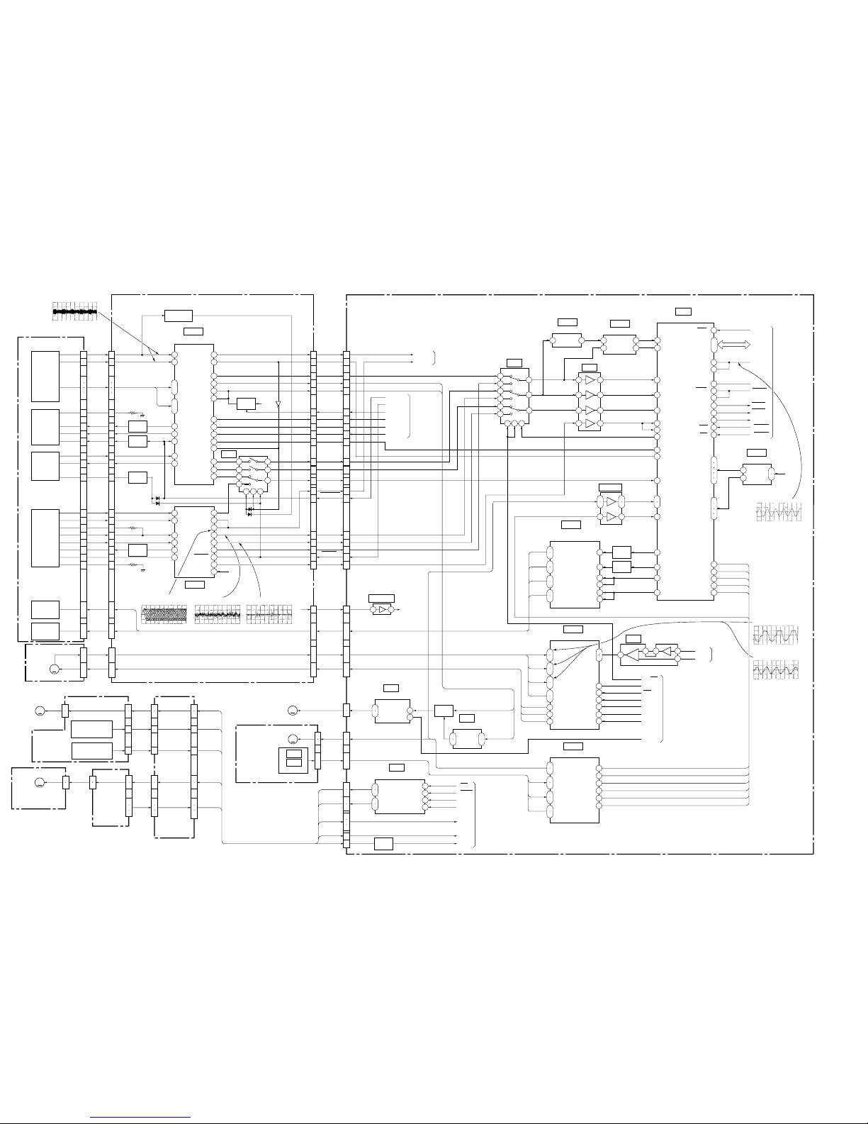
3. BLOCK DIAGRAMS
3-1. Overall Block Diagram .................................................. 3-1
3-2. RF/Servo Block Diagram .............................................. 3-3
3-3. Signal Precess Block Diagram ..................................... 3-5
3-4. Video Block Diagram..................................................... 3-7
3-5. System Control Block Diagram ..................................... 3-9
3-6. Audio Block Diagram..................................................... 3-11
3-7. Mode Control Block Diagram ........................................ 3-13
3-8. Power Block Diagram.................................................... 3-15
4. PRINTED WIRING BOARDS AND SCHEMATIC
DIAGRAMS
4-1. Frame Schematic Diagram............................................ 4-1
4-2. Printed Wiring Boards and Schematic Diagrams ......... 4-5
TK-48 Printed Wiring Board .......................................... 4-5
TK-48 (RF, Servo 1) Schematic Diagram ..................... 4-7
TK-48 (RF, Servo 2) Schematic Diagram ..................... 4-9
MB-83 Printed Wiring Board ......................................... 4-11
MB-83 (AC-3 Decoder) Schematic Diagram ................ 4-15
MB-83 (M Gate Array) Schematic Diagram.................. 4-17
MB-83 (AV Decoder) Schematic Diagram.................... 4-19
MB-83 (Clock Generator) Schematic Diagram............. 4-21
MB-83 (Video Encoder) Schematic Diagram................ 4-23
FG-44 Printed Wiring Board.......................................... 4-26
MB-83 (Drive 1) Schematic Diagram ............................ 4-27
MB-83 (Drive 2), FG-44 Schematic Diagram .............. 4-29
MB-83 (DSP 1) Schematic Diagram ............................. 4-31
MB-83 (DSP 2) Schematic Diagram ............................. 4-33
MB-83 (Roulette), CK-78, LM-55, SE-70
Schematic Diagram ....................................................... 4-35
CK-78, LM-55, SE-70 Printed Wiring Boards ............... 4-37
MB-83 (Bias) Schematic Diagram ................................ 4-39
MB-83 (IF µ-com) Schematic Diagram ......................... 4-41
MB-83 (L Gate Array) Schematic Diagram ................... 4-43
MB-83 (ARP, Decrypt) Schematic Diagram .................. 4-45
MB-83 (System µ-com) Schematic Diagram ................ 4-47
MB-83 (S Gate Array) Schematic Diagram .................. 4-49
AU-198 Printed Wiring Board ....................................... 4-51
AU-198 (Audio 1) Schematic Diagram ......................... 4-55
AU-198 (Audio 2) Schematic Diagram ......................... 4-57
AU-198 (Audio 3) Schematic Diagram ......................... 4-59
AU-198 (Video Buffer) Schematic Diagram .................. 4-61
FL-89, LE-20 Printed Wiring Boards............................. 4-63
FL-89, LE-20 Schematic Diagrams............................... 4-65
FR-134, HP-97 Printed Wiring Boards ......................... 4-67
FR-134, HP-97 Schematic Diagrams ........................... 4-69
HS-934SU Printed Wiring Board .................................. 4-71
HS-934SU Schematic Diagram .................................... 4-73
5. IC PIN FUNCTION DESCRIPTION
5-1. Interface Control Pin Function (MB-83 Board IC604) .. 5-1
5-2 System Control Pin Function (MB-83 Board IC805) .... 5-2
6. TEST MODE
6-1. Starting up Test Mode ................................................... 6-1
6-2. Selection of Check Item ................................................ 6-1
6-2-1. Selected Item Check................................................ 6-1
6-2-2. All Items Check ........................................................ 6-1
6-3. Error Display.................................................................. 6-2
6-4. General Description of Checking Method..................... 6 -2
6-5. Drive Auto Adjustment................................................... 6-10
6-6. Drive Manual Operation ................................................ 6-14
6-6-1. Drive Manual Operation menu screen..................... 6-14
6-6-2. Disc Type .................................................................. 6-14
6-6-3. Manual Control 1...................................................... 6-14
6-6-4. Manual Control 2...................................................... 6-15
6-6-5. Manual Control 3...................................................... 6-15
6-6-6. Manual Adjust 1........................................................ 6-15
6-6-7. Manual Adjust 2........................................................ 6-16
6-6-8. Auto Adjust ............................................................... 6-16
6-6-9. Check ....................................................................... 6-16
6-6-10. EEPROM Data screen Display ................................ 6-17
6-7. Other Operation............................................................. 6-17
6-8. Emergency History ........................................................ 6-18
6-9. Error Code ..................................................................... 6-20
7. ELECTRICAL ADJUSTMENT
7-1. Power Supply Check ..................................................... 7-1
1. HS-934SU Board........................................................... 7-1
7-2. Adjustment of System Control ...................................... 7-2
1. System Clock 27 MHz Adjustment ................................ 7-2
7-3. Adjustment of Video System
1. Video Level Adjustment ................................................ 7-2
2. S-Terminal Output Check .............................................. 7-2
3. Checking Composite Video Output B-Y........................ 7-2
4. Checking Composite Video Output R-Y ....................... 7-3
5. Checking Composite Video Output Y ............................ 7-3
6. Checking S Video Output S-C....................................... 7-3
7. Checking S Video Output DC Level .............................. 7-3
7-4. Adjustment Related Parts Arrangement ....................... 7-4
8. REPAIR PARTS LIST
8-1. Exploded Views ............................................................. 8-1
8-1-1. Main Assembly ......................................................... 8-1
8-1-2. Front Panel Assembly .............................................. 8-2
8-1-3. Table Assembly ........................................................ 8-3
8-1-4. Chassis Assembly .................................................... 8-4
8-1-5. DVD Mechanism Chassis Assembly........................ 8-5
8-2. Electrical Parts List........................................................ 8-6
– 4 –
SERVICE NOTE
1. DISASSEMBLY
• This set can be disassembled in the order shown below.
Set
Case
(Page 2-1)
MB-83 board
(Page 2-1)
Table ass’y
(Page 2-2)
Chassis ass’y
(Page 2-2)
BU holder
ass’y
(Page 2-3)
Rotary motor
ass’y
(Page 2-2)
Loading motor
ass’y
(Page 2-2)
Skew motor
ass’y
(Page 2-3)
Sled motor
ass’y
(Page 2-3)
Spindle motor
ass’y
(Page 2-4)
TK-48 board
(Page 2-3)
Spindle base
(Page 2-3)
Optical pick-up
(Page 2-4)
Front panel
section
(Page 2-1)
Rear panel
(Page 2-1)
– 5 –
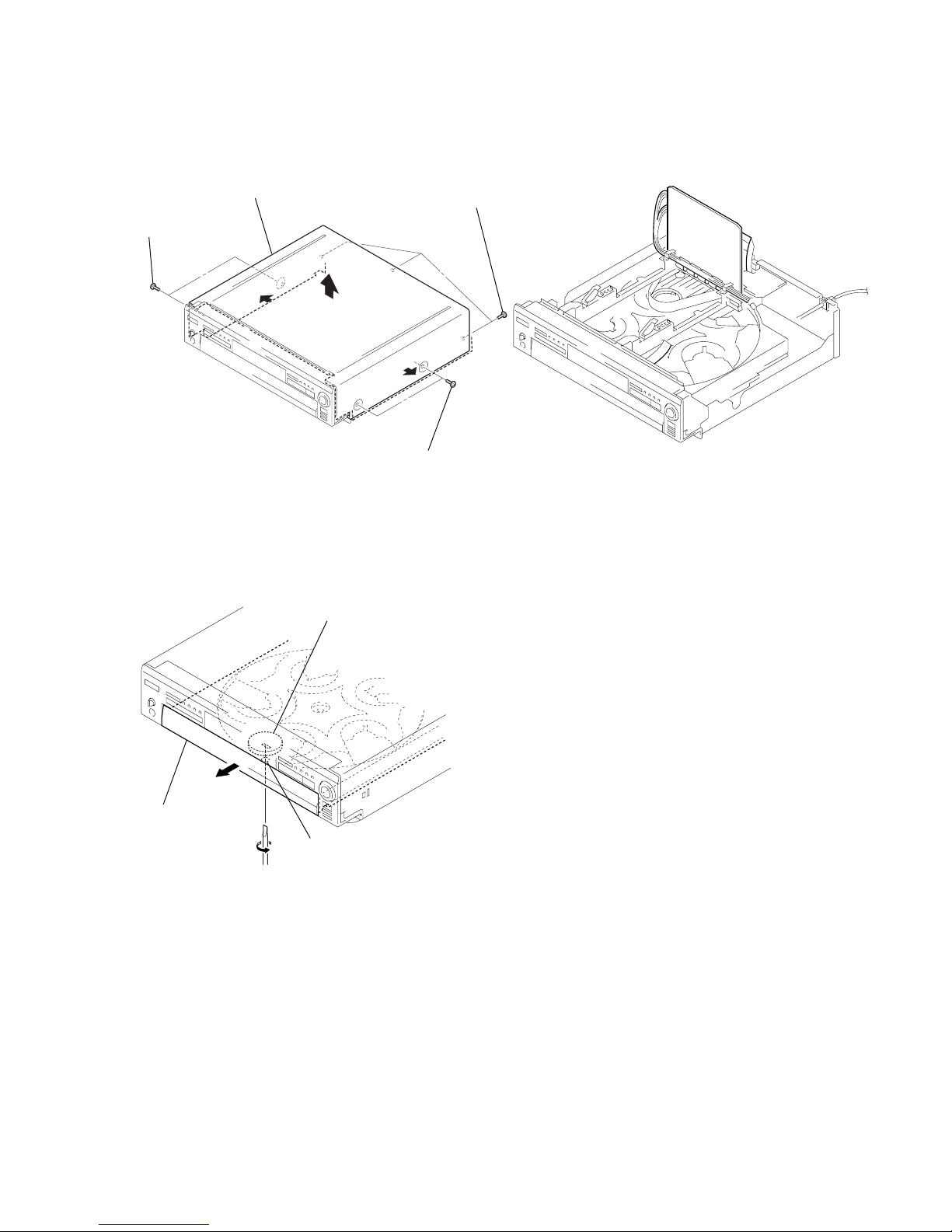
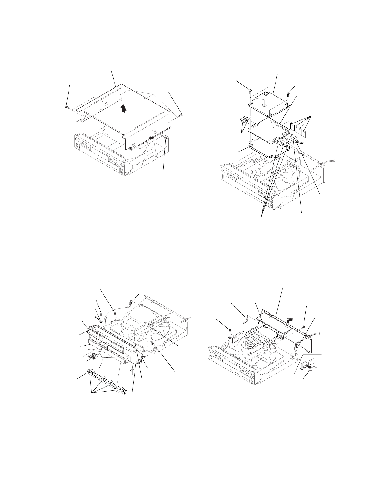
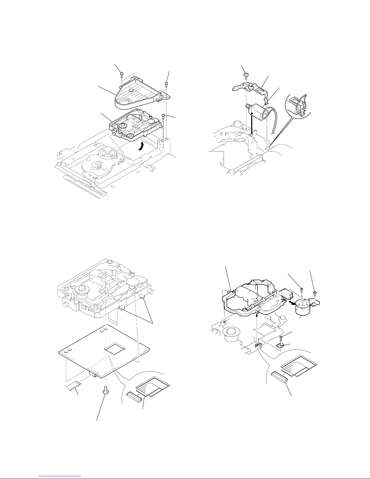
2. NOTE ON REMOVE THE CASE
1) Remove seven tapping screws. (See Fig. 1)
2) Open the side of case. (See Fig. 1)
3) Remove the case as lift straight. (See Fig. 1)
Fig. 1
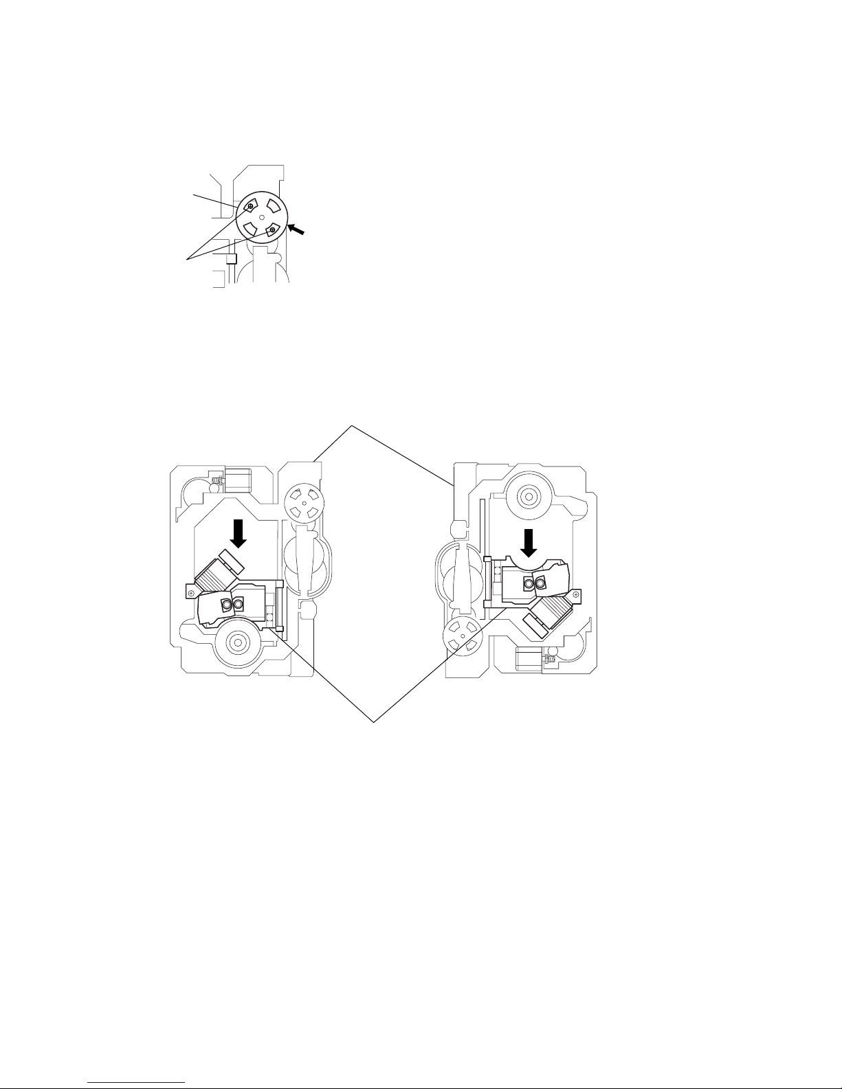
3. DISK REMOVAL PROCEDURE
(at POWER OFF)
1) Insert a flat-blade screwdriver into a hole at the bottom, and
rotate the cam gear in direction A. (See Fig. 2)
Fig. 2
4. HOW TO SERVICE MB-83 BOARD
1) Remove the case from the set. (Refer to 2-1)
2) Remove the MB-83 board. (Refer to 2-3)
3) Set the MB-83 board as shown in Fig. 3.
Note: Do not disconnect wiring.
Fig. 3
Case
Two tapping screws
Three tapping screws
Two tapping screws
Table
Hole
Cam gear
A
– 6 –
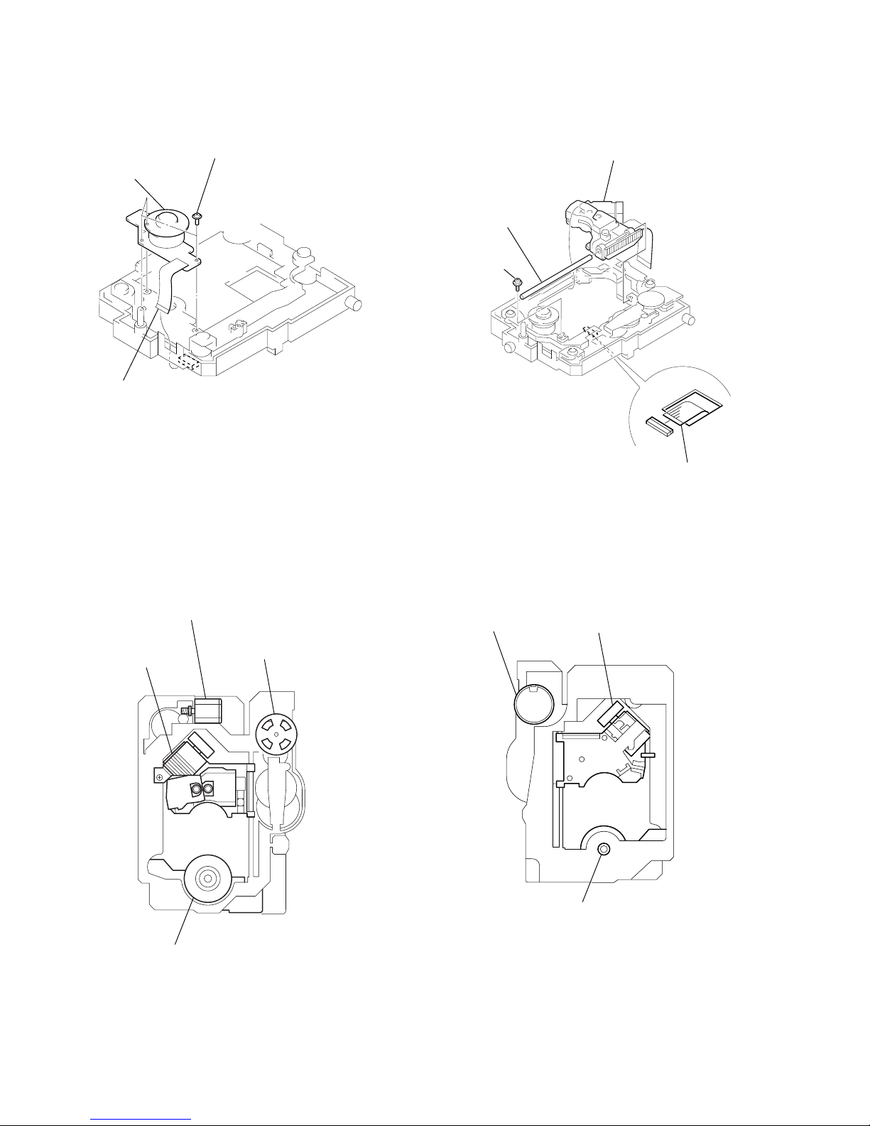
5. NOTE ON MOUNTING SLED MOTOR
1) Push the sled motor ass’y 1 toward direction A. (See Fig. 4)
2) Tighten two screws 2 (M1.7 × 2.5).
Fig. 4
3) Raising the MD block ass’y 3 90 º with the side down.
confirm that the optical pick-up 4 falls by self weight.
(See Fig. 5)
4) Further, with the front side of MD block ass’y 3 up, confirm
that the optical pick-up falls by self weight.
Fig. 5
A
1 Sled motor ass’y
2 Two screws
(M1.7 × 2.5)
Upper
Upper
Front side
Front side
Lower
Lower
3 MD block ass’y
4 Optical pick-up
– 7 –
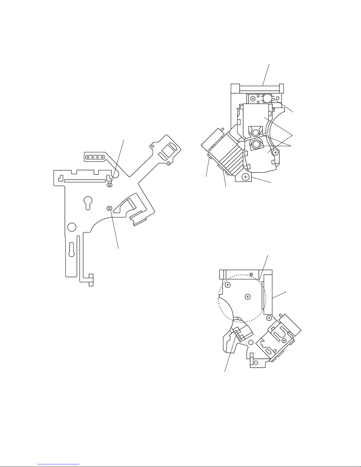
6. REPLACING OPTICAL PICK-UP
6-1. Handling
1) A red laser diode for DVD requires more attention to static
electricity than general infrared laser diodes for CD.
Because its durability to static electricity is far weaker than
that of infrared laser diodes, always use an earth band when
handling the optical pick-up block as service parts.
2) As for the flexible board KHS-180A (RP) packed as service
parts, the short lands have been soldered to protect from static
electricity. Accordingly, remove solders when replacing optical pick-up. (See Fig. 6)
Fig. 6 Flexible board
3) In handling the KHS-180A (RP), do not touch inhibited parts
shown in Fig. 7, but grip the slide base bearing and U-shaped
guide.
Fig. 7 KHS-180A (RP)
Touch inhibited par ts
• Objective lens
• Skew sensor
• Laser holder
• Laser coupler
• Flexible board
• OEIC
• Lens actuator covers
DVD short land
CD short land
Slide base bearing
Skew sensor
Lens actuator
covers
Objective lenses
U-shaped guide
OEIC
Laser holder
Flexible board
Connector
Laser coupler
– 8 –
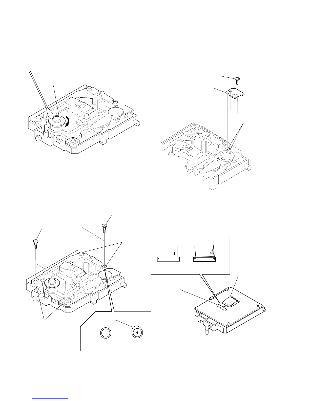
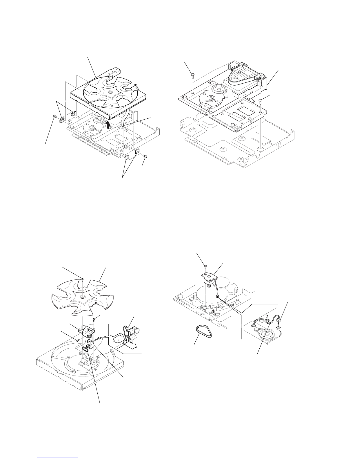
7. NOTE ON ASSEMBLING MECHANICAL DECK
Fig. 11
7-1. Cleaning Spindle Motor Turntable
1) Remove the BU holder ass’y. (Refer to 2-9)
2) Clean the spindle motor turntable if disc antiskid rubber (black)
is dirty. (See Fig.8)
7-2. Deformation of Insulator
1) Assemble the spindle base into the BU holder.
2) Lock with 4 shoulder screws. (See Fig.9)
3) Check if 4 insulators deformed. (See Fig.9)
7-3. Note on Mounting FG-44 Board
1) Align two bosses. (See Fig.10)
2) Fix the board securely with screws (PTPWH2 × 5). (The sen-
sor will not function normally if the board floats up.)
7-4. Note on connecting OPT Harness
1) The optical pick-up could be destroyed unless the OPT harness is connected normally to the connector. (See Fig.11)
Spindle motor
Turn table
Fig. 8
Fig. 9
Two step screws
Two step screws
Two insulators
Two insulators
Insulator
Good
NG
Screw
(PTPWH2 × 5)
FG-44 board
Two bosses
Good
NG
OPT harness
Connector
Fig. 10
– 9 –
8. NOTE ON MOUNTING GEARS
1) Mount the gear (U/D). (See FIg.12.)
2) Rotate the gear (U/D) in the direction of the arrow.
(down position) (See Fig.12.)
3) Align triangle marks of the rotary encoder. (See Fig.13.)
4) Escape the set lever. (See Fig.13.)
5) Connect the boss of the gear (main) with the groove of the
rotary encoder and mount the gear (main). (See Fig.13.)
6) Mount the lock lever (See Fig.14.)
7) Mount the spring (lock lever). (See Fig.14.)
8) Rotate the gear (main) in the direction of the arrow A by 90°
turn. (Gear (U/D) is up position.) (See Fig.15.)
9) Mount the Gear (rev). (See Fig.15.)
10) Fix three stopper washers on the groove of shafts.
(See Fig.15.)
Gear (U/D)
Fig. 12
Fig. 14
Fig. 13
Fig. 15
Spring
(lock lever)
Spring
(lock lever)
Lock lever
Lock lever
Gear
(main)
Gear (main)
Set lever
Boss
Groove
Rotary encoder
Align triangle marks.
BU
Shaft
Stopper washer
Gear (rev)
Gear (main)
Gear (U/D)
Two stopper
washers
Groove
**
*
A
1-1
SECTION 1
GENERAL
This section is extracted from
US model instruction manual.
DVP-C600D
1-2
1-3
1-4

1-5
1-6
1-7

1-8
1-9
1-10
1-11

1-12
1-13
1-13 E
2-1
Note: Follow the disassembly procedure in the numerical order given.
2-1. CASE REMOVAL 2-3. MB-83 BOARD REMOVAL
2-2. FRONT PANEL SECTION REMOVAL
2-4. REAR PANEL REMOVAL
SECTION 2
DISASSEMBLY
DVP-C600D
4 Case
3 Two tapping screws
1 Two tapping screws
2 Three tapping
screws
2 Connector
(CN205)
1 Flat wire
(CN601)
3 Rotate the cam gear
in the direction of
the arrow A.
0 Lug
!¢ Claw
!∞ Front panel section
!™ Claw
!£ Two Claws
!¡ Two screws (B3)
9 Screw (B3)
5 Tray cover
ass’y
8 Screw (B3)
4 Draw out
the table.
A
6 Four claws
7 Tray guard
9 Four flat wires
(CN101, 302,
452, 252)
2 Three flat wires
(CN301, 601, 701)
3 Flat wire
(CN251)
6 Two screws (B3)
5 Three screws
(B3)
4 Connector
(CN361)
1 Two connectors
(CN001, 002)
0 Cover (lower)
7 Cover (upper)
8 MB-83 board
1 Connector
(CN101)
2 Connector
(CN205)
6 Claw
7 Rear panel
5 Claw
3 Two screws
(B3)
4 Tapping screw
2-2
2-5. TABLE ASS’Y REMOVAL 2-7. CHASSIS ASS’Y REMOVAL
2-6. ROTARY MOTOR ASS’Y (M951)
REMOVAL
2-8. LOADING MOTOR ASS’Y (M991)
REMOVAL
6 Flat wire
(CN602)
1 Two screws
(B3)
2 Two brackets
(guide B1)
4 Two brackets
(guide B1)
3 Two screws
(B3)
5 Table ass’y
4 Two screws
(B3)
7 Two screws
(B2.6 × 3)
1 Tapping screw
(M3 × 12)
5 Bracket (RM) ass’y
6 Belt (RM)
2 Table (rotary)
3 Connector
(CN701)
8 Rotary motor ass’y
1 Four screws
(B3)
2 Four screws
(B3)
3 Chassis ass’y
4 Screw (B3)
5 Loading motor ass’y
1 Belt (timing)
3 Harness
2 Connector
2-3
2-9. BU HOLDER ASS’Y REMOVAL 2-11. SKEW MOT OR ASS’Y (M902) REMOVAL
2-10. TK-48 BOARD REMOVAL
2-12. SLED MOTOR ASS’Y (M501) REMOVAL
1 Two screws
(B3)
2 Two screws
(B3)
4 Screw
(B3)
3 Bracket (CP)
5 BU holder ass’y
3 Two screws
(B3)
4 Two claws
2 OP-15 flexible board
(CN001)
1 Flat wire
(CN002)
TK-48 board
2 Claw
3 Skewgear retainer
4 Skewgear motor ass’y
(M902)
1 Screw
(PTTWH2 × 5)
3 Skew shaft stopper
7 Sled motor ass’y
(M501)
5 Screw
(PTTWH2 × 5)
4 Spindle base
1 OP-15 flexible board
(CN001)
2 Screw
(P2 × 8)
6 Two screws
(P1.7 × 2.5)
2-4
2-15. INTERNAL VIEWS
2-13. SPINDLE MOTOR ASS’Y (M901)
REMOVAL
2-14. OPTICAL PICK-UP REMOVAL
3 Spindle motor ass’y
(M901)
2 Three screws
(PTTWH2 × 5)
1 Flat wire
(CN002)
4 Optical pick-up
3 Main shaft
2 Screw
(PTTWH2 × 5)
1 OP-15 flexible board
(CN001)
Skew motor ass’y (M902)
X-3947-138-1
Sled motor ass’y (M501)
X-3947-137-1
Optical pick-up
(KHS-180A/J1N)
8-820-005-02
DC motor (spindle) (M901)
1-763-131-11
Sled motor ass’y (M501)
X-3947-137-1
Optical pick-up
(KHS-180A/J1N)
8-820-005-02
DC motor (spindle)
1-763-131-11
2-5
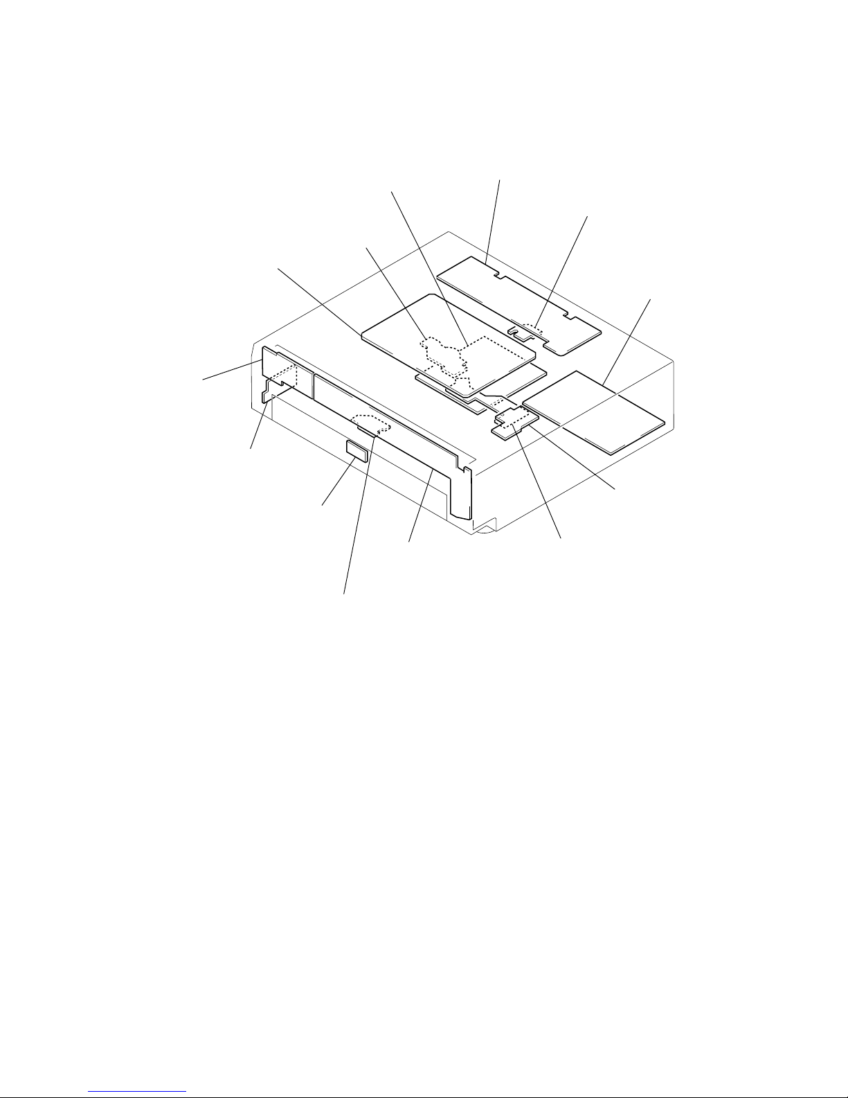
2-16. CIRCUIT BOARDS LOCATION
AU-198
(AUDIO)
FG-44
(SLED)
POWER BLOCK
(HS-934SU)
(POWER SUPPLY)
CK-78
(CONNECTION)
SE-70
(SENSOR)
LM-55
(LOADING MOTOR)
LE-20
(LED)
HP-97
(HEAD PHONE)
FR-134
(FUNCTION
SWITCH)
MB-83
(SIGNAL PROCESS)
DC MOTOR
(SPINDLE)
TK-48
(RF/SERVO)
FL-89
FL DRIVER/
FUNCTION SWITCH
(
)
2-5 E
DVP-C600D
3-1 3-2
SECTION 3
BLOCK DIAGRAMS
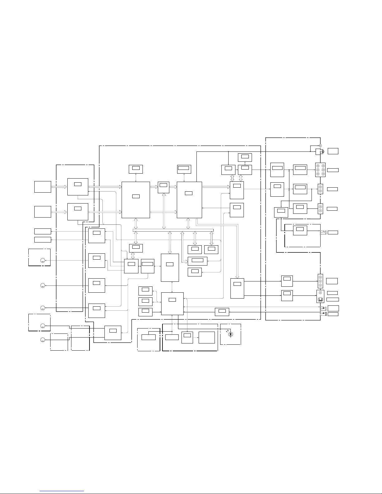
3-1. OVERALL BLOCK DIAGRAM
SE-70 BOARD
(SEE PAGE 4-36)
CK-78 BOARD
(SEE PAGE 4-36)
FR-134 BOARD
(SEE PAGE 4-69)
FL-89 BOARD
(SEE PAGE 4-65)
LE-20 BOARD
(SEE PAGE 4-65)
LM-55 BOARD
(SEE PAGE 4-36)
FG-44 BOARD
(SEE PAGE 4-27)
TK-48 BOARD
(SEE PAGE 4-7~4-10)
MB-83 BOARD
(SEE PAGE 4-15~4-50)
IC006
DVD RF AMP,
SERVO
IC005
CD RF AMP,
SERVO
IC363
FOCUS/TRACKING
COIL DRIVE
IC302
SLED MOTOR
DRIVE
IC303
SPINDLE MOTOR
DRIVE
IC361
TILT MOTOR
DRIVE
IC701
ROULETE
SWITCH
SWITCH
IC604
IC606
IF µ-COM
IC101
FL DRIVER
ND101
FLUORESCENT
INDICATOR TUBE
IC608
256K SRAM
IC605
RESET
IC603
ROM
IC506
SERVO DSP
IC804 (1/2)
LGATE
ARRAY
IC807
S GATE ARRAY
IC802
1M SRAM
YC0-7
IC804 (2/2)
L GATE ARRAY
IC801
EEPROM
IC803
8M ROM
IC806
ARP
IC810
4M DRAM
IC203
AV DECODER
IC201, 202
16M SRAM
IC104
AC-3
DECODER
IC105
256K SRAM
SPDIF
IC102
DIR
IC101
M GATE
ARRAY
AV_DATA, AV_BLK, AV_LRCK
IC215
AUDIO 2CH
DAC
IC851
VIDEO
BUFFER
IC351
VIDEO
BUFFER
IC203-205
DAC
IC208-213
5.1OUTPUT
AUDIO 1, 2
AUDIO IN
PHONE
COMPNENT
VIDEO OUT
MEGA
CONTROL
VIDEO 1, 2
S VIDEO 1, 2
S-LINK
DIGITAL
OUT
MIX AMP
BUFFER
IC206, 207
MIX AMP
BUFFER
IC301
BUFFER
IC214
BUFFER
IC001
HP AMP
IC207
OSD
IC252
VIDEO
ENCODER
IC811
DECRYPT
IC851
SYSTEM µ-COM
DVD OPT
DVD RF
CD RF
HA0-21, HD0-15
CD OPT
FOCUS COIL
TRACKING COIL
M
M
M
M
M
M951
ROTARY
MOTOR
M991
LOADING
MOTOR
M903
TILT
MOTOR
M901
SPINDLE
MOTOR
M503
SLED
MOTOR
S-LINK COMP
SD0-7
CD_BCK,
CD_LRCK,
CD_DATA,
SPDIF
DCRSD
0-7
HP-97 BOARD
(SEE PAGE 4-69)
AU-198 BOARD
(SEE PAGE 4-55~4-62)
05
DVP-C600D
3-3 3-4
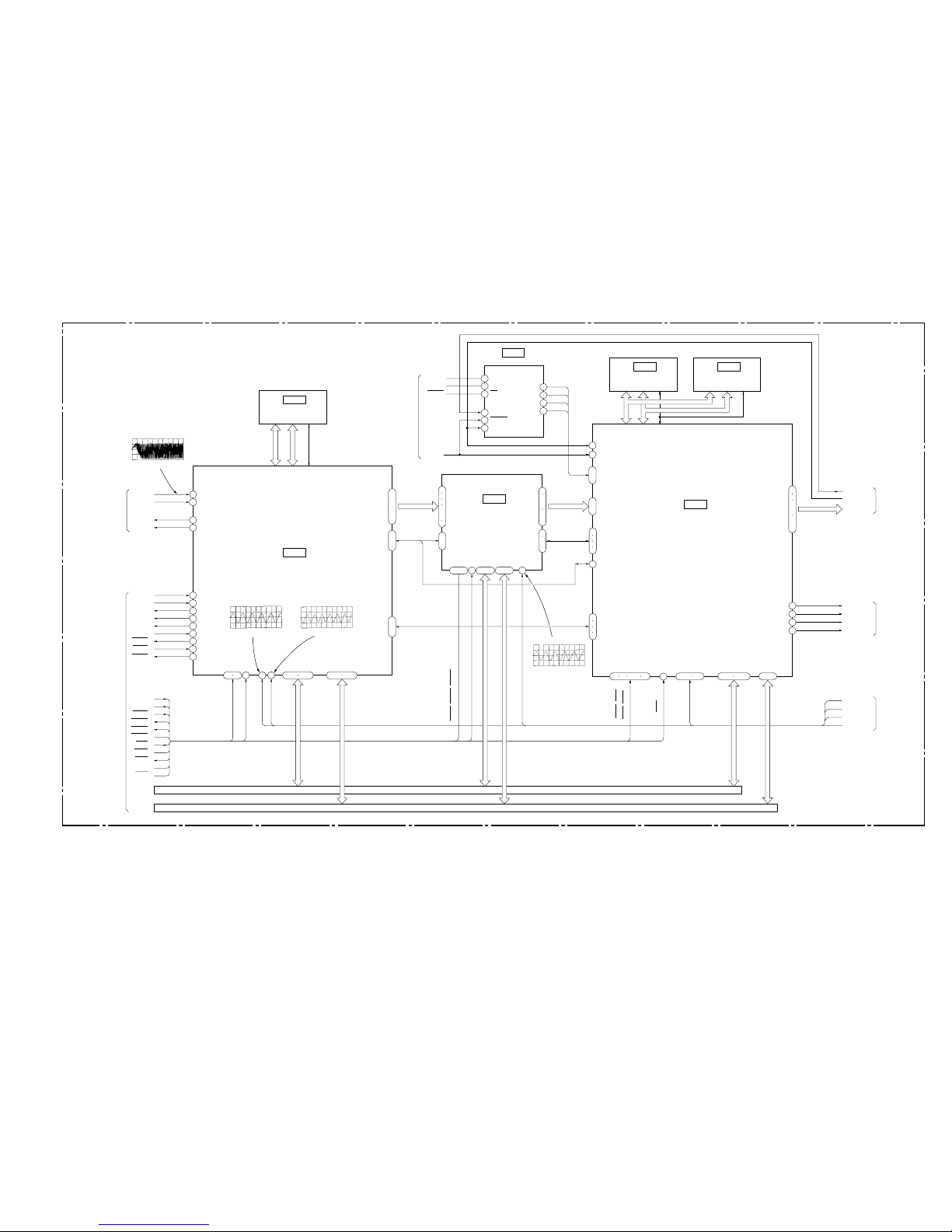
3-2. RF/SERVO BLOCK DIAGRAM
IC363
FOCUS/TRACKING
COIL DRIVER
63
64
57
47
20
9
10
TK-48 BOARD
(SEE PAGE 4-7~4-10)
MB-83 BOARD (1/6)
(SEE PAGE 4-27~4-36)
DVD PD IC
DVD LD
MODULE
SKEW
SENSOR
CD LASER
COUPLER
CD FOCUS
TRACKING
COIL
DVD FOCUS
TRACKING
COIL
Q004
SWITCH
Q008
SWITCH
Q005
SWITCH
Q001
LD ON
Q007
SWITCH
Q009, IC004
RF DET
OPTICAL DEVICE
6
13
14
18
5
41
3
4
2
TI-A
21
42
TI-B
38
16
XLDON
17
PD
18
LD
RFN
RFP
3
338
37
26
23
24
43
44
45
19
33
139
13
4
15
14
30
12
10
28
PD1
4
29
PD2
19
5
27
E
6
20
F
1
23
LD
2
26
PD
19
21
22
13
15
32
25
12
16
25
30
ı
33
34
ı
37
1
ı
8
9
ı
11
9
10
6
13
14
18
5
41
3
4
2
42
38
28
29
19
27
20
23
26
25
30
ı
33
34
ı
37
1
ı
8
9
ı
11
3
ı
10
11
ı
13
26
9
19
3
18
17
4
20
1
22
27
16
21
16
ı
23
25
ı
18
17
ı
15
27
12
ı
5
MIRR
RF02
RF01
TE
FE
RFO
SCLK
SDATA
ADEN
TIOFS
PI
TIE
SIGO
HOLD1
TII
TI–
FDCHG
TE
FE
MIRR
TE_C
VC
9 11
IC006
DVD RF AMP, SERVO
IC011
SWITCH
TTLT/H
10
23
11
14
13
15
12
2
2
19
9
25
10
11
24
8
6
1
12
7
18
5
17
CDRF
14
15
13
16
26
M
M
M
M
M
10
ı
7
A
ı
D
1
ı
4
A2
ı
D2
IC005
CD RF AMP, SERVO
2
4
5
6
5
3
1
2
7
9
11
12
1
2
1
2
PH701
DISK PRESENCE
DETECTION SENSOR
PH702
ROULETTE POSITION
DETECTION SENSOR
3
4
6
1
2
3
4
6
1
2
3
4
6
1
2
11
12
3
4
6
1
2
121
2
ENCODER
ROTARY
(LOADING)
M991
LOADING
MOTOR
SE-70 BOARD
(SEE PAGE 4-36)
LM-55 BOARD
(SEE PAGE 4-36)
CK-78 BOARD
(SEE PAGE 4-36)
FG-44 BOARD
(SEE PAGE 4-27)
1
2
3
ı
8
7
8
1
ı
6
7
9
11
13
5
6
173
5
14
16
4
21
3 1
2
5
22
21
IC701
IC501
M503
SLED MOTOR
M903
TILT MOTOR
IC502
ROULETE
IC361
IC502 (1/2)
TILT MOTOR DEVICE
IC455
COMP
OUT
IN
HALL SENSOR
Q701
BUFFER
Q452
SWITCH
13
12
1
14
4
15
2
109 11
3
5
IC452
89
7
2 1 6 7
3 1
72
TRIN
DFCTA
AIN5
AIN2
AIN0
GIO3
PISW
GIO2
GIO8
PWM2
GIO10
HDO-7
CLKIN
TCK
IRS
VTOP
VBTM
AOUT3
AOUT2
PWM1
GIO0
PWM0
GIO15
GIO9
GIO13
ACK
IA1
IDO-7
27M_DSP
FON
TRREF
AIN6, 7
AIN8
GIO12
AOUT0
AOUT1
IN OUT
IN2 OUT2
IN1 OUT1
IC506
SERVO DSP
IC508
FILTER
IC501
COMP
3 1
6 7
10 8
12 14
21
24
26
11
12
8
73
99
IC503
9
20
6
23
3
1
GIO11
2
88
7
1
49
46
26
IC502 (2/2)
11
12
5107
8
13
14
15
16
17
18
23
22
19
8
9
27
7
10
11
30
31
14
15
32
33
34
1
28
29
75
14
74
41
38
8
12
13
18
25
32
2
5
33
34
29
30
22
23
Q371
MUTE
Q372
MUTE
+
–
IC363
IC303
IC301
SPINDLE MOTOR DRIVE
IC302
SLED MOTOR DRIVE
19
20
3
5
65
79
3
98
4
100
71
70
84
94
56
ı
63
28
37
42
45
50
36
43
44
51
M901
SPINDLE
MOTOR
M951
ROTARY
MOTOR
CN991
LM LM
S1-S3
LM
S1-S3
CN701
CN702
CN603
TM
DSENS
TSENS
TM
DSENS
TSENS
CN602
CN601
TIMT
SLDMT
CN501
CN301
CN361
HA, HB,
SLVH
LM
TM
S1-S3
TSENS
DSENS
CN701
OUT1 +, –
DOUT
FIN1
IN1+
MUTE1
RIN1
FIN2
RIN2
TBLL
TBLR
S1-S3
TSENS
DSENS
OUT2 +, –
SYSTEM CONTROL
(SEE PAGE 3-9)
LDIN
LDOUT
CD FCS,
CD TRK
DVD FCS,
DVD TRK
U IN,
V IN,
W IN,
SPVH
U OUT,
V OUT,
W OUT
U IN,
V IN,
W IN,
SPVH
U OUT,
V OUT,
W OUT
APC_ON
Q009
VC
VC
VC
VC
DVD_RF+
DFCTS
DVD_PI
RFP
CN001
RFN
A-D
VR
DVD LD
PD
VLD
SKEW IN
SKEW OUT
LED
PD1
PD2
AL
CD_E
CD_F
CD_LD
MON
VR
TI-ERR
TIE
SSSD
SCKG3
SDEN
TIOFS
DPD
DVD_FE
MIRR
DVD LDON
CD TE
CD FE
CDRFDC
TEATT
CD LDON
SVC
DVDFCS,
DVDTRK
CDFCS,
CDTRK
TIE
TI_ERR
DVD RF
CD RF
TIE
TI_ERR
DVD LDON
CD LDON
TILT/H
SSSD
SCKG3
SDEN
SYSTEM
CONTROL
(SEE PAGE 3-9)
SIGNAL PROCESS
(SEE PAGE 3-5)
12 14
DO2
CD TRK
CDFCS
DVDFCS
DVDTRK
MUTE1
DO1 MUTE2
DO4
IN2–
DO3
IN1–
IN3–
IN4–
U IN
V IN
W IN
VH
Z1, Z2
U OUT
SPCTRL0
SPCTRL1
NS+
HFG
V OUT
SPGC2
W OUT
SPGC1
SPCTRL0
SPCTRL1
HFG
MDP0
MDS0
SPGC2
SPGC1
S12VOFF
SLDMT
DV–
HA
DVI
HB
DVO
SLVH
TKC
CTRL
A+
SDCNT
SOUT
SLOFS
TKC
HYCNTR
HYDET
SYSTEM CONTROL
(SEE PAGE 3-9, 10)
671 2
5
SIGNAL
PROCESS
(SEE PAGE 3-5)
NST
18
HCK/HLDB
MRST
HR/HRD
HFD/HWR
SDPRST
ERROR
BUSY2
SDSPWR
SDSPRD
OUT2
OUT1
IN
VC
IC507
POWER SUPPLY
SYSTEM CONTROL
(SEE PAGE 3-9, 10)
SDCNT
SOUT
SLOFS
TKC
HYCNTR
HYDET
CN002
CN008
CN302
CN005
CN452
CD/DVD
05
IC006 ^£ – ^¢ (DVD play)
800 mVp-p (V)
IC005 @™ (CD play)
500 mV/DIV 1 µs/DIV
IC005 !£ (CD play)
500 mV/DIV 1 ms/DIV
IC005 !∞ (CD play)
500 mV/DIV 10 ms/DIV
IC506 ^∞
3.6 Vp-p 27 MHz
IC303 !ª, @™, @£ (DVD play)
5.2 Vp-p 160Hz
IC303 !ª, @™, @£ (CD play)
1.84 Vp-p 45Hz
DVP-C600D
3-5 3-6
3-3. SIGNAL PROCESS BLOCK DIAGRAM
IC806
ARP
IC811
DECRYPT
IC207
OSD
IC203
AV DECODER
IC810
4M DRAM
10
RF IN1DVD RF
12
RF IN2CD RF
69
VS
70
HS
DCK
EX_OSD_0-3
CH-DATA0-7
OH SYNC
43
MDS0MDS0
48
MDP0MDP0
110
MUTE
112
MD2
50
DFCT
51
NORF
53
LOCK
55
FWON
80
XINT
81
XCS
83
84 122
XWAT
XRST
XWR, XRD
XRST
27M_DSP
33M
MCKI
SCKI
A0-7
D0-7
MUTE
MD2
DFCT
NORF
LOCK
FWON
XWR
XRD
XRST
IA0-8
ID0-7
05
24
SCLK
SO
25
SIN
SCLKO
26
20
19
18
17
R OUT
G OUT
B OUT
I OUT
11
EVEN
12
13
V SYNC
MA0-9
MD00-15
XMWR, XCAS,
XRAS, XOE
124
70-73 75-7856 57
43-47 26-31 34-41
56-62 64-67
106
ı
109
106
ı
109
96
ı
99
101
ı
106
4
ı
8
56
59
ı
61
88
ı
91
12
ı
19
1
3
74
77
ı
79
80
62
64
ı
66
68
ı
74
DCRCS
DCRINT
DCRWT
AVDRQ
AVCS
AVINT
AVWT
MRST
RF/SERVO
(SEE PAGE 3-3, 4)
SYSTEM CONTROL
(SEE PAGE 3-9, 10)
IA0-7
ID0-7
IA0-8
ID0-7
SD0-7
SD0-7 DCRSD0-7
AREQ, ALALID,
ERROR, TOS
DTI0-7
DTO0-7
SDCK, XSHD,
XSRO, XSAK, SDEF
CD_LRCK, CD_BCK,
CD_DATA, SPDIF
54 51
28
111
105
106
107
SYSTEM CONTROL
(SEE PAGE 3-9, 10)
CGCSO
CS
IC201
16M SDRAM
AVA0-11
AVID
0-15
IC202
16M SDRAM
SDQM, WE, CAS, RAS, CS1, CS2, SDQM, SDCLK
A_0-8
D_0-7
21
24
26
30
98
99
101
102
XRST
384FS
IA0-5
ID0-7
27M_DNR
XWR, XRD,
DCRCS, DCRINT, DCRWT
KESET_B
58 59 63-65 68 94-96 100 34-39 43-45 47-54
57
XWR, XRD,
AVDRQ, AVCS,
AVINT, AVWT
MRST
SPDIF_OUT
BCLK
LRCLK
ASDATA
SPDIF
AV_BCK
AV_LRCK
AV_DATA
YC0-7
FID
V SYNC
73
74
76
ı
78
82
ı
84
PD0-7
AUDIO
(SEE PAGE 3-11)
VIDEO
(SEE PAGE 3-7)
384FS
27M_DNR
27M_DSP
33M
SYSTEM CONTROL
(SEE PAGE 3-10)
MB-83 BOARD (2/6)
(SEE PAGE 4-19, 4-45)
XRST
SHA0-5
SHD0-7
MCK
H SYVC
ARPWT
ARPINT
ARPCS
IC806 0
1.5 Vp-p
IC806 `⁄¤¤
3.4 Vp-p 27 MHz
IC806 `⁄¤›
3.0 Vp-p 33 MHz
IC811 %¡
3.4 Vp-p 27 MHz
 Loading...