

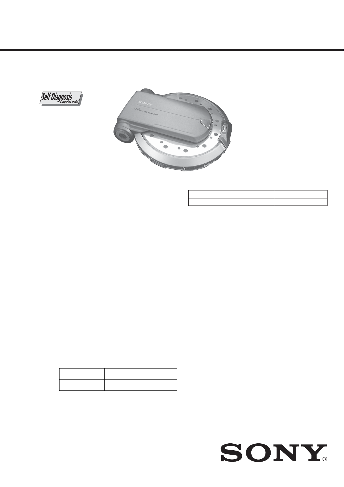
D-VM1
SERVICE MANUAL
Ver 1.2 2002. 04
SPECIFICATIONS
System
Laser Semiconductor laser
Signal format system
(monitor unit)
Signal format system
(AV output adaptor)
Audio characteristics (output signal from AV outpuadt
aptor when “SOUND MODE” is set to “NORMAL”)
Frequency response DVD (PCM 96 kHz): 4 Hz to 44 kHz (±1 dB)*
Signal-to-noise ratio (S/N ratio) 110 dB* (AUDIO OUT jack only)
Harmonic distortion 0.005%
Dynamic range DVD: 103 dB*
Wow and flutter Less than detected value (± 0.001% W PEAK)
Maximum power output (at DC) 25 mW + 25 mW (16 ohms)
*The signals from AUDIO OUT jack are measured. When you play PCM sound tracks with
a 96 kHz sampling frequency, the output signal from the OPTICAL jack is converted to
48 kHz sampling frequency.
General
Power requirements DC 10 V
Battery life
When the cover of the
monitor unit is open
When the cover of the
monitor unit is closed
Power consumption 6 W
Dimensions (approx.) 150.2 × 31.8 × 167.7 mm (6 × 1 5/16 × 6 5/8 inches)
Mass (approx.) 332 g (11.7 oz) (player only), 571 g (1 lb 4 oz)
Operating temperature 5°C to 35°C
Operating humidity 25% to 80%
PAL/NTSC
VIDEO CD:
DVD: Disc’s color system
DVD (PCM 48 kHz): 4 Hz to 22 kHz (±1 dB)*
CD: 4 Hz to 20 kHz (±1 dB)*
CD: 99 dB*
Rechargeable battery (supplied, LIP-30, 7.4 V, 3000 mAh,
Lithium-ion)
Dry batteries (2 for the remote)
(width/height/depth)
(with rechargeable battery)
PAL, NTSC
about 4 hours
about 5 hours
Monitor unit
LCD screen 3.5-inch TFT monitor
AV output adaptor
OPTICAL jack Mini jack, Maximum output level -18 dBm,
AUDIO OUT jack Mini jack, Maximum output level 2 Vrms (50 kilohms),
VIDEO OUT jack Mini jack, Maximum output level 1.0 Vp-p,
S VIDEO OUT jack 4-pin mini DIN,
AC power adaptor
Power requirements 100 to 240 V AC, 50/60 Hz
Supplied accessories
Specifications and design ar e subject to change without no t ice.
US Model
Canadian Model
AEP Model
UK Model
E Model
Chinese Model
Tourist Model
Model Name Using Similar Mechanism NEW
CD Mechanism Type CDM-501
Load impedance Wave length 660 nm
Load impedance Over 10 kilohms
Load impedance 75 ohms, sync negative
Maximum output level:
Luminance signal:1.0 Vp-p, Load impedance 75 ohms,
sync negative
Color signal: 0.3 Vp-p (PAL), 0.286 Vp-p (NTSC), Load
impedance 75 ohms terminated
AC power adaptor (1)
AC power cord (mains lead) (1)
Rechargeable battery LIP-30 (1)
Headphones (1)
Remote commander (remote) (1)
Audio/video cord (miniplug x 2 y pinplug x 3) (1)
Monitor unit (1)
AV output adaptor (1)
Stand (1)
Carrying porch (1)
Strap for the monitor unit (1)
AC plug adaptor (1) (For the tourist models only)
PORTABLE CD/DVD PLAYER
9-873-411-03
2002D1600-1
© 2002.04
Sony Corporation
Personal Audio Company
Published by Sony Engineering Corporation

D-VM1
Ver 1.2 2002.04
TABLE OF CONTENTS
1. SERVICING NOTE·························································· 4
2. GENERAL ·········································································· 5
3. DISASSEMBLY ································································ 7
4. TEST MODE···································································11
5. DIAGRAMS······································································21
5-1. Block Diagram – RF/SERVO Section – ····················· 22
– A/V, SYSCON Section – ··········································23
– AUDIO Section – ····················································· 24
– VIDEO OUT Section – ············································ 25
– POWER Section – ···················································· 26
– TFT Section – ··························································· 27
5-2. Printed Wiring Board
– MAIN Section (Side A) (Over All View) – ··············28
5-3. Printed Wiring Board
5-4. Printed Wiring Board
5-5. Printed Wiring Board
5-6. Printed Wiring Board
5-7. Printed Wiring Board
– MAIN Section (Side B) (Over All View) – ·············· 33
5-8. Printed Wiring Board
5-9. Printed Wiring Board
5-10. Printed Wiring Board
5-11. Printed Wiring Board
5-12. Schematic Diagram – MAIN Section (1/11) – ·········· 38
5-13. Schematic Diagram – MAIN Section (2/11) – ·········· 39
5-14. Schematic Diagram – MAIN Section (3/11) – ·········· 40
5-15. Schematic Diagram – MAIN Section (4/11) – ·········· 41
5-16. Schematic Diagram – MAIN Section (5/11) – ·········· 42
5-17. Schematic Diagram – MAIN Section (6/11) – ·········· 43
5-18. Schematic Diagram – MAIN Section (7/11) – ·········· 44
5-19. Schematic Diagram – MAIN Section (8/11) – ·········· 45
5-20. Schematic Diagram – MAIN Section (9/11) – ·········· 46
5-21. Schematic Diagram – MAIN Section (10/11) – ········ 47
5-22. Schematic Diagram – MAIN Section (11/11) – ········ 48
5-23. Printed Wiring Board – TFT Section (Side A) –········ 49
5-24. Printed Wiring Board – TFT Section (Side B) –········50
5-25. Schematic Diagram – TFT Section (1/3) – ················ 51
5-26. Schematic Diagram – TFT Section (2/3) – ················ 52
5-27. Schematic Diagram – TFT Section (3/3) – ················ 53
5-28. IC Block Diagrams ····················································· 54
5-29. IC Pin Function Descriptions······································59
– MAIN Section (Side A) (1/4) – ·········
– MAIN Section (Side A) (2/4) – ·········
– MAIN Section (Side A) (3/4) – ·········
– MAIN Section (Side A) (4/4) – ·········
– MAIN Section (Side B) (1/4) – ·········
– MAIN Section (Side B) (2/4) – ·········
– MAIN Section (Side B) (3/4) –·········
– MAIN Section (Side B) (4/4) –·········
29
30
31
32
34
35
36
37
6. EXPLODED VIEWS ······················································ 63
7. ELECTRICAL PARTS LIST ······································· 66
This appliance is classified as a CLASS 1 LASER product.
The CLASS 1 LASER PRODUCT MARKING is located on
the rear exterior.
CAUTION
Use of controls or adjustments or performance of procedures
other than those specified herein may result in hazardous
radiation exposure.
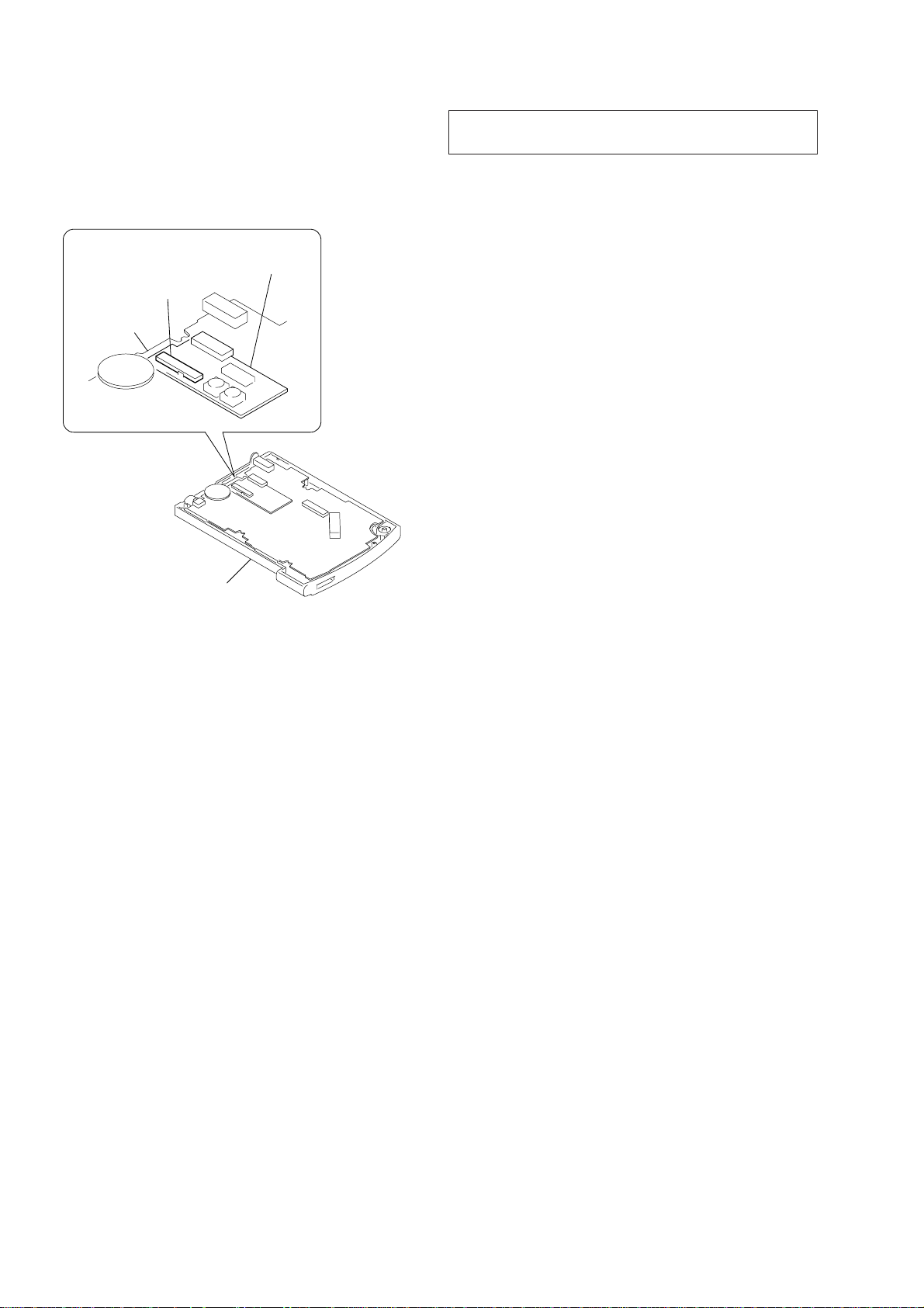
Flexible Circuit Board Repairing
•Keep the temperature of the soldering iron around 270 ˚C during repairing.
• Do not touch the soldering iron on the same conductor of the
circuit board (within 3 times).
• Be careful not to apply force on the conductor when soldering
or unsoldering.
Notes on chip component replacement
•Never reuse a disconnected chip component.
• Notice that the minus side of a tantalum capacitor may be damaged by heat.
Unleaded solder
Boards requiring use of unleaded solder are printed with the leadfree mark (LF) indicating the solder contains no lead.
(Caution: Some printed circuit boards may not come printed with
the lead free mark due to their particular size.)
: LEAD FREE MARK
Unleaded solder has the following characteristics.
• Unleaded solder melts at a temperature about 40°C higher than
ordinary solder.
Ordinary soldering irons can be used but the iron tip has to be
applied to the solder joint for a slightly longer time.
Soldering irons using a temperature regulator should be set to
about 350°C.
Caution: The printed pattern (copper foil) may peel away if the
heated tip is applied for too long, so be careful!
• Strong viscosity
Unleaded solder is more viscous (sticky, less prone to flow) than
ordinary solder so use caution not to let solder bridges occur such
as on IC pins, etc.
• Usable with ordinary solder
It is best to use only unleaded solder but unleaded solder may
also be added to ordinary solder.
SAFETY-RELATED COMPONENT WARNING!!
COMPONENTS IDENTIFIED BY MARK 0 OR DOTTED LINE WITH
MARK 0 ON THE SCHEMATIC DIAGRAMS AND IN THE PARTS
LIST ARE CRITICAL TO SAFE OPERATION. REPLACE THESE
COMPONENTS WITH SONY PARTS WHOSE PART NUMBERS
APPEAR AS SHOWN IN THIS MANUAL OR IN SUPPLEMENTS
PUBLISHED BY SONY.
2
ATTENTION AU COMPOSANT AYANT RAPPORT
À LA SÉCURITÉ!
LES COMPOSANTS IDENTIFÉS P AR UNE MARQUE 0 SUR LES
DIAGRAMMES SCHÉMA TIQUES ET LA LISTE DES PIÈCES SONT
CRITIQUES POUR LA SÉCURITÉ DE FONCTIONNEMENT. NE
REMPLACER CES COMPOSANTS QUE PAR DES PIÈSES SONY
DONT LES NUMÉROS SONT DONNÉS DANS CE MANUEL OU
DANS LES SUPPÉMENTS PUBLIÉS PAR SONY.

Self-diagnosis Function
(When letters/numbers appear in the
display)
When the self-diagnosis function is activ ated
to prevent the player from malfunctioning, a
five-character service number (e.g., C 13 00)
with a combination of a letter and digits
appears on the screen. In this case, check the
following table.
C:13:00
D-VM1
On cleaning
• Fingerprints or dust on a disc may cause
deteriorated image or sound quality. Leave
the disc clean.
• Wipe the disc with a soft cloth from the
center out.
• If the disc is very dirty, first wipe it with a
damp cloth, then wipe it again with a dry
cloth.
• Do not use solvents such as benzine,
thinner, commercially available cleaners, or
anti-static spray intended for vinyl LPs.
First three
characters
of the
service
number
C 13 The disc is dirty.
Cause and/or corrective
action
, Clean the di sc with a sof t cloth
,
The player cannot play the
disc, etc.
The player cannot play the following discs:
xDVD
• DVD-ROM
• DVD-RAM
• DVD Audio discs
• DVD-RWs recorded in video recording
format (VR mode)
xCD
• CD-ROMs (PHOTO CDs included)
• All CD-Rs/RWs other than music format
and VCD format CD-Rs/RWs
• Data part of CD-Extras
• CDs recorded in DTS*
*
If you playback a CD recorded in DTS,
excessive noise may be heard from
headphones output or the AUDIO OUT
jack.
xSuper Audio CD
• The player, however, can play CD layer in
hybrid discs.
Also, the player ca nnot play the following
discs:
• A DVD with a different region code
Region Code
This system is used to protect copyrights. A
region number is allocated on each DVD
player or DVD disc according to the sales
region. Each region code is shown on the
player as well as on the disc packaging. The
player can play the discs that match its region
code. The player can also play discs with the
ALL
mark. Even when the region code is not
shown on the DVD, the region limit may still
be activated.
• A disc that has a non-standard shape (e.g.,
card, heart).
• A disc with paper or stickers on it.
• A disc that has the adhesive of cellophane
tape or a sticker still left on it.
3
D-VM1
SECTION 1
SERVICING NOTE
Note: If you are going to repair the monitor unit.
Do not touch the inverter unit and piezo-electric transformer that
are mounted on the TFT board both in the statuses of power-on and
power-off.
(Touching these components may damage them.)
INVERTER UNIT
piezo-electric transformer
TFT BOARD
NOTES ON HANDLING THE OPTICAL PICK-UP
BLOCK OR BASE UNIT
The laser diode in the optical pick-up block may suffer electrostatic
breakdown because of the potential difference generated by the
charged electrostatic load, etc. on clothing and the human body.
During repair, pay attention to electrostatic breakdown and also use
the procedure in the printed matter which is included in the repair
parts.
The flexible board is easily damaged and should be handled with
care.
NOTES ON LASER DIODE EMISSION CHECK
The laser beam on this model is concentrated so as to be focused on
the disc reflective surface by the objective lens in the optical pickup block. Therefore, when checking the laser diode emission,
observe from more than 30 cm away from the objective lens.
MONITOR UNIT
4
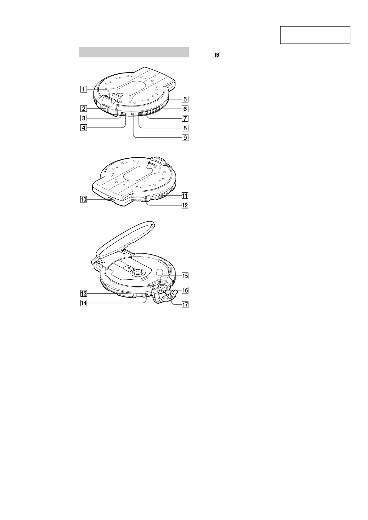
Player
SECTION 2
GENERAL
A OPEN knob
B (remote sensor)
C CHG (charge) indicator
D POWER indicator
E HOLD switch
F VOL (vo lume) +/ – buttons
G ./> (previous/next) buttons
H NX (play/pause) button
I x/OFF (stop/power off) button
J Rechargeable battery terminal
K A/V OUT (audio/video output) jack
L DC IN 10V jack
M MONITOR jack
N i (headphones) jack
O AVLS (Automatic Volume Limiter
P NTSC/PAL switcha
Q Buckle (2 1)
D-VM1
This section is extracted
from instruction manual.
The VOL + button has a tactile dot.
The NX button has a tactile dot.
System) swi t ch
5
D-VM1
Monitor unit
The buttons on the monitor unit work
differently when they are operated with the
SHIFT button.
A SHIFT button
B BRIGHT knob
CDi (headphones) jack
HOLD switch
E ./> (previous/nex t) buttons
When operated with SHIFT:
Slow motion/One fram e pla y ba c k
buttons
F VOL (volume) +/– buttons
The VOL + button has a tactile dot.
When operated with SHIFT:
+: TIME/TEXT button
–: CLEAR button
G NX (play/pause) button
The NX button has a tactile dot.
When operated with SHIFT:
SOUND MODE button
H b/v/V/B/ENTER buttons
When operated with SHIFT:
b: ORETURN button
v: MENU button
V: DISPLAY button
B: TOP MENU button
ENTER: TIMER button
I x/OFF (stop/power off) button
When operated with SHIFT:
Releases Resume Play or returns to PBC
playback.
J POWER indic ator
Remote
A S HUFFLE button
B AUDIO b utton
CDPROGRAM button
ANGLE button
E SUBTITLE button
F REPEAT button
G ./> PREV (previous) /NEXT
buttons
H / SCAN/SLOW butt ons
I H PLAY button
J TOP MENU button
K DISPLAY button
L SOUND MODE button
M Number buttons
N TIME/TEXT button
O CLEAR button
P x STOP/power off button
Q X P AUSE button
R MENU button
S ENTER button
T ORETURN button
U C/X/x/c buttons
6

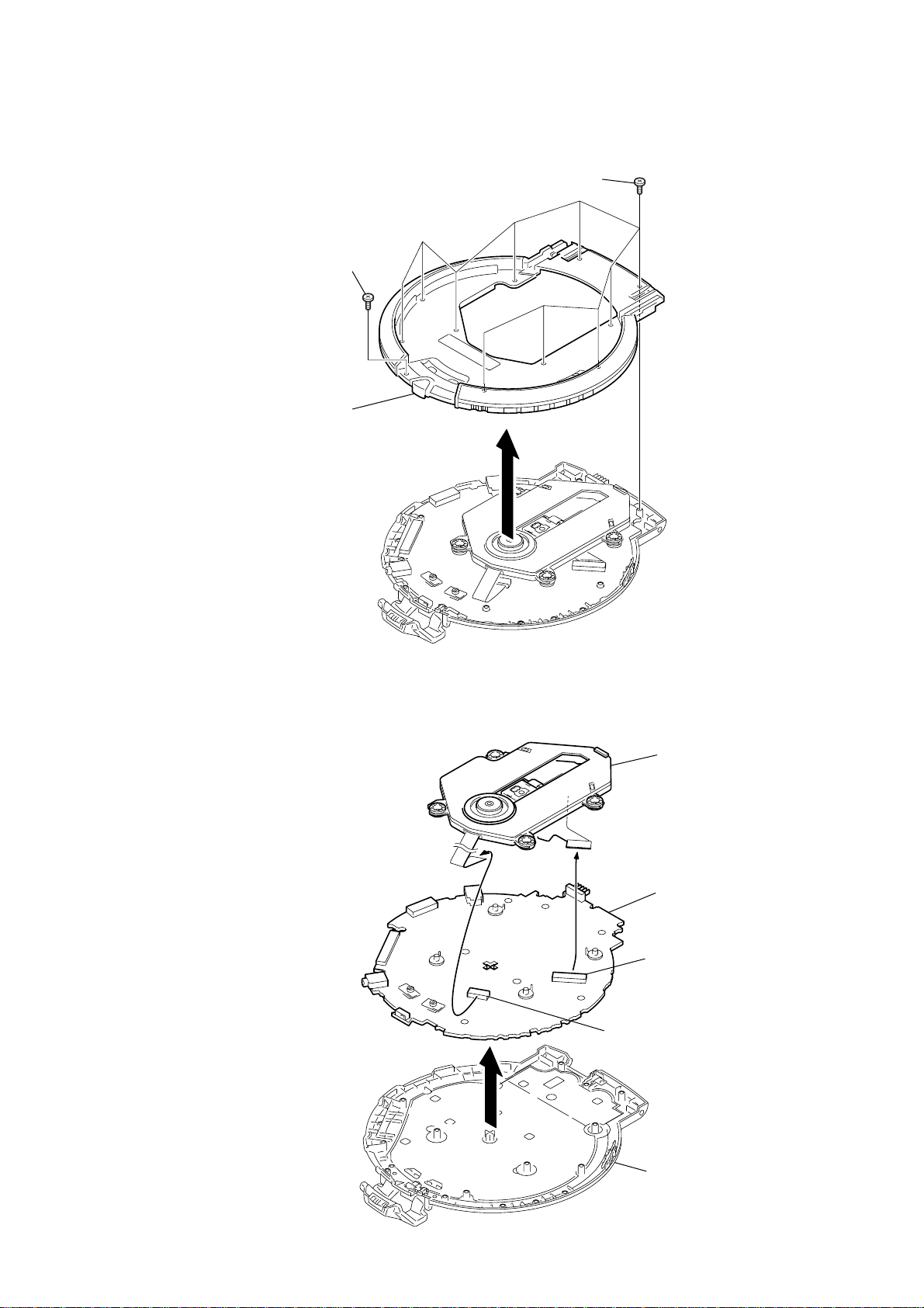
DISASSEMBLY
3
Release the claws in the direction of the arrow
in the order starting from step
A
to E.
6
Cord, connection (Monitor)
5
Connector, 30pin (CN1302)
A
B
C
D
E
Claw
Two claws
Claw
Claw
4
Cabinet
(Rear M)
TFT board, complete
Piezo-electric transformer
Inverter unit
Note: If you are going to repair the monitor unit.
Do not touch the inverter unit and piezo-electric transformer
that are mounted on the TFT board both in the statuses
of power-on and power-off.
(Touching these components may damage them.)
Note : Disassemble the unit in the order as shown below.
D-VM1
SECTION 3
Monitor unit section
Set Lid (disc)
Main section
Cabinet (rear), Connection coard (monitor)
Cabinet (upper)
Note : Follow the disassembly procedure in the numerical order given.
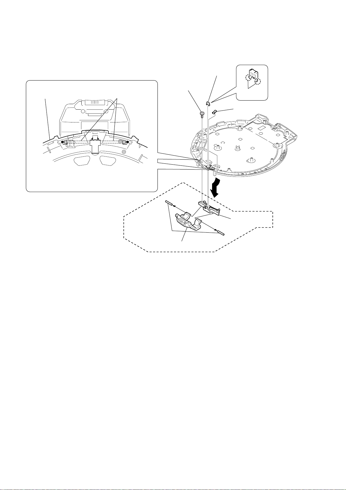
3-1. CABINET (REAR), CONNECTION CORD (MONITOR)
Lid (LCD M)
Inverter unit,
Liquid crystal indicator display (LCD901)
CDM501, Main board
1
Three screws (+BM1.7 × 6)
TFT board,
Buckle
2
7

D-VM1
3-2. INVERTER UNIT, TFT BOARD, LIQUID CRYSTAL INDICATOR DISPLAY (LCD901)
Connector, 3pin
1
(Inverter unit)
5
Connector, 24pin (CN1401)
3
Inverter unit
2
Remove the six soldrings.
7
Spacer (M)
8
Button (Shift M)
4
Two screws (+BM1.7 × 6)
6
TFT board, complete
Knob (Direction key M)
Knob (Play M)
3-3. LID (DISC)
qa
Liquid crystal indicator
display (LCD901)
Knob (Open)
6
Lid (Disc)
3
Screw (M1.4), step
q;
9
Claw
Cabinet (Front M)
5
1
2
4
Screw (M1.4), step
Buckle
8
3-4. CABINET (UPPER)
)
4
Cabinet (Upper)
2
screw, tapping
1
Ten screws (+BM1.7 × 6)
3
D-VM1
3-5. CDM501, MAIN BOARD
3
CDM501
5
Main board, complete
1
Connector, 30pin (CN601
2
4
Connector, 8pin (CN1601)
Cabinet (Lower)
9
D-VM1
3-6. BUCKLE
Cabinet (Lower)
4
Press the two shafts (buckles) that are located in the
recessed areas in the right and left of the cabinet (lower)
in the direction of the arrows respectively.
Shaft (Buckle)
Stopper (Shaft)
2
1
Two screws, tapping
5
Two claws
3
Lever (Battery direction)
6
Shaft (Buckle)
8
Buckle
7
Base, buckle
10

SECTION 4
TEST MODE
Note : About “R”
As this unit has only a few buttons, some operations require the use of remote commander (RMT-DV20/provided with unit: 1-476-993-11)
buttons. These operations are indicated as “R” in this manual.
Example: ENTER “R” ...Press the ENTER button of the remote commander.
D-VM1
4-1. GENERAL DESCRIPTION
The T est Mode allows you to make diagnosis and adjustment easily using the remote commander and monitor TV. The instructions,
diagnostic results, etc. are given on the on-screen display (OSD).
4-2. STARTING TEST MODE
While the power of the main unit turns on, press the buttons of the
remote commander in the order starting from TIME/TEXT “R” ,
NEXT “R” , PAUSE “R” , 3 “R” and PLA Y “R” buttons. The
test mode starts up and the following menu appears on the display
screen. At the bottom of the menu screen, the model name and
revision number are displayed. To execute each function, select
the desired menu and press its number on the remote commander.
To exit from Test Mode, press the SOUND MENU “R” button.
Test Mode Menu
0. Syscon Diagnosis
1. Drive Auto Adjustment
2. Drive Manual Operation
3. Mecha Aging
4. Emergency History
5. Version Information
6. Video Level Adjustment
7. EVR/MON Adjustment
Exit: Surround Key
_
Model : UVX-5xxx
Revision : 1.xxx
4-3. SYSCON DIAGNOSIS
The same contents as board detail check by serial interface can be
checked from the remote commander.
On the Test Mode Menu screen, press the 0 “R” key on the remote commandeer, and the following check menu will be displayed.
1. All (All items continuous check)
This menu checks all diagnostic items continuously. Nor mally , all
items are checked successively one after another automatically
unless an error is found, but at a certain item that requires judgment through a visual check to the result, the following screen is
displayed for the key entry.
### Syscon Diagnosis ###
Diag All Check
No. 2 Version
2-3. ROM Check Sum
Check Sum = xxxx
Press NEXT Key to Continue
Press PREV Key to Repeat
_
For the “ROM Check”, the checksum calculated by the Syscon is
output, and therefore you must compare it with the specified value
for confirmation. Following the message, press the NEXT “R”
key to go to the next item, or the PREV “R” key to repeat the
same check again. To quit the Syscon Diagnosis and return to the
Check Menu screen, press x “R” or ENTER “R” key. If an
error occurred, the diagnosis is suspended and the error code is
displayed as shown below.
### Syscon Diagnosis ###
### Syscon Diagnosis ###
Check Menu
0. Quit
1. All
2. Version
3. Peripheral
4. Servo
5. Supply
6. AV Decoder
7. Video
8. Audio
_
0. Quit
Quit the Syscon Diagnosis and return to the Test Mode Menu.
3-3. EEPROM Check
Error 03: EEPROM Write/Read N
Address : 00000001
Write Data : 2492
Read Data : 2490
Press NEXT Key to Continue
Press PREV Key to Repeat
_
Press the x “R” key to quit the Syscon Diagnosis, or PREV “R”
key to repeat the same item where an error occurred, or
NEXT “R” key to continue the check from the item next to faulty
item. Selecting 2 and subsequent items call the submenu screen
of each item. For example, if “5. Supply” is selected, the following submenu will be displayed.
11

D-VM1
### Syscon Diagnosis ###
Check Menu
No. 5 Supply
0. Quit
1. All
2. ARP Register Check
3. ARP to RAM Data Bus
4. ARP to RAM Address Bus
5. ARP RAM Check
_
0. Quit
Quit the submenu and return to the main menu.
1. All (All submenu items continuous check)
This menu checks 2 and subsequent items successively . At the item
where visual check is required for judgment or an error occurred,
the checking is suspended and the message is output for key entry .
Normally, all items are checked successively one after another
automatically unless an error is found. Selecting 2 and subsequent
items execute respective menus and output the results.
For the contents of each submenu, see “Check Items List”.
General Description of Checking Method
2. V ersion
(2-2)Revision
ROM revision number is displayed.
Error : Not detected.
The revision number defined in the source file of ROM
(IC1105) is displayed with four digits.
(2-3)ROM Checksum
Checksum is calculated.
Error : Not detected.
The data stored in the ROM (IC1105) are added and the result is displayed with 4-digit hexadecimal number. Error is
not detected. Compare the result with the specified value.
(2-4)Model Type
Model code is displayed.
Error : Not detected.
The model code is displayed with 2-digit hexadecimal number.
Model Type
D-VM1 (HK) 9 7
D-VM1 (JE) 9 7
(2-5)Region
Region code is displayed.
Error : Not detected.
The region code determined from the model code is displayed.
(4-3)DSP Driver Test
Test signal data → DSP Driver
Error : Not detected.
5. Supply
Caution : Do not conduct this check with a mechanical deck connected.
An access is made to the stream supply and servo control IC
(IC1002) and external RAM (IC1003) using check data. If
mechanical deck is connected, the motor and optics could be
damaged. This check is also executed by the “All” menu item.
Supplement: How to disconnect mechanical deck
Disconnect flat cables connected to the CN601 and CN1601
of MAIN board.
(5-2)ARP Register Check
Data write → read, and accord check
Error 08 : ARP register write, and read data disaccord
(5-3)ARP to RAM Data Bus
Data write → read, and accord check
Error 09: ARP ← → RAM data bus error
Data 0x0001 to 0x8000 where one bit each is set to 1 are
written to the address 0 of RAM (IC1003) connected to the
ARP (IC1002) through the bus, then they are read and
checked. In case of discord, written bit pattern and read data
are displayed. If data where multiple bits are 1 are read, the
bits concerned may touch each other. Further, if data where
certain bit is always 1 or 0 regardless of written data, the line
could be disconnected or shorted.
(5-4)ARP to RAM address Bus
Data write → other address read discord check
Error 10: ARP ← → RAM address bus error
Caution : Address and data display in case of an error is different from
the display of other diagnosis (described later). Before starting the test, all addresses of RAM (IC1003) are cleared to
0x0000. First, 0xA55A is written to the address 0x00000, and
the address data are read and checked from addresses 0x00001
to 0x80000 while shifting 1 bit each. Next, the data at that
address is cleared, and it is written to the address 0x00001,
and read and checked in the same manner. This check is repeated up to the address 0x80000 while shifting the address
data by 1 bit each.
If data other than 0 is read at the addresses except written
address, an error is given because all addresses were already
cleared to 0. In this check, the error display pattern is different from that of other diagnosis; read data, written address,
and read address are displayed in this order. However, the
message uses same template, and accordingly exchange Address and Data when reading. The following display, for example, shows the data 0xA55A was read from address
0x00080000 though it was written to the address 0x00000000.
This implies that these addresses are in the form of shadow.
Also, if the read data is not 0xA55A, another error will be
present.
### Syscon Diagnosis ###
3. Peripheral
(3-2)EEPROM Check
Data write → read, and accord check
Error 03 : EEPROM write/read discord
Before writing, the data are saved, then after checking, they
are written to restore the contents of EEPROM.
4. Servo
(4-2)Servo DSP Check
Data write → read, and accord check
Error 12 : Read data discord
12
5-4. ARP to RAM Address Bus
Error 10: ARP - RAM Address B
Address : 0000A55A
Write Data : 00000000
Read Data : 00080000
Press NEXT Key to Continue
Press PREV Key to Repeat
_

D-VM1
(5-5)ARP RAM Check
Data write → read, and accord check
Error 11 : ARP RAM read data discord
The program code data stored in ROM are copied to all areas
of RAM (IC1003) connected to the ARP (IC1002) through
the bus, then they are read and checked if they accord. If the
detail check was selected initially, the data are written to all
areas and read, then the same test is conducted once again
with the data where all bits are inverted between 1 and 0. If
discord is detected, faulty address, written data, and read data
are displayed following the error code 11, and the test is suspended.
6. AV Decoder
(6-2)1933 RAM
Data write → read, and accord check
Error 13 : AVD RAM read data discord
The program code data stored in ROM (IC1105) are copied
to all areas of RAM (IC901, IC903) connected to the AVD
(IC902) through the bus, then they are read and checked if
they accord. Further, the same test is conducted once again
with the data where all bits are inverted between 1 and 0. If
discord is detected, faulty address, written data, and read data
are displayed following the error code 13, and the test is suspended.
(6-3)1933 SP
ROM → AVD RAM → Video OUT
Error: Not detected
The data including sub picture streams in ROM (IC1105)
are transferred to the RAM (IC901, IC903) in AVD (IC902),
and output as video signals from the AVD (IC902). They are
output from all video terminals (Composite, Y/C).
7. Video
(7-2)Color Bar
AVD color bar command write → Video OUT
Error : Not detected.
The command is transferred to the AVD, and the color bar
signals are output from the video terminals. They are output
from all video terminals (Composite, Y/C).
8. Audio
(8-2)ARP → 1933
Error 14 : ARP → 1933 video NG
15 : ARP → 1933 audio NG
(8-3)Test Tone
Pink noise is output from the AVD (IC902) to both of the
optical/co-axial digital output and the analog audio connector.
Error : Not detected.
All channels → left 2 channels → right 2 channels
Check Items List
2. Version (Version Display)
(2-2)Revision
(2-3)ROM Checksum
(2-4)Model Type
(2-5)Region
3. Peripheral
(3-2)Gate Array Check
(3-3)EEPROM Check
4. Servo
(4-2)Servo DSP Check
(4-3)DSP Driver Test
5. Supply
(5-2)ARP Register Check
(5-3)ARP to RAM Data Bus
(5-4)ARP to RAM Address Bus
(5-5)ARP RAM Check
6. AV Decoder
(6-2)1933 RAM
(6-3)1933 SP
7. Video
(7-2)Color Bar
8. Audio
(8-2)ARP → 1933
(8-3)Test Tone
Error Codes List
00 : Error not detected
01 : RAM write/read data discord
02 : Gate array NG
03 : EEPROM NG
04 : Flash memory erase error
05 : Flash memory write error
06 : Flash memory read data discord
08 : ARP register read data discord
09 : ARP ← → RAM data bus error
10 : ARP ← → RAM address bus error
11 : ARP RAM read data discord
12 : Servo DSP NG
13 : 1933 SDRAM NG
14 : ARP → 1933 video NG
15 : ARP → 1933 audio NG
16 : 1939 UCODE download NG
17 : System call error (function not supported)
18 : System call error (parameter error)
19 : System call error (illegal ID number)
20 : System call error (time out)
21 : NAND FLASH defective blocks are more than 10.
90 : Error occurred
91 : User verification NG
92 : Diagnosis cancelled
13

D-VM1
4-4. DRIVE AUTO ADJUSTMENT
On the Test Mode Menu screen, press 1 “R” key on the remote
commander, and the dri ve auto adjustment menu will be displayed.
## Drive Auto Adjustment ##
Adjustment Menu
0. ALL (adj:SL/CD/DL)
1. DVD-SL
2. CD
3. DVD-DL
4. SACD
5. CD-RW
Exit: RETURN
Normally , 0 “R” is selected to adjust DVD (single layer), CD and
DVD (dual layer) in this order. But, individual items can be adjusted for the case where adjustment is suspended due to an error.
In this mode, the adjustment can be made easily through the operation following the message displayed on the screen.
The disc used for adjustment must be the one specified separately .
Howev er, for SACD disc or CD-RW disc, use the player with initial data if the disc is not available.
0. All
Select 0 “R” and press the ENTER “R” key, and the servo set
data in EEPROM will be initialized. Then, 1. D VD-SL disc, 2. CD
disc and 3. DVD-DL disc are adjusted in this order . Each time one
disc was adjusted, the message of disc replacement stand-by appears on the screen. Eject the disc and replace it with the specified
disc following the message. You can finish the adjustment if pressing the x “R” button. The system prompts you to confirm the
“S”-figure characteristics level, RF level and jitter value in the
middle of adjustment. If these characteristics levels are satisfied
and confirmed OK, press the ENTER “R” key to continue the
adjustment. If you cannot confirm that these characteristics lev els
are satisfied and confirmed NG, press the x “R” button. Be sure
to measure the respective test discs to use in order to identify the
disc types before starting the adjustments of any disc type because
the automatic adjustment does not judge the disc type unlike conventional models. Take care not to insert the discs of wrong types.
Before adjustment, be sure to place the player horizontally level
with the player placed in a horizontal posture. Do not give a shock
during adjustment.
1. DVD-SL (single layer)
Select 1 “R” and insert DVD single layer disc, and press the
ENTER “R” key, and the adjustment will be made through the
following steps, then the adjusted values will be written to the
EEPROM.
DVD Single Layer Disc Adjustment Steps
1. SLED TILT Reset
2. Disc Check Memory SL
3. Wait 500 msec
4. Set Disc Type SL
5. LD ON
6. Spdl Start
7. Wait 1 sec
8. Focus Servo ON 1
9. CLVA ON
10. Wait 500 msec
11. Auto Track Offset Adjust
12. Tracking ON
13. CLVA ON
14. Wait 1 sec
15. Sled ON
16. Check CLV Lock
17. Auto LFO Adjust
18. FSGain (Focus Balance) Adjust
19. Auto Focus Gain Adjust
20. Auto Focus Offset Adjust
21. EQ Boost Adjust
22. Auto LFO Adjust
23. Auto Track Gain Adjust
24. All Servo Stop
25. Eep Copy Loop Filter Offset
2. CD
Select 2 “R” , insert the CD disc, and press the ENTER “R” key,
and the adjustment will be made through the following steps, then
adjusted values will be written to the EEPROM.
CD Adjustment Steps
1. Sled Rest
2. Disc Check Memory CD
3. Wait 500 msec
4. Set Disc Type CD
5. LD ON
6. Spdl Start
7. Wait 1 sec
8. Focus Servo ON 1
9. CLVA ON
10. Wait 500 msec
11. Auto Track Offset Adjust
12. Tracking ON
13. (TC Display Start)
14. CLVA ON
15. Wait 1 sec
16. Jitter Display Start
17. Sled ON
18. Check CLV ON
19. Auto LFO Adjust
20. Auto Focus Offset Adjust
21. Auto Focus Gain Adjust
22. Auto Focus Offset Adjust
23. Eq Boost Adjust
24. Auto LFO Adjust
25. Auto Track Gain Adjust
26. All Servo Stop
27. Rewrite the CD adjustment value over the original value.
14

D-VM1
3. DVD-DL (dual layer)
Select 3 “R” , insert the DVD dual layer disc, and press the
ENTER “R” key, and the adjustment will be made through the
following steps, then adjusted values will be written to the
EEPROM.
DVD Dual Layer Disc Adjustment Steps
1. Sled Reset
2. Disc Check Memory DL
3. Wait 500 msec
4. Set Disc Type DL
5. LD ON
6. Spdl Start
7. Wait 1 sec, Layer 1 Adjust
8. Focus Servo ON 1
9. Clva ON
10. Wait 500 msec
11. Auto Track Offset Adjust
12. Tracking ON
13. Wait 1 sec
14. Sled ON
15. Check CLV Lock
16. Auto Loop Filter Offset Adjust
17. FSGain (Focus Balance) Adjust
18. Auto Focus Gain Adjust
19. Auto Focus Offset Adjust
20. Eq Boost Adjust
21. Auto Loop Filter Offset
22. Auto Track Gain Adjust
23. Fj (L1 → L0)
24. Clva ON
25. Wait 500 msec
26. Auto Track Offset Adjust L0
27. Tracking ON
28. Wait 1 sec
29. Sled ON
30. Check CLV Lock
31. Auto Loop Filter Offset Adjust
32. FSGain (Focus Balance) Adjust
33. Auto Focus Gain Adjust
34. Auto Focus Offset Adjust
35. Eq Boost Adjust
36. Auto Loop Filter Offset
37. Auto Track Gain Adjust
38. All Servo Stop
4. SACD (SACD hybrid layer)
Select 4 “R” , insert the SACD disc, and press the ENTER “R”
key , and the adjustment will be made through the follo wing steps,
then adjusted values will be written to the EEPROM. However, if
the SACD hybrid layer disc is not available, use the player with
initial data, skipping the SACD adjustment. In this case, you can
finish the adjustment if pressing the x “R” button.
SACD Adjustment Steps
1. Sled Reset
2. Set Disc Type SACD (Hybrid Layer)
3. LD ON
4. Spdl Start
5. Wait 1 sec
6. Focus Servo ON 1
7. Auto track Offset Adjust
8. Tracking ON
9. CLVA ON
10. Wait 1 sec
11. Sled ON
12. Check CLV ON
13. Auto LFO Adjust
14. Auto Focus Offset Adjust
15. Auto Focus Gain Adjust
16. Auto Focus Offset Adjust
17. Eq Boost Adjust
18. Auto LFO Adjust
19. Auto Track Gain Adjust
20. All Servo Stop
5. CD-RW (CD-RW)
Select 5 “R” , insert the CD-RW disc, and press the ENTER “R”
key , and the adjustment will be made through the follo wing steps,
then adjusted values will be written to the EEPROM. However, if
the CD-RW disc is not available, use the player with initial data,
skipping the CD-RW adjustment. In this case, you can finish the
adjustment if pressing the x “R” button.
CD-RW Adjustment Steps
1. Sled Rest
2. Disc Check Memory CD-RW
3. Wait 500 msec
4. Set Disc Type CD-RW
5. LD ON
6. Spdl Start
7. Wait 1 sec
8. Focus Servo ON 0
9. CLVA ON
10. Wait 500 msec
11. Auto Track Offset Adjust
12. Tracking ON
13. (TC Display Start)
14. CLVA ON
15. Wait 1 sec
16. Jitter Display Start
17. Sled ON
18. Check CLV ON
19. Auto LFO Adjust
20. Auto Focus Offset Adjust
21. Auto Focus Gain Adjust
22. Auto Focus Offset Adjust
23. Eq Boost Adjust
24. Auto LFO Adjust
25. Auto Track Gain Adjust
26. All Servo Stop
15

D-VM1
4-5. DRIVE MANUAL OPERATION
On the Test Mode Menu screen, select 2 “R” , and the Manual
operation menu will be displayed. For the Manual operation, each
servo on/off control and adjustment can be executed manually.
## Drive Manual Operation ##
1. Disc type
2. Servo Control
3. Track/Layer Jump
4. Manual Adjustment
5. Auto Adjustment
6. Memory Check
9. Disc Speed Change
0. Disc Check Memory
Operation Menu
In using the Manual operation menu, take care of the following
points. These commands do not provide protection, thus requiring
correct operation. The sector address or time code field is displayed when a disc is loaded.
1. Set correctly the disc type to be used on the Disc Type screen.
The disc type must be set after a disc was loaded. The set disc
type is cleared when the tray is opened.
2. After power ON, if the Drive Manual Operation was selected,
first perform Reset SLED TIL T by opening 1. Disc T ype screen.
3. In case of an alarm, immediately press the x “R” button to
stop the servo operation, and turn the power OFF.
Basic operation (controllable from front panel or remote
commander)
x (by pressing and holding) Power OFF
“R” Servo stop
x , x
RETURN “R” Return to Operation Menu or Test
Mode Menu
NEXT “R” , PREV “R” Transition between sub modes of
menu
1 “R” to 9 “R” , 0 “R” Selection of menu items
“R” , ↓ “R” Increase/Decrease in manually ad-
↑
justed value
0. Disc Check Memory
Disc Check
1. SL Disc Check
2. CD Disc Check
3. DL Disc Check
4. Disc EX
0. Reset SLED TILT
On this screen, the mirror time is measured to judge the disc and it
is written to the EEPROM. 4. Disc Ex is not used. First load D VDSL disc and press 1 “R” , next load CD disc and press 2 “R” ,
and finally load DVD-DL disc and press 3 “R” .
The adjustment must be executed more than once after default
data were written. External vibration or shock to the player must
not be given. Reference value for DVD is from 28 to 3f, and for
CD, from 50 to 6F.
Check that the value of CD is larger than that of DVD.
When those values are beyond a range, perform this adjustment
again.
From this screen, you can go to another mode by pressing the
NEXT “R” or PREV “R” key, but you cannot enter this mode
from another mode. You can enter this mode from the Operation
Menu screen only.
1. Disc Type
1. Disc Type Auto Check
[DVD SL] 2.
[DVD DL] 3.
[CD] 4.
[SACD] 5.
[CD-RW] Up.
[DVD-R] Ag.
[DVD RW] ST.
[DRW-HG] L.
0. Reset SLED TILT
DVD SL 12 cm
12 cm
12 cm
12cm
12 cm
12 cm
12 cm
12 cm
12 cm
SA. ------ SI. -- EMG. 00
6.
7.
8.
9.
Dw.
Pg.
Rp.
R.
8 cm
8 cm
8 cm
8 cm
8 cm
8 cm
8 cm
8 cm
16
On this screen, select the disc type. To select the disc type, press
the number of the loaded disc. The selected disc type is displayed
at the bottom. Selecting 1 “R” automatically selects and displays
the disc type. Note that the DVD-R and DVD-RW disc types are
displayed as the DVD-SL type by the disc type auto check. If any
disc type other than DVD-R and DVD-RW is not displayed correctly , retry Disc Check Memory . If you try the Manual operation,
be sure to specify the disc type. Never select the DRW-HG disc
type. If the DRW-HG mode is selected from any other disc types
other than DRW-HG while the LD (laser diode) turns on, it may
cause damage of LD (laser diode) in the worst case. Once the disc
type has been selected, the sector address or time code display
field will appear as shown belo w . These values are displayed when
PLL is locked.

D-VM1
Display when DVD SL 12cm disc was selected
1. Disc Type Auto Check
[DVD SL] 2.
[DVD DL] 3.
[CD] 4.
[SACD] 5.
[CD-RW] Up.
[DVD-R] Ag.
[DVD RW] ST.
[DRW-HG] L.
0. Reset SLED TILT
DVD SL 12 cm
12 cm
12 cm
12cm
12 cm
12 cm
12 cm
12 cm
12 cm
SA. ------ SI. -- EMG. 00
6.
7.
8.
9.
Dw.
Pg.
Rp.
R.
8 cm
8 cm
8 cm
8 cm
8 cm
8 cm
8 cm
8 cm
Display when CD 12cm disc was selected
1. Disc Type Auto Check
[DVD SL] 2.
[DVD DL] 3.
[CD] 4.
[SACD] 5.
[CD-RW] Up.
[DVD-R] Ag.
[DVD RW] ST.
[DRW-HG] L.
0. Reset SLED TILT
CD 12cm
12 cm
12 cm
12cm
12 cm
12 cm
12 cm
12 cm
12 cm
TC.--:--:-- EMG. 00
6.
7.
8.
9.
Dw.
Pg.
Rp.
R.
8 cm
8 cm
8 cm
8 cm
8 cm
8 cm
8 cm
8 cm
Select the desired disc type with the following buttons.
0 “R” Reset SLED TILT Resets the Sled to the initial position.
(When the Manual operation menu is selected, perform
this first.)
1 “R” Disc Type Check Judges automatically the loaded
disc. As the judged result is displayed
at the bottom of screen, make sure
that it is correct. Note that the DVDR and DVD-RW disc types are displayed as the DVD-SL type by the
disc type auto check.
If Disc Check Memory menu has not
been executed after EEPROM default
setting, be careful because the disc
type cannot be judged. In this case,
return to the initial menu and make a
check for three types of discs (SL,
DL, CD).
2 “R” to 9 “R” ,
↑ “R” , ↓ “R” ,
ANGLE “R” (Ag),
PROGRAM “R” (Pg),
Select the loaded disc. The adjusted
value is written to the address of selected disc. No further entry is nec-
essary if 1 “R” was selected.
SUB TITLE “R” (ST),
REPEAT “R” (Rp)
← “R” , → “R” If you make any mistake in opera-
tion, LD may be damaged. Do not
select the DRW-HG disc type by
pressing ← “R” or → “R” . Do not
select it.
2. Servo Control
1. LD Off R.Sled FWD
2. SP Off L.Sled REV
3. Focus Off
4. TRK. Off
5. Sled Off 0.Reset
6. CLVA Off
7. FCS. Srch
8. FCS GU.Off
9. TRK GU. on
SHF. Sld Im on
DVD SL 12 cm
Servo Control
SLED Pos
Off
SA. ------ SI. -- EMG. 00
On this screen, the servo on/off control necessary for replay is
executed. Normally, turn on each servo from 1 sequentially and
when CL VA turns on, the usual trace mode becomes active. In the
trace mode, DVD sector address or CD time code is displayed.
This is not displayed where the spindle is not locked.
The spindle could run overriding the control if the spindle system
is faulty or RF is not present. In such a case, do not operate CL VA.
Buttons used in servo control
0 “R” Reset SLED TILT Resets the Sled and Tilt to the
initial position.
1 “R” LD Turns ON/OFF the laser.
2 “R” SP Turns ON/OFF the spindle.
3 “R” Focus Searches the focus and turns on
the focus.
4 “R” TRK. Turns ON/OFF the tracking
servo.
5 “R” Sled Turns ON/OFF the sled servo.
6 “R” CLVA Turns ON/OFF the normal
servo of the spindle servo.
7 “R” FCS. Srch Applies the same voltage as
that of the focus search to the
focus drive to check the focus
drive system.
8 “R” to 9 “R” , SHUFFLE “R” Do not use them.
→
“R” Sled FWD Moves the sled in the direction
of the outer circumference.
Perform this operation with the
tracking servo turned off.
←
“R” Sled REV Moves the sled in the direction
of the inner circumference.
Perform this operation with the
tracking servo turned off.
The following menus are normally not used.
3. Track/Layer Jump
4. Manual Adjustment
5. Auto Adjustment
The persons who do not know well about these menus should not
use them.
17
D-VM1
2
6. Memory Check
EEPROM Data1 -– CD –- -–
ID No.XX
Fcs Gain
TRK. Gain xx xx xx
Fcs Offset xx xx xx
TRK. Offset xx xx xx
L. F. Offset xx xx xx
Alog FRSW xx xx xx
PLL DAC-G xx xx xx
EQ Boost xx xx xx
Jitter xx xx xxxx xx xx
Mirr Time xx xxxx
_ CLEAR: Default Set
SCD RW SL L0 L1
xx xx xx
xx xx xx
xx xx xx
xx xx xx
xx xx xx
xx xx xx
xx xx xx
xx xx xx
DVD –-
xx xx xx
This screen displays current servo adjusted data stored in the
EEPROM. Though the adjusted data can be initialized with the
CLEAR “R”
key, they cannot be restored after initialization.
So, before clearing, make a note of the adjusted data.
For reference, the drive has been designed so that the gain center
value is 20 and the offset value is 80. Other values will be in a
range of 10 to 80. If an extreme value such as 00 or FF is set,
adjustment will be faulty . In such a case, check for disc scratch or
cable disconnection, then perform adjustment again.
9. Disc Speed Change
The persons who do not know well about these menus should not
use them.
4-7. EMERGENCY HISTORY
### EMG. History ###
Laser Hours
Temperature
1. 00 00 00 00 00 00 00 00
00 00 00 00 00 00 00 00
2. 00 00 00 00 00 00 00 00
00 00 00 00 00 00 00 00
Select: 1 – 9 Scroll: UP/DOWN
(1: Last EMG.) Exit: RETURN
On the Test Mode Menu screen, selecting 4 “R” displays the
information such as servo emergency history. The history information from last 1 up to 10 can be scrolled with the ↑ “R” key
or ↓ “R” key. Also, specific information can be displayed by
directly entering that number with ten keys. The upper two lines
display the laser ON total hours. Data below minutes are omitted.
Clearing History Information
• Clearing laser hours
Press DISPLAY “R” and CLEAR “R” keys in this order.
Both CD and DVD data are cleared.
• Clearing emergency history
Press TOP MENU “R” and CLEAR “R” keys in this order.
CD xxxxxxxh
DVD xxxxxxxh
x
4-6. MECHA AGING
### Mecha Aging ###
0. Exec.Times.. 0
1. Sled Move1..
2. Sled Move2..
3. Spdl Slowdouwn
4. Err Cancel
Play or ENTER:aging start
On the Test Mode Menu Screen, selecting 3 “R” executes the
aging of the mechanism. Press the x “R” key or RETURN “R”
key to return to the Test Mode Menu. The persons who do not
know well about these menus should not use them.
MENU
on
on
on
on
45000
Exit:RETURN
• Initializing set up data
Press MENU “R” and CLEAR “R” keys in this order.
The data have been initialized when “Set Up Initialized” message is displayed. The EMG. History screen will be restored
soon.
How to see Emergency History
1
3
2
1.
1 : Emergency Code
2 : Do not care
These codes are used for verification of software designing.
3 : Historical order 1 to 9
18

D-VM1
1.0 ± 0.02 Vp-p
Emergency Codes List
10: Communication to IC001 (RF-240 board) failed.
11: Each servo for focus, tracking, and spindle is unlocked.
12: Communication to EEPROM and IC1102 failed.
13: Writing of hours meter data to EEPROM and IC1102 failed.
14: Communication to Servo DSP and IC701 failed, or Servo DSP
is faulty.
20: Initialization of tilt servo and sled servo failed. They are not
placed in the initial position.
21: Tilt servo operation error
22: Syscon made a request to move the tilt servo to wrong posi-
tion.
23: Sled servo operation error
24: Syscon made a request to move the sled servo to wrong posi-
tion.
30: Tracking balance adjustment error
31: Tracking gain adjustment error
32: Focus balance adjustment error
33: Focus bias adjustment error
34: Focus gain adjustment error
35: Tilt servo adjustment error
36: RF equalizer adjustment error
37: RF group delay adjustment error
38: Jitter value after adaptive servo operation is too large.
40: Focus servo does not operate.
41: With a dual layer (DL) disc, focus jump failed.
50: CLV (spindle) servo does not operate.
51: Spindle does not stop.
60: With a DVD disc, Syscon made a request to seek nonexistent
address.
61: With a CD disc, Syscon made a request to seek nonexistent
address.
62: With a CD disc, Syscon made a request to seek nonexistent
track No.
63: With a DVD disc, seeking of target address failed.
64: With a CD disc, seeking of target address failed.
65: With a CD disc, seeking of target index failed.
70: W ith a DVD disc, ph ysical information data could not be read.
71: With a CD disc, TOC data could not be read.
80: Disc type judgment failed.
81: As disc type judgment failed, retry was repeated.
82: As disc type judgment failed, a measurement error occurred.
83: Disc type could not be judged within the specified time.
84: Illegal command code was received from Syscon.
85: Illegal command was received from Syscon.
90: EEPROM checksum error
A0: Power was turned off due to temperature rise.
4-8. VERSION INFORMATION
4-9. VIDEO LEVEL ADJUSTMENT
On the Test Mode Menu screen, selecting 6 “R” displays color
bars for video level adjustment. During display of color bars, OSD
disappears but the menu screen will be restored if pressing any
key.
Measurement point : VIDEO OUT terminal (75Ω terminating
resistance)(AV output adapter)
Measuring instrument : Oscilloscope
Adjustment device : RV901 on MAIN board
Specified value : 1.0 ± 0.02 Vp-p
4-10. EVR/MON ADJUSTMENT
When you select 7 “R” on the Test Mode Menu screen, the screen
displays the 3.5/5-inch monitor adjustment menu. Press the
RETURN “R” key to return to the Test Mode Menu screen.
4-11. Power (Charge) Test Mode
4-11-1. ITEMS THAT CAN BE CONFIRMED BY THE
POWER (CHARGE) TEST MODE
• Battery voltage level
• DC IN voltage level
• Battery chargeable voltage or non-chargeable voltage judgment
status
• Charge end memory status
4-11-2. HOW TO START THE POWER (CHARGE) TEST
MODE
Conditions : DC IN status
Power off status
OPEN B knob is in the CLOSE status
(Close the disc lid.)
HOLD . switch is in the ON status
AVLS switch is in the LIMIT status
Operations :
1. While pressing the u and V OL+ buttons at the same time,
slide the OPEN B knob to open the lid, and change the AVLS
switch to NORMAL.
## Version Information ##
IF con. Ver: x. xxx (xxxx)
Group 00
SYScon. Ver: x. xxx (xxxx)
Model xx
Region 0x
Servo DSP Ver:1.XXX
Exit: RETURN
On the Test Mode Menu screen, selecting 5 “R” displays the
ROM version and region code.
The parenthesized hexadecimal number in version field is
checksum value of ROM.
2. If the Test Mode star ts once, you do not need to keep pressing
the u and VOL+ buttons. You may close the lid of the
disc.
4-11-3. HOW TO CANCEL POWER (CHARGE) TEST
MODE
Turning off the power (turning off the DC IN) cancels the power
test mode.
19
D-VM1
)
4-11-4. START-UP CONFIRMATION DISPLAY OF POWER (CHARGE) TEST MODE
• Main unit LED display :
CHG
(Orange LED)
POWER
(Green LED or Red LED
• On the CHG LED (orange LED)
While detecting the charging status (6 hours or 1 minutes) : LED turns on.
While detecting the request of the non-chargeable voltage display : LED flashes at every second
(turns on 0.5 seconds and flashes for 0.5 seconds).
While detecting the charge-display-end status and detecting : LED flashes every 0.2 seconds indicating that the system is in the charg
the non-charge status at the same time ing (power) status check mode (turns on 0.1 second and turns off 0.1
second).
• About POWER LED
Green LED turns on (for 1 second).
Red LED turns on (for 1 second).
POWER LED turns off (for 1 second).
Repeats flashing indicating that
the system is in the stand by status.
4-11-5. DISPLAY OF CHECK ITEMS
• Contents of the display item can be checked by pressing the following buttons after the power (charge) test mode has started up.
Table 1. Button operations and corresponding display items
Display items Button operation
Battery voltage level check
DC IN voltage level check
Battery voltage chargeability non-judgment status check VOL
Charge completion memory status check VOL
Note: Each button must be kept pressing while the display is shown on screen.
>
.
+
–
• Status of the machine corresponding to each display item can be known from the LED display.
• The display of CHG LED (orange LED) is the same as the aforementioned.
Table 2. Machine status corresponding to the display item and the Power LED display of main unit
Display item
Battery voltage level
check
DC IN voltage level
check
Battery chargeable
voltage or nonchargeable voltage
judgment status check
Charge-display-end
memory status check
Machine status corresponding to the display item
High battery voltage (9.5 V or higher)
Operation is possible (from 8.10 V or higher to less than 9.50 V)
Operation is possible (7.75 V or higher to less than 8.10 V)
Operation is possible (7.45 V or higher to less than 7.75 V)
Operation is possible (7.00 V or higher to less than 7.45 V)
Operation is possible (6.40 V or higher to less than 7.00 V)
Low battery voltage STOP (6.00 V or higher to less than 6.40 V)
Low battery voltage (less than 6.00 V)
High DC IN voltage (less than 11.50 V)
Charge is possible (8.60 V or higher to less than 11.50 V)
Low DC IN and unable to charge (less than 8.60 V)
High battery voltage (8.70 V or higher)
Under charging (6.00 V or higher to less than 8.70 V)
Charge stand-by (6.00 V or higher to less than 8.70 V)
Low battery voltage (less than 6.00 V)
Charge end memory status non-memorized status
Charge end memory status memorized status
Main unit power LED display
Red LED turns on.
Green LED turns on.
Green LED turns on 0.5 seconds and turns off 0.5 seconds.
Green LED turns on 0.1 seconds and turns off 0.1 seconds.
Green LED turns on 0.5 seconds and red LED turns on 0.5
seconds.
Green LED turns on 0.1 seconds and red LED turns on 0.1
seconds.
Green LED turns on 0.1 seconds. Red LED turns on 0.1
seconds and turns off 0.1 seconds.
Red LED turns on 0.5 seconds and turns off 0.5 seconds.
Red LED turns on.
Green LED turns on.
Red LED turns on 0.5 seconds and turns off 0.5 seconds.
Red LED turns on.
Green LED turns on.
Green LED turns on 0.5 seconds and turns off 0.5 seconds.
Red LED turns on 0.5 seconds and turns off 0.5 seconds.
Green LED turns on 0.5 seconds and turns off 0.5 seconds.
Green LED turns on.
20

SECTION 5
DIAGRAMS
NOTE FOR PRINTED WIRING BOARDS AND SCHEMATIC DIAGRAMS • WAVEFORMS
TFT BOARD
Note on Printed Wiring Board
• X : parts extracted from the component side.
• Y : parts extracted from the conductor side.
• : Pattern from the side which enables seeing.
(The other layers' patterns are not indicated.)
Caution:
Pattern face side: Parts on the pattern face side seen from
(Side A) the pattern face are indicated.
Parts face side: Parts on the parts face side seen from
(Side B) the parts face are indicated.
* Replacement of IC902, IC1002 used in this set requires a special
tool.
• Lead Layouts
Lead layout of
conventional IC
C
Q
B
E
• MAIN board and TFT board consist of multiple layers.
However, only the sides (layers) A and B are shown.
CSP (chip size package)
These are omitted.
surface
Note on Schematic Diagram:
• All capacitors are in µF unless otherwise noted. pF: µµF 50
WV or less are not indicated except for electrolytics and
tantalums.
• All resistors are in Ω and
fied.
• % : indicates tolerance.
f
•
• 5 : fusible resistor.
• C : panel designation.
• A : B+ Line.
• Power voltage is dc 10 V and fed with regulated dc power
• Voltages and waveforms are dc with respect to ground in play-
• Voltages are taken with a VOM (Input impedance 10 MΩ).
• Waveforms are taken with a oscilloscope.
• Circled numbers refer to waveforms.
• Signal path.
* Replacement of IC902, IC1002 used in this set requires a
• The voltage and waveform of CSP (chip size package) can-
: internal component.
supply from DC IN jack (J401).
back mode.
no mark : DVD PLAY
: Impossible to measure
∗
Voltage variations may be noted due to normal production
tolerances.
Voltage variations may be noted due to normal production
tolerances.
J : CD
c : DVD
a : Y
: B-Y
: R-Y
special tool.
not be measured, because its lead layout is different from
that of conventional IC.
1
4
/
W or less unless otherwise speci-
1
IC1404 eh (G OUT)
[Test Mode Color Bar]
2
IC1404 ef (R OUT)
[Test Mode Color Bar]
MAIN BOARD
1
TP1049 (V OUT)
[Test Mode Color Bar]
H
2
TP1050 (C OUT)
[Color Bar]
H
3
TP1051 (Y OUT)
[Color Bar]
870 mVp-p
9.9 Vp-p
9.9 Vp-p
1.3 Vp-p
3
IC1404 es (B OUT)
[Test Mode Color Bar]
4
IC1404 wa (CKO)
44 Ns
8
TP629 (TE)
9
IC1602 3 (CLK)
5.4
µ
sec
q;
IC1101 4 (MO3)
10 Vp-p
3.9 Vp-p
1.3 Vp-p
3.2 Vp-p
qg
IC1101 wf (MO2)
37 ns
qh
IC1104 td (X1)
80 nsec
qj
IC2002 wl (XOUT)
4.6 Vp-p
3.9 Vp-p
ws
TP502 (S1)
H
wd
TP503 (S2)
wf
TP530 (R-Y)
D-VM1
2.4 Vp-p
2.0 Vp-p
H
H
H
4
TP1052 (Y-G)
[Test Mode Color Bar]
H
5
TP1053 (CR-B)
[Test Mode Color Bar]
H
6
TP1054 (CB-R)
[Test Mode Color Bar]
H
7
TP628 (FE)
1.1 Vp-p
1.1 Vp-p
800 mVp-p
800 mVp-p
37 nsec
qa
IC1101 9 (XO)
37 nsec
qs
IC1101 qs (SO1)
30 nsec
qd
IC1101 qh (SO3)
41 nsec
qf
IC1101 w; (SO2)
5.7 Vp-p
4.0 Vp-p
3.9 Vp-p
4.3 Vp-p
238 nsec
qk
TP405 3 (OUT-4)
2.2
µ
sec
ql
IC405 eh (OUT-1)
2.2 µsec
w;
IC405 ra (OUT-2)
2.2 µsec
wa
TP501 (C OUT)
3.4 Vp-p
750 mV
1.3 Vp-p
740 mV
H
wg
TP514 (B-Y)
H
wh
TP537 (Y)
740 mVp-p
740 mVp-p
390 mVp-p
H
2.7 Vp-p
330 mVp-p
54 ns
4.1 Vp-p
H
2121

D-VM1
5-1. BLOCK DIAGRAM – RF/SERVO SECTION –
OPTICAL PICK-UP BLOCK
B(DVD)
A(DVD)
D(DVD)
C(DVD)
DVDLD
PDDVDPD
• Signal Path
: DVD
: CD
: Y
: B-Y
: R-Y
M901
SLED
MOTOR
SPINDLE
MOTOR
SWITCH
VCC
V/2
V/2
E(CD)
F(CD)
C(CD)
B(CD)
A(CD)
CDPD
CDLD
TR–
TR+
FE–
FE+
INLIM
IC1602(1/2)
IC601
RF
SSCK
SSWD
SSRD
SSCS
PWM0
PWM1
FO+
FOTO+
TO-
IC1601
OSC
27
26
19
21
22
23
41
34
45
46
47
48
39
73
72
44
32
55
5
MIRR
TZC
PI_AVE
PI
FE
TE
SSDFCT
SSDFCTI
SSCK
SSWD
SSRD
SSCS
PICAN
SLDA
SLDB
INLIM
FGIN
FGMODE
B
13
A
14
D
11
C
12
6
A5V
SLD–
APCHG
CD-RW
L605
TOTO+
FOFO+
Q602
LD
SWITCH
SWITCH
SWITCH
SWITCH
Q603
CD-LD
DRIVE
Q610
Q601
Q609
28
Q608
AMP
CD-RWDSP
A5V
IC1602(2/2)
SLED MOTOR
DRIVE
OUT 3B
B2
5
A2
D2
8
C2
7
DVDLD
22
DVDPD
21
26
VC
VC
CDTE
17
16
E
15
F
CDRF
63
PD2
4
3
PD1
23
CDPD
CDLD
24
21
ERR3
M
SLD+
30
OUT 3A
IC1603
SPINDLE DRIVE
45
UOUT
43
VOUT
41
WOUT
2
COM
OE
BRAKE
VCONT
FG
S/S
4
13
14
18
12
XRST
XRST
D1601
XDRIVEMUTE
SCLK
SDATA
SDEN
ATOP
ATON
AIN
AIP
SIGO
VC1
LDON
MIRR
TZC
MIN
FDCHG
DFT
HOLD2
HOLD1
XRST
PI
FE
TE
46
47
48
62
61
60
59
57
27
25
29
39
36
42
41
35
32
37
45
49
IC603(2/2)
7
Q604,606
BUFFER
1
6
VR
5
Q1601
MUTE
IC1606(1/2)
7
IC1606(2/2)
Q605
LDON
SWITCH
Q607
6
5
2
3
CLVMUTE
INV
SSCK
SSDATA
SSCS
XDOPEN
MDP0
MDSO
FOCUS/TRACKING
COIL DRIVE
7
OUT1A
9
OUT1B
12
OUT2A
OUT1B
10
CLK
3
IC701
SDSP
ERR1
ERR2
FCD–
FCD+
TRD–
TRD+
VRTA
VRBA
VC
ADC6
MDP
SE
HD8
HD15
HA0
HA1
XSDPRD0
XSDPWR0
XSDPCS
XSDPIT
XRST
LOCK
N27MSDP
IC1605(1/2)
2
FCD–
FCD+
3
6
TRD–
TRD+
5
1
D3V
3
2VC
1
FCD–
FCD+
TRD–
TRD+
VC
3
2
5
6
MA0-9
VR
3VC
1VC
HD8-HD12
HD13
HD14
HD15
1
IC1605(2/2)
7
IC702
4
IC603(1/2)
3
2
IC602
1
7
16
15
1
3
5
7
9
13
16
17
18
20
90
86
84
83
82
81
80
79
78
77
76
68
31
95
IC1003
DRAM ARP
A0
21
24
27
32
DQ1
2
5
7
A9
DQ16
XWE
XOE
XRAS
XCASH
XCASL
10
41
44
46
49
17
33
18
34
35
MD00-15
MDP0
MDS0
HD8-HD13
HD14
HD15
HA0-HA3
HA4-HA7
154
157
159
162
164
167
169
172
148
152
151
150
17
19
52
49
58
63
68
70
71
73
76
79
82
61
60
VCC
MD0
MD15
XMWR
XOE
XRAS
XCAS
RFIN1
RFIN2
MDP0
MDS0
LOCK
D0
D7
A0
A7
XRD
IC1002
IC1004
RIPPLE FILTER
5
1
3
MA0
MA9
SD0
SD7
DATA
DOUT
BCLK
LRCK
SDEF
XSAK
XSRQ
XSHD
SDCK
XWAT
SCKI
MCKI
XRST
XCS
XINTXWR
136
139
141
144
146
147
97
98
100
105
107
110
108
109
96
95
94
93
91
86
123
121
87
84
83
Q1001
SWITCH
MA0-9
D1101
XRST
A3V
APCHG, CD-RW, XDOPEN
SD0 - 7
CDDATA
CDDOUT
CDBCK
CDLRCK
SDEF
XSAK
XSRQ
XSHD
SDCK
AVWT
AVWT
33MARP
XARPRST
XARPCS
XARPIT
XDRIVEMUTE
HD8-HD15
HA0-HA7
RD
WRH
XSDSPCS
XSDPIT
XRST
27MSDP
A
TO
A/V DEC.
SYSTEM CONTROL
BLOCK
2222
– A/V, SYSCON SECTION –
D-VM1
TO
RF,
SERVO
BLOCK
IC902
A/V DEC.
ACH12
ACH34
ACH56
TO
AUDIO
C
BLOCK
SD0 - 7
CDDATA
CDDOUT
CDBCK
CDLRCK
SDEF
XSAK
XSRQ
XSHD
SDCK
AVWT
AVWT
A
33MARP
XARPRST
XARPCS
XARINT
XDRIVEMUTE
HD8-HD15
APCHG, CD-RW, XDOPEN
HA0-HA7
RD
WRH
XSDSPCS
XSDPIT
XRST
27MSDP
SCLK
LRCK
384FS
HD0-HD15
14
15
16
19
18
31
34
36
39
23
22
25
26
43
45
46
44
41
224
220
221
122
231
232
235
237
240
2
5
7
10
ACH12
ACH34
ACH56
BCK0
LRCK0
DTI0
DTI7
CDIN1I
CDIN2I
CDBCKI
CDLRCKI
IERRI
IVALI
IREQ0
ISTARTI
ICLKI
HWAIT
HCSB
HRWB
TRST
RSTB
HD0
HD15
COMPOUT
YOUT
COUT
G OUT
B OUT/R-Y
R OUT/B-Y
SDD0
SDD15
SDCSO
SDDQMO
SDWEO
SDCASO
SDRASO
SAD0
SAD11
SDDQM1
SDCLK0
SDCK0
SDCS1
HA0
HA21
DMREQ0
DMACK0
DMREQ1
DMACK1
HIREQ0
HA22
HA23
SCLKI
CLKI
CRPCLKI
ACLK
80
74
77
20
D0
69
66
63
157
177
144
155
152
151
147
124
140
154
149
146
143
192-193
195-198
200-203
205-208
210-213
215-218
229
228
227
226
223
191
190
182
180
29
12
HD0-HD15
LDQM
XWE
XCAS
XRAS
UDQM
CLK
CKE
HA0-HA21
DREQ1
DACK1
DREQ0
DACK0
AVINT
XAVDCS3
XAVDCS2
27MAVD
33MAVD
512FSAVD
WIDE
V_OUT
Y_OUT
C_OUT
SPDIF1
Y-G
CR-B
CB-R
DT0-DT15
AD0-AD11
DT0-DT15
TO
VIDEO OUT,IF-COM
B
BLOCK
DO0
2
12
39
49
DO15
18
XCS
LDQM
14
XWE
15
16
XCAS
17
XRAS
2
DO0
12
39
DO15
49
LDQM
14
XWE
15
16
XCAS
17
XRAS
18
XCS
IC901
SDRAM
IC903
SDRAM
A11
UDQM
CLK
CKE
A11
UDQM
CLK
CKE
HD0-HD15
IC1104
SYSTEM CONTROL
WRH
EEPROM
8
XWC
3
XCS
1
R/XB
XDOPEN
APCHG
CD_RW
X1101
IC1102
RD
DO
DI
XSK
6
5
4
IC1104
VCC
XFRON
XSLPWR
WIDE
DREQ1
DACK1
DREQ0
DACK0
AVINT
XAVDCS3
XAVDCS2
8
HA0
102
109
111
118
120
1
5
HA21
HD0
85
100
HD15
79
XWAIT
22
XARPRST
69
CS4X
26
INT1
82
RD
83
WRH
18
XSDPCS
32
INT7
16
XRST
DREQ1
46
DACK1
47
DREQ0
43
DACK0
44
25
INT0
68
CS3X
67
CS2X
23
XDRIVEMUTE
61
44.1/48K
23
FSEL
24
MO2
12
SO1
SO3
16
MO3
4
SO2
20
IC1101
PLL
CS0X
INT6
SO2
SI2
SCLKFR
SIFR
SOFR
EWC
ECS
INT3
XIFCS
INT4
(RAS0)
XFRST
FPSLP
FRWAKE
INT2
XDOPEN
APCHG
CD_RW
SO1
SC1
VPCS
XDACRST
CHMOD
VRCS
MAMUTE
VPMODE
XDACCS
XVPRST
INT5
XO
XO
XI
65
31
41
40
36
35
33
48
49
28
45
29
56
74
7
17
27
20
63
21
38
39
50
51
59
60
62
42
57
58
30
53
XI
12.5MHz
54
9
X1102
27MHz
8
19
A0
24
27
32
36
35
34
19
A0
24
27
32
36
35
34
AD0-AD11
AD0-AD11
HA0-HA21
HD0-HD15
AVWT
XARPRST
CS4XINT3
XARPIT
XSDPIT
XRST
XSDPCS
27MAVD
33MAVD
512FSAVD
384FS
IC1105
16M FLASH MEMORY
29
D0
A1
36
38
45
D15
XWE
11
28
XOE
26
XCE
15
A17
RY
SCLKFR
XIFREQ
XFRST
FPSLP
FRWAKE
XVOLEMG
XDOPEN
XSLPWR
XFRON
XDACRST
CHMOD
MAMUTE
VPMODE
XDACCS
XVPRST
Q1101
SWITCH
Q1102
SWITCH
SOFR
SIFR
XIFCS
IMTR
SO1
SC1
VPCS
VRCS
INT5
25
16
9
1
48
CN1101
TXD
RXD
FOR
DIAG
JIG
1
2
F
TO
VIDEO OUT
IF-COM
BLOCK
E
TO VIDEO OUT,
IF-COM BLOCK,
AUDIO BLOCK
D
TO
AUDIO
BLOCK
D3V
EV3V
• Signal Path
: DVD
: CD
: Y
: B-Y
: R-Y
2323
D-VM1
– AUDIO SECTION –
TO
A/V DEC.
SYSTEM CONTROL
BLOCK
TO
A/V DEC.
SYSTEM CONTROL
BLOCK
TO
A/V DEC.
SYSTEM CONTROL
BLOCK
C
E
D
ACH12
ACH34
ACH56
384FS
LRCK
SCLK
SC1
SO1
CHMOD
VPCS
XVPRST
INT5
XDACCS
XDACRST
VRCS
MAMUTE
VPMODE
IC1202
24
20
19
18
34
5
7
4
6
26
24
1
3
16
23
29
27
3
1
4
2
7
8
6
5
15
IC1201
AUDIO DSP
SDI0
SDI1
SDI2
EXTAL
FSR
SCKR
FST
SCKT
SCK
MOSI
MODD
MODA
PC10
SS
XRESET
HREQ
DATA
MCLK
LRCK
SCLK
SC1
SO1
DACCS
DACRST
MUTE
SD00
IC301
AUDIO DAC
IC304
LINE AMP
14
Q101,
201
SW
IC303
AMP
R+
10
R–
9
L+
12
L–
11
5
7
6
3
1
2
Q102,
202
SW
5
7
Q103,203
MUTE
3
1
IC305
EVR
5
7
H0
10
H1
13
CLK
12
DATA
3
XRST
W0
W1
8
5
6
3
2
IC306
BUFFER
A3V
7
1
D304
Q310,311
VCC
SWITCH
Q307
SWITCH
22
20
23
21
17
13
IC308
HP AMP
INR
VCC1
VCC2
INL
MUTESW
C-AMPSW
OUT-R
BEEPOUT-R
OUT-C
OUT-L
BEEPOUT-L
PWSW
1
24
4
6
7
18
LINER
LINEL
HPL
HPCOM
HPR
I
TO
VIDEO OUT,
IF-COM
BLOCK
H
TO
VIDEO OUT,
IF-COM
BLOCK
J302
PHONES
• Signal Path
: DVD
: CD
: Y
: B-Y
: R-Y
Q302
INV.
Q301
INV.
D301
D303
Q304
SW
Q303
INV.
D3V IR3V
MUTE SW
Q305
A5V
IC309
RIPPLE FILTER
1
IC302
–5V SUPPLY
V+
5
OUT
5
2
IC301,IC303,304
VCC
L303
-5V
Q308
SW
Q306
SW
16
BEEPIN
HPCNT
BEEP
RSTMUTE
BEEPON
XHPMUTE
XAMUTE
G
TO
VIDEO OUT,
IF-COM
BLOCK
2424
 Loading...