

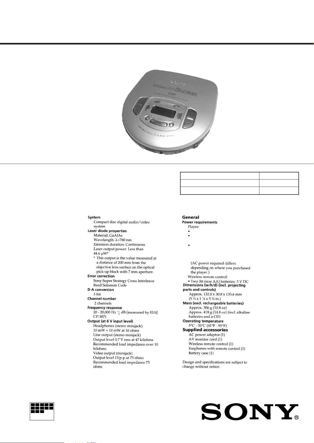
D-V55
SERVICE MANUAL
Ver 1.0 1999.05
SPECIFICATIONS
E Model
Chinese Model
Model Name Using Similar Mechanism NEW
CD Mechanism Type CDM-2901ABA
Optical Pick-up Type DAX-01A2
Two LR6 (size AA) batteries:3VDC
Battery case (External Batteries):
Two LR6 (size AA) batteries:3VDC
AC power adaptor (DC IN 6V jack):
220-230 V, 50/60Hz
220 V, 50Hz
220 V, 50/60Hz
MICROFILM
PORTABLE VIDEO CD PLAYER

TABLE OF CONTENTS
Specifications ........................................................................... 1
1. SERVICING NOTE....................................................... 3
2. GENERAL
Location and Function of Controls .................................... 4
3. DISASSEMBLY
3-1. Cabinet (Lower) Sub ASSY ....................................... 6
3-2. Lid Sub ASSY, Switch Unit........................................ 6
3-3. MPEG Board .............................................................. 7
3-4. MD ASSY, IR Board .................................................. 7
3-5. Main Board ................................................................. 8
3-6.Turn Table Motor ASSY (Spindle) (M902),
Optical Pick-up (DAX-01A2),
Sled Motor ASSY (M901) .......................................... 8
4. SERVICE MODE (TEST MODE)
4-1. How to Enter the Test Mode ....................................... 9
4-2. How to Release the Test Mode ................................... 9
4-3. Each Key Function in Test Mode ............................... 9
5. ELECTRICAL ADJUSTMENTS
5-1. Precautions for Adjustment ...................................... 10
5-2. Before Beginning Adjustment .................................. 10
5-3. Tracking Balance Check........................................... 10
5-4. Focus Bias Check ......................................................11
6. DIAGRAMS
6-1. Explanation of IC Terminals..................................... 12
6-2. Block Diagram.......................................................... 19
6-3. Printed Wiring Boards (Main Section) ..................... 23
6-4. Schematic Diagram (Main Section) ......................... 27
6-5. Schematic Diagram (MPEG Section)....................... 34
6-6. Printed Wiring Boards (MPEG Section) .................. 37
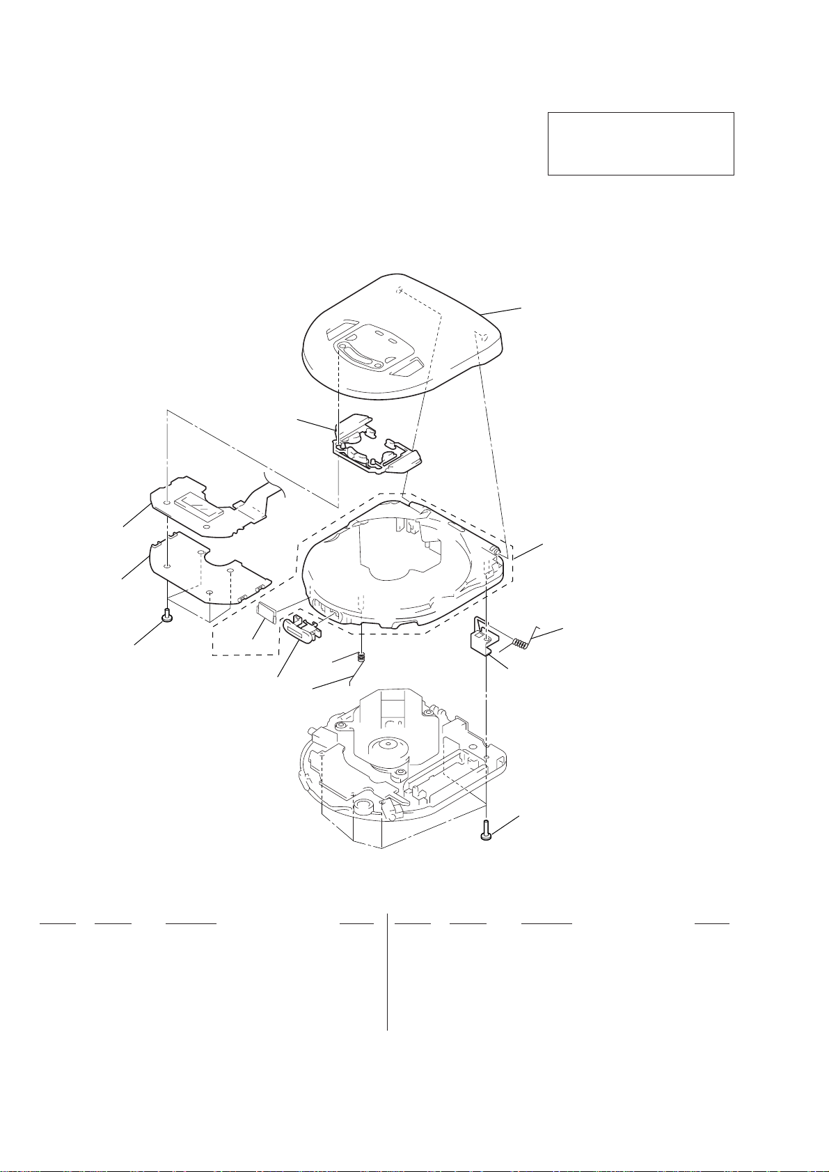
7. EXPLODED VIEWS
7-1. Cabinet (Upper) Section ........................................... 42
7-2. Cabinet (Lower) Section........................................... 43
7-3. Optical Pick-up Section (CDM-2901ABA) ............. 44
8. ELECTRICAL PARTS LIST ................................45
Flexible Circuit Board Repairing
• Keep the temperature of the soldering iron around 270°C during
repairing.
• Do not touch the soldering iron on the same conductor of the
circuit board (within 3 times).
• Be careful not to apply force on the conductor when soldering or
unsoldering.
Notes on chip component replacement
• Never reuse a disconnected chip component.
• Notice that the minus side of a tantalum capacitor may be damaged by heat.
SAFETY-RELATED COMPONENT WARNING!!
COMPONENTS IDENTIFIED BY MARK ! OR DOTTED LINE WITH
MARK !ON THE SCHEMATIC DIAGRAMS AND IN THE PARTS
LIST ARE CRITICAL TO SAFE OPERATION.
REPLACE THESE COMPONENTS WITH SONY PARTS WHOSE
PART NUMBERS APPEAR AS SHOWN IN THIS MANUAL OR IN
SUPPLEMENTS PUBLISHED BY SONY.
DANGER
Invisible laser radiation when open and interlock failed or defeated.
Avoid direct exposure to beam.
CAUTION
Use of controls or adjustments or performance of procedures other than
those specified herein may result in hazardous radiation exposure.
This Compact Disc player is
classified as a CLASS 1 LASER
product.
The CLASS 1 LASER
PRODUCT label is located on the
bottom exterior.
– 2 –

SECTION 1
4
3
2
1
5
6
4
3
2
1
5
6
1
5
10
11
20
B
C
E
B
C
E
BCE
BCE
BCE
R532
C525
C526
R751
C518
D501
C516
R544
L506
R518
IC501
R520
R531
R522
R542
R514
C530
C507
R515
R513
R525
C522
C529
R512
R516
R543
C502
Q504
R510
Q506
Q502
R509
C509
R506
R554
R528
R507
R511
R521
R519
R517
R526
Q501
C519
R523
Q503
Q507
C508
R527
TP512
TP520
TP534
TP540
TP537
TP531
TP536
TP524
TP535(RFO)
TP522
(FE)
TP523
(TE)
TP508
(VC)
TP521
TP752
TP810
TP809
TP530
TP525
15
TP524
digital voltmeter
TP520
SERVICING NOTE
NOTES ON HANDLING THE OPTICAL PICK-UP
BLOCK OR BASE UNIT
The laser diode in the optical pick-up block may suffer electrostatic breakdown because of the potential difference generated by
the charged electrostatic load, etc. on clothing and the human
body. During repair, pay attention to electrostatic breakdown and
also use the procedure in the printed matter which is included in
the repair parts.
The flexible board is easily damaged and should be handled with
care.
NOTES ON LASER DIODE EMISSION CHECK
The laser beam on this model is concentrated so as to be focused
on the disc reflective surface by the objective lens in the optical
pick-up block. Therefore, when checking the laser diode emission, observe from more than 30cm away from the objective lens.
Before Replacing the Optical pick-up Block
Please be sure to check thoroughly the parameters as per the
“Optical pick-up Block Checking Procedure” (Part No. : 9-960027-11) issued separately before replacing the optical Pick-up
block.
Note and specifications required to check are given below.
• FOK output : IC601 ((£ pin (FOK).
When checking FOK, remove the lead wire to disc motor.
• S curve P-to-P value : 1.2 – 2Vp-p IC501 !§ pin.
When checking S curve P-to-P value, remove the lead wire to
disc motor.
• RF signal P-to-P value : 0.5 – 0.9Vp-p
• Traverse signal P-to-P value : 1.2 – 2.0Vp-p
• The repairing grating holder is impossible.
Laser Diode Checking Methods
During normal operation of the equipment, emission of the laser
diode is prohibited unless the upper panel is closed while turning
ON the S804 (push switch type).
The following two checking methods for the laser diode are
operable.
AC2211397
current value
A : less than 48 mA
year
month
date
shift No.
line No.
version
3. Connect a digital voltmeter as shown in Fig. 1-2
4. Press the fl key.
5. Calculate the current value by the reading of the digital
voltmeter.
Reading of the digital voltmeter V ÷ 4.7 Ω = current value (A)
(Example) Reading of the digital voltmeter of 0.2256 V :
0.2256 V ÷ 4.7 Ω = 0.048 (A) = 48 mA
6. Check that the current value is within the following range.
• Current value of the label -11 mA(25˚C)
+5
Variation by temperature : 0.4mA / ˚C
Current increases with temperature increased.
Current decreases with temperature decreased.
If the current is more than the range above, there is a trouble
in the automatic power control circuit or the laser diode is in
deterioration.
If less than the range, a trouble exists in the automatic power
control circuit or the optical pick-up.
[MAIN BOARD] (SIDE B)
Method-1 (In the service mode or normal operation) :
Emission of the laser diode is visually checked.
1. Open the upper lid.
2. Push the S804 as shown in Fig. 1-1.
3. Press the fl key.
4. Check the object lens for confirming normal emission of the
laser diode. If not emitting, there is a trouble in the automatic
power control circuit or the optical pick-up. During normal
operation, the laser diode is turned ON about 2.5 seconds for
focus searching.
S804
Fig.1-1 Method to push S804
Method-2 (In the service mode or normal operation) :
Check the value of current flowing in the laser diode.
1. Remove the upper panel.
2. Read the current printed on the rear side of the optical pick-up.
(Print on the rear side of the optical pick-up)
Fig. 1-2 Digital Voltmeter Connecting Location
– 3 –

LOCATION AND FUNCTION OF CONTROLS
SECTION 2
GENERAL
This section is extracted from
instruction manual.
– 4 –

– 5 –
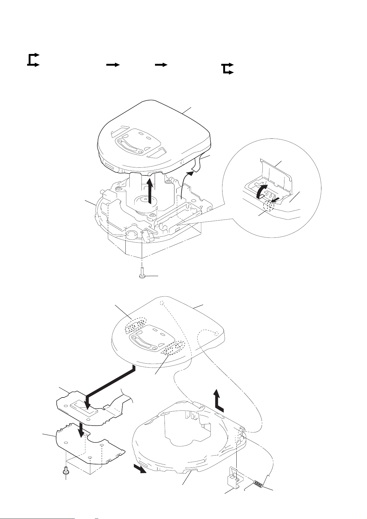
SECTION 3
DISASSEMBLY
r
The equipment can be removed using the following procedure.
Lid sub ASSY, Switch unit
Set Main board
Cabinet (Lower) sub ASSY
Note : Follow the disassembly procedure in the numerical order given.
3-1. CABINET (LOWER) SUB ASSY
Cabinet (lower) sub ASSY
MPEG board
MD ASSY, IR board
4
Lid sub ASSY
5
Flexible
board
Turn table motor ASSY (Spindle)
(M902), Optical pick-up (DAX-01A2),
Sled motor ASSY (M901)
2
Battery lid
3
3-2. LID SUB ASSY, SWITCH UNIT
6
Claws
Switch unit
8
1
Screws (B2x10)
6
Claws
Claw
Lid sub ASSY
Cover, lid
7
5
Screws (1.7x4)
1
OPEN
Cabinet (upper) sub ASSY
– 6 –
3
Bracket (spring)
2
4
Spring, torsion

3-3. MPEG BOARD
Y
Y
3-4. MD ASSY, IR BOARD
MPEG board
Cabinet (lower) sub ASS
1
CN601
6
IR board
2
CN502 (white)
1
Flexible board
CN501
3
CN503 (green)
4
CN504 (black)
MD ASSY
5
Cabinet (lower) sub ASS
– 7 –
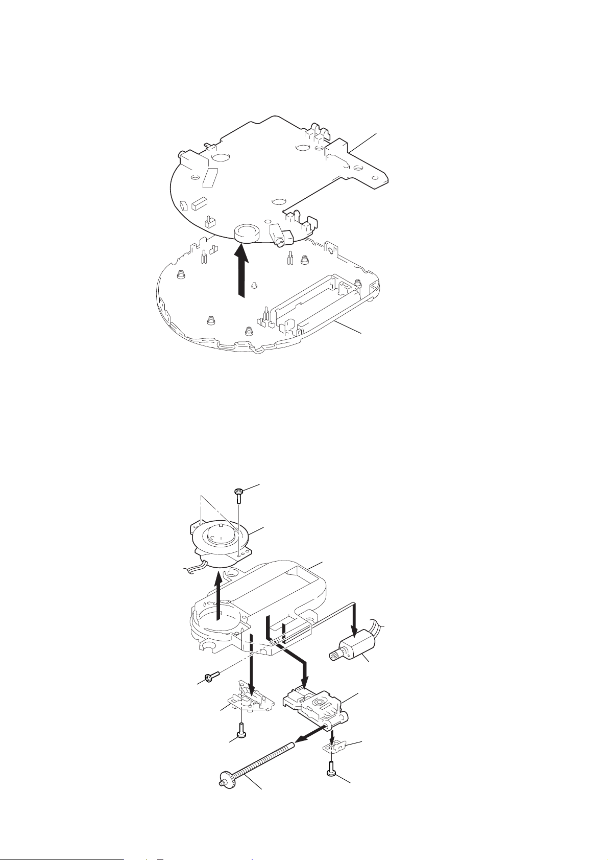
3-5. MAIN BOARD
Y
Main board
1
Cabinet (lower) sub ASS
3-6. TURN TABLE MOTOR ASSY (SPINDLE) (M902), OPTICAL PICK-UP (DAX-01A2),
SLED MOTOR ASSY (M901)
1
Screws (B1.7)
Turn table motor ASSY (Spindle) (M902)
Chassis
2
!º
Sled motor ASSY
(M901)
Optical pick-up
(DAX-01A2)
Rack
9
Screws
(+P1.4x2.5)
Spring, sled
3
Screw (B1.7x6)
4
8
5
7
Screw ASSY, Feed
– 8 –
6
Screw

SECTION 4
TAP801
(TEST)
CN801
CN501
Monitor IN
Video monitor
Video OUT (J901)
J901
SERVICE MODE (TEST MODE)
• In this set, there are two test modes; CD-DA Test Mode and
VIDEO CD Test Mode.
4-1. How to Enter the Test Mode
1. Disconnect external power (no current is applied to the set).
2. Bridge the TAP801 (TEST) on the MAIN Board with a solder.
(IC801 (∞ (TEST) pin is shorted to the ground.)
3. Connect the external power.
4. The CD-DA Test Mode is activated. (LCD display varies in 5ways, and its 5-way display is repeated.)
5. Before connecting external power in step 3, if π (STOP) key
was pressed, the mode is switched to VIDEO CD Test Mode.
(On the LCD, all segments are displayed, and the video monitor
becomes 100% white.)
4-2. How to Release the Test Mode
1. Always disconnect external power, and break the solder bridge
of TAP801 (TEST) on the MAIN Board.
2. Thus, the set become ready for normal operation.
4-3. Each key Function in Test Mode
1. CD-DA Test Mode
Switches Description
π Stop processing
Press once: Initialize, Average Correct
fl
(PLAY/PAUSE)
SELECT
±
(NEXT)
≠
(PREV)
ˆ
(RETURN)
ESP
REPEAT/
ENTER
+
MENU Raise K23** by one step after Tracking
–
MENU Lower K23** by one step after Tracking
* Coefficient of Focus Gain
** Coefficient of Tracking Gain
Press twice: Auto Focus
Press 3 times: Focus Auto Gain
Press 4 times: Tracking Auto Gain
Press 5 times: All Servo ON, Mute OFF
Repeat once more the processing currently
selected with fl (PLAY/PAUSE) key.
Move optical pick-up toward outside track
Move optical pick-up toward inside track
Turn off the Mute
Turn on/off the ESP (fast speed play, when
ON)
Tracking Gain up/normal switching
Raise K13* by one step after Focus Auto
Gain
Auto Gain
Lower K13* by one step after Focus Auto
Gain
Auto Gain
2. VIDEO CD Test Mode
Switches Description
π Go to CD-DA Test Mode
SELECT
– MAIN Board – (Side A)
Video system reset (return to 100% white
screen)
Fig.4-1 Test terminal location and connecting position
– 9 –

SECTION 5
A
ELECTRICAL ADJUSTMENTS
5-1. Precautions for Adjustment
1. Before beginning adjustment, set the equipment to service
mode.
After the completion of adjustment, be sure to reset the
service mode.
For more information, see “Service Mode (Test Mode)” on
page 9.
2. Perform adjustments in the order given.
3. Use YEDS-18 disc (Part No.: 3-702-101-01) unless otherwise
indicated.
4. Power supply voltage requirement: DC6 V
HOLD switch: OFF
VOLUME control: Minimum
RESUME switch: OFF
5-2. Before Beginning Adjustment
Set the equipment to service mode (See page 9) and check the
following. If there is an error, repair the equipment.
• Checking of the sled motor
1. Open the upper lid.
2. Press the ± and ≠ keys and check that the optical pickup can move smoothly without sluggishness or abnormal
noise in innermost periphery n outermost periphery n
innermost periphery.
± : The optical pick-up moves outwardly.
≠ : The optical pick-up moves inwardly.
• Checking of the Focus serching
1. Open the upper lid.
2. Press the fl key twice. (Focus searching operation is
activated continuously.)
3. Check the object lens of the optical pick-up for smooth up/
down motion without sluggishness or abnormal noise.
4. Press the π key.
Check that focus searching operation is deactivated. If not,
again press the π key slightly longer.
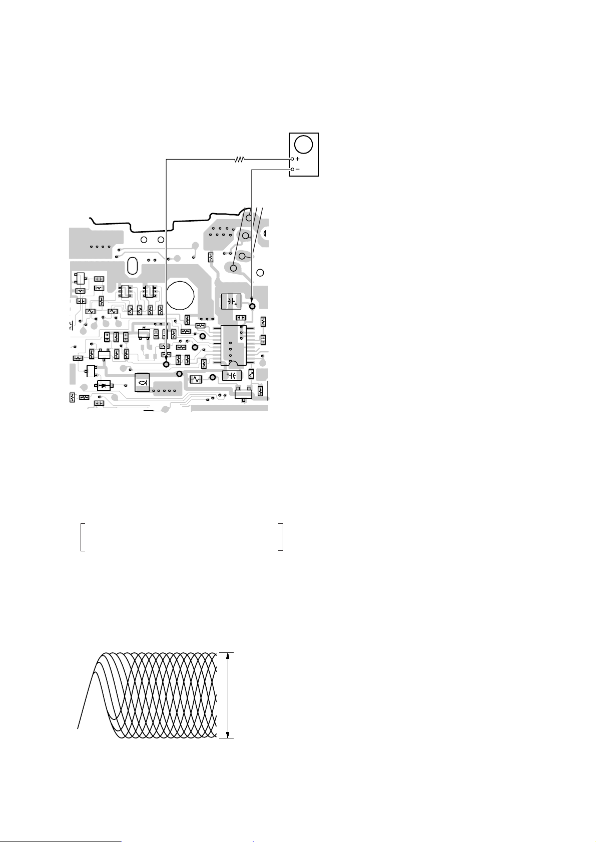
5-3. Tracking Balance Check
Condition:
• Hold the set in horizontal state.
Connection:
oscillscope
(DC range)
TP523(TE)
TP508(VC)
MAIN board (Side B)
B
C
E
C518
BCE
Q506
TP540
R522
R521
TP536
TP531
R554
R532
C522
C530
6
R528
5
4
TP525
R544
BCE
Q507
D501
Q503
R519
R526
R527
TP530
TP535(RFO)
R543
TP537
TP534
C525
1
2
3
C529
R542
L506
6
5
4
BCE
C526
Q502
R515
R518
Q504
1
2
3
C519
R525
R520
R531
C516
TP524
R513
R517
R523
TP809
TP810
R516
R511
R514
R510
R751
R512
TP520
TP523
TP522
C509
R509
11
(TE)
15
(FE)
20
TP521
C508
TP752
C502
IC501
E
5
1
R507
C
TP508
(VC)
10
B
Q501
R506
C507
TP512
Checking Method:
1. Connect the oscilloscope to TP523 (TE) and TP508 (VC) on
the MAIN board.
2. Set the equipment to service mode stop state. (See page 9.)
3. Press the fl key once.
4. Move the optical pick-up to the center by pressing the ±
and ≠ keys.
5. Put the disc (YEDS-18).
6. Press the fl key twice.
From focus searching, focus is turned ON while entering CL V
drawing-in mode. Tracking and sled are turned OFF.
7. Confirm that a waveform on the oscilloscope is vertically
symmetric against 0 V.
Note: Take long sweep time
for easy monitoring.
A
0 V
1.2 – 2 Vp-p
B
0 V
B
A=B A=B
8. Stop removing of the disc motor by pressing the π key.
9. After the completion of check, reset service mode. (See page
9.)
– 10 –
5-4. Focus Bias Check
Condition:
• Hold the set in horizontal state.
8. Stop revolving of the disc motor by pressing the π key.
9. After the completion of check, reset service mode.
(See page 9.)
Connection:
MAIN board (Side B)
C522
B
C
E
C518
BCE
Q506
TP540
R521
TP536
TP531
R554
R532
R522
C530
R528
TP525
R544
BCE
Q507
D501
6
5
4
R519
R543
C525
Q503
R526
R527
TP530
TP537
TP534
1
2
3
C529
R542
TP535(RFO)
L506
6
5
4
BCE
C526
TP535 (RFO)
Q502
1
2
3
R515
R518
Q504
C516
C519
R525
R520
TP524
R531
R513
R517
R523
TP809
TP810
R516
R510
TP508 (VC)
R751
C509
R511
(TE)
TP523
(FE)
TP522
R512
R514
TP520
TP521
R509
11
15
20
2k
TP752
C502
C508
Ω
5
IC501
1
R507
C
E
TP508
(VC)
10
B
Q501
C507
TP512
oscillscope
(AC range)
R506
Checking Method:
1. Connect the oscilloscope to TP535 (RFO) and TP508 (VC)
on the MAIN board.
2. Set the equipment to service mode stop state. (See page 9.)
3. Press the fl key once.
4. Move the optical pick-up to the center by pressing the ±
and ≠ keys.
5. Put the disc (YEDS-18).
6. Press the fl key four times.
From focus searching, focus is turned ON while
entering CLV drawing-in mode. Both tracking and
sled are turned ON.
7. Check the oscilloscope waveform is as shown below.
A good eye pattern means that the diamond shape (≈) in the
center of the waveform can be clearly distinguished.
RF SIGNAL REFERENCE WAVEFORM (EYE PATTERN)
VOLT/DIV : 200 mV (With the 10:1 probe in use)
TIME/DIV : 500 ns
RF level
0.5 – 0.9 Vp-p
To watch the eye pattern, set the oscilloscope to AC range and increase the vertical sensitivity of the oscilloscope for easy watching.
– 11 –

SECTION 6
DIAGRAMS
6-1. EXPLANATION OF IC TERMINALS
• MAIN BOARD (1/2) IC601 CXD2545Q
(DIGITAL SIGNAL PROCESSOR, FOCUS/TRACKING/SLED SERVO, EFM COMPARATOR)
Pin No. Pin name I/O Description
1 SRON O Sled servo drive PWM signal output terminal. Not used (open)
2 SRDR O Sled servo drive PWM signal (-) output to the MPC17A51VMEL (IC502).
3 SFON O Sled servo drive PWM signal output terminal. Not used (open)
4 TFDR O Tracking servo drive PWM signal (-) output to the MPC17A51VMEL (IC502).
5 TRON O Tracking servo drive PWM signal output terminal. Not used (open)
6 TRDR O Tracking servo drive PWM signal (+) output to the MPC17A51VMEL (IC502).
7 TFON O Tracking servo drive PWM signal output terminal. Not used (open)
8 FFDR O Focus servo drive PWM signal (+) output to the MPC17A51VMEL (IC502).
9 FRON O Focus servo drive PWM signal output terminal. Not used (open)
10 FRDR O Focus servo drive PWM signal (-) output to the MPC17A51VMEL (IC502).
11 FFON O Focus servo drive PWM signal output terminal. Not used (open)
12 VCOO O Oscillator circuit output terminal for analog PLL of the playback EFM.
13 VCOI I Oscillator circuit input terminal for analog PLL of the playback EFM.
14 TEST I Input terminal for the test (fixed at “L”).
15 DVSS – Ground terminal (digital system).
16 TES2 I Input terminal for the test (fixed at “L”).
17 TES3 I Input terminal for the test (fixed at “L”).
18 PDO O Charge-pump output terminal for analog PLL of the playback EFM. Not used (open)
19 VPCO O PLL charge-pump output terminal for the variable pitch. Not used (open)
20 VCKI I Master clock signal (16.9344 MHz) input from the D/A converter (IC322) for the variable pitch.
21 AVD2 – Power supply terminal (+3.3V) (analog system).
22 IGEN I Power supply terminal (+3.3V) (for operational amplifier).
23 AVS2 – Ground terminal (analog system).
24 ADIO I Input terminal for the A/D converter. Not used (open)
25 RFC O Output terminal of the operational amplifier. Not used (open)
26 RFDC I RF signal (DC level) input terminal for the digital servo process.
27 TE I Tracking error signal input from the CXA1791N (IC501).
28 SE I Sled error signal input from the CXA1791N (IC501).
29 FE I Focus error signal input from the CXA1791N (IC501).
30 VC I Middle point voltage (+1.65V) input from the CXA1791N (IC501).
31 FILO O Filter output terminal for master clock of the playback master PLL.
32 FILI I Filter input terminal for master clock of the playback master PLL.
33 PCO O Phase comparison output terminal for master clock of the playback EFM master PLL.
34 CLTV I Internal VCO control voltage input of the playback master PLL.
35 AVS1 – Ground terminal (analog system).
36 RFAC I RF signal (AC level) input terminal for the EFM demodulator.
37 BIAS I Constant current input terminal of the playback EFM asymmetry circuit.
38 ASYI I Playback EFM asymmetry comparator voltage input terminal.
39 ASYO O Playback EFM full-swing output terminal.
40 AVD1 – Power supply terminal (+3.3V) (analog system).
41 DVDD – Power supply terminal (+3.3V) (digital system).
42 ASYE I Playback EFM asymmetry circuit on/off selection input terminal (fixed at “H”).
43 PSSL I Audio data output mode selection input terminal (fixed at “L”).
44 WDCK O Word clock signal (88.2 kHz) output terminal. Not used (open)
45 LRCK O
L/R sampling clock signal (44.1 kHz) output to the D-RAM controller (IC681) and
MPEG audio/video decoder (IC701).
– 12 –

Pin No. Pin name I/O Description
DA16 output when PSSL=“H”, 48-bit slot serial data output when PSSL=“L”
46 DATA O
47 BCLK O
48 64 DATA O
49 64 BCLK O
50 64 LRCK O
51 GTOP O
52 XUGF O
53 XPLCK O
54 GFS O
55 RFCK O
56 C2PO O
57 XRAOF O
58 MNT3 O
59 MNT2 O
60 MNT1 O
61 MNT0 O
62 XTAI I Master clock signal (16.9344 MHz) input from the D/A converter (IC322).
63 XTAO O Master clock output terminal (16.9344 MHz). Not used (open)
64 XTSL I Master clock selection input terminal (fixed at “L”).
65 DVSS – Ground terminal (digital system).
66 FSTI I 2/3 divider input terminal of pins ^™ (XATI) and ^£ (XTAO).
67 FSTO O 2/3 divider output terminal of pins ^™ (XATI) and ^£ (XTAO).
68 C4M O 4.2336 MHz clock signal output terminal. Not used (open)
69 C16M O 16.9344 MHz clock signal output terminal. Not used (open)
70 MD2 I Digital out on/off control signal input terminal Fixed at “H” in this set.
71 DOUT O Digital signal (for coaxial out and optical out) output terminal. Not used (open)
72 EMPH O Emphasis control signal output terminal. Not used (open)
73 WFCK O Write frame clock signal output terminal. Not used (open)
74 SCOR O
75 SBSO O Sub-code P-W serial data output terminal. Not used (open)
(PSSL (pin $£)=fixed at “L”) Serial data output to the D-RAM controller (IC681) and
MPEG audio/video decoder (IC701).
DA15 output when PSSL=“H”, 48-bit slot bit clock signal output when PSSL=“L”
(PSSL (pin $£)=fixed at “L”) Bit clock signal (2.8224 MHz) output to the D-RAM
controller (IC681) and MPEG audio/video decoder (IC701).
DA14 output when PSSL=“H”, 64-bit slot serial data output when PSSL=“L”
(PSSL (pin $£)=fixed at “L”). Not used (open)
DA13 output when PSSL=“H”, 64-bit slot bit clock signal output when PSSL=“L”
(PSSL (pin $£)=fixed at “L”). Not used (open)
DA12 output when PSSL=“H”, 64-bit slot L/R sampling clock signal output when
PSSL=“L” (PSSL (pin $£)=fixed at “L”). Not used (open)
DA11 output when PSSL=“H”, GTOP signal output when PSSL=“L”
(PSSL (pin $£)=fixed at “L”). Not used (open)
DA10 output when PSSL=“H”, XUGF signal output when PSSL=“L”
(PSSL (pin $£)=fixed at “L”). Not used (open)
DA09 output when PSSL=“H”, XPLCK signal output when PSSL=“L”
(PSSL (pin $£)=fixed at “L”). Not used (open)
DA08 output when PSSL=“H”, GFS (guard frame sync) signal output when PSSL=“L”
(PSSL (pin $£)=fixed at “L”). Not used (open)
DA07 output when PSSL=“H”, RFCK (read frame clock) signal output when PSSL=“L”
(PSSL (pin $£)=fixed at “L”). Not used (open)
DA06 output when PSSL=“H”, C2PO signal output when PSSL=“L”
(PSSL (pin $£)=fixed at “L”) C2PO signal output to the D-RAM controller (IC680)
and MPEG audio/video decoder (IC901).
DA05 output when PSSL=“H”, XRAOF (RAM over flow) signal output when PSSL=“L”
(PSSL (pin $£)=fixed at “L”). Not used (open)
DA04 output when PSSL=“H”, MNT3 (monitor 3) signal output when PSSL=“L”
(PSSL (pin $£)=fixed at “L”). Not used (open)
DA03 output when PSSL=“H”, MNT2 (monitor 2) signal output when PSSL=“L”
(PSSL (pin $£)=fixed at “L”). Not used (open)
DA02 output when PSSL=“H”, MNT1 (monitor 1) signal output when PSSL=“L”
(PSSL (pin $£)=fixed at “L”). Not used (open)
DA01 output when PSSL=“H”, MNT0 (monitor 0) signal output when PSSL=“L”
(PSSL (pin $£)=fixed at “L”). Not used (open)
Sub-code sync (S0+S1) detection signal output to the D-RAM controller (IC681) and
system controller (IC801).
– 13 –

Pin No. Pin name I/O Description
76 EXCK I Sub-code P-W serial data reading clock signal input terminal. Not used (fixed at “L”)
77 SUBQ O Sub-code Q data signal output to the system controller (IC801).
78 SQCK I Sub-code Q data reading clock signal input from the system controller (IC801).
79 MUTE I Mute signal input terminal. Fixed at “L” in this set
80 SENS O Internal status (SENSE) signal output to the system controller (IC801).
81 XRST I
______
82 DIRC I 1-track jump mode input terminal Not used (fixed at “H”)
83 SCLK I Sense serial data reading clock signal input from the system controller (IC801).
84 DFSW I Defect on/off select signal input terminal. Not used (fixed at “L”)
85 ATSK I Input terminal for the anti-shock. Not used (fixed at “L”)
86 DATA I Serial data input from the system controller (IC801).
87 XLAT I Serial data latch pulse signal input from the system controller (IC801).
88 CLOK I Serial data transfer clock signal input from the system controller (IC801).
89 COUT O Track number count signal output terminal. Not used (open)
90 DVDD – Power supply terminal (+3.3V) (digital system).
91 MIRR O Mirror detection signal output terminal. Not used (open)
92 DFCT O Defect signal output terminal. Not used (open)
93 FOK O Focus OK signal output terminal. Not used (open)
94 FSW O Selection signal output terminal of the output filter for spindle motor. Not used (open)
95 MON O Spindle motor on/off control signal output terminal. Not used (open)
96 MDP O Spindle servo control signal output.
97 MDS O Spindle servo control signal output.
98 LOCK O GFS is sampled by 460 Hz. “H” output when GFS is “H” Not used (open)
99 SSTP I
100 SFDR O Sled servo drive PWM signal (+) output to the MPC17A51VMEL (IC502).
Reset signal input from the system controller (IC801) “L”: reset
For several hundreds msec. after the power supply rises,“L” is input, then it changes to “H”
Detection input from the sled limit-in detect switch (S901). The optical pick-up is inner
position when “H”
– 14 –

• MAIN BOARD IC801 MSM65354-418GS-BK4 (SYSTEM CONTROLLER, LCD DRIVER, KEY CONTROL)
Pin No. Pin name I/O Description
1-4 COM1-4 O Common drive signal output to the liquid crystal display.
5-19 SEG0-14 O Segment drive signal output to the liquid crystal display.
20-36 NC – Not used (open).
37 AGND – Ground terminal (analog system).
38 DC IN JACK I DC IN 6V jack (J801) detection input terminal. “L”: plug in
39 DOOR OPEN I
40 KEY IN1 I Key input terminal (A/D input).
41 XRM KEY IN I Remote control key input terminal (A/D input).
42 DC CHK I DC in voltage detection input terminal (A/D input) Also used for DC IN detection
43 NTSC/PAL I Video system select switch (S803) input terminal “L”: NTSC, “H”: PAL
44 BATT CHK I Battery check terminal.
45 KEY IN2 I Key input terminal (A/D input).
46 VRH I Reference voltage input terminal (+3.3V) (for A/D converter).
47 AVDD – Power supply terminal (+3.3V) (analog system).
48 DBB CTL1 O
49 AU-MUTE O Analog line mute control signal output terminal . “H”: mute on
50 XAU-RESET O Reset signal output to the CXD2545Q (IC601) and D-RAM controller (IC681). “L”: reset
51 XV-RESET O
52 HOLD I HOLD switch (S802) input terminal. “L”: hold off, “H”: hold on
53 RESUME I RESUME switch (S801) input terminal. “L”: resume off, “H”: resume on
54 XDSPLT O Serial data latch pulse signal output to the CXD2545Q (IC601).
55 XDACLT O Serial data latch pulse signal output to the D/A converter (IC322).
56 V-POWER O Video CD system power supply on/off control signal output terminal. “L”: power on
57 AU-POWER O Audio CD system power supply on/off control signal output terminal. “L”: power on
58 ESP-POWER O Control signal output to the ESP (Electronic Shock Protection) circuit.
59 TRVCTL O Tracking gain control signal output terminal.
60 TRV3 O
61 TRV2 O
62 TRV1 O
63 TRV0 O
64 XSOE O Serial data output enable signal output to the D-RAM controller (IC681).
65 DSP-SUBQ I Sub-code Q data signal input from the CXD2545Q (IC601).
66 DSP-SBQCLK O Sub-code Q data reading clock signal output to the CXD2545Q (IC601).
67 REMOTE I Sircs remote control signal input from the remote control receiver (IC1).
68 DSP-DATA O Serial data output to the CXD2545Q (IC601) and D/A converter (IC322).
69 DSP-SENS I Internal status (SENSE) signal input from the CXD2545Q (IC601).
70 DSP-CLK O Serial data transfer clock signal output to the CXD2545Q (IC601) and D/A converter (IC322).
71 DSP-SNSCLK O Sense serial data reading clock signal output to the CXD2545Q (IC601).
72 VDD – Power supply terminal (+3.3V) (digital system).
73 BEEP O Beep sound drive signal output terminal.
74 C2PO O C2PO signal control output to the D-RAM controller (IC681). “L”: stop mode, “H”: searching
75 ESP-CLK O Serial data transfer clock signal output to the D-RAM controller (IC681).
____________
__________
______
CD lid open/close detection switch (S804) input terminal The stop status is reset with the
falling edge of input signal. “H”: CD lid open, “L”: CD lid close
MEGA BASS on/off control signal output to the BA3574BFS (IC361).
“L”: MEGA BASS on (level-1 and level-2)
Reset signal output to the MPEG audio/video decoder (IC701) and video encoder (IC721).
“L”: reset
Tracking balance control signal output terminal.
– 15 –

Pin No. Pin name I/O Description
76 ESP-DATA O Serial data output to the D-RAM controller (IC681).
77 ESP-LT O Serial data latch pulse signal output to the D-RAM controller (IC681).
78 ESP-SENSE I Sense serial data input from the D-RAM controller (IC681).
79 XLASERCTL O Laser diode on/off control signal output to the CXA1791N (IC501). “L”: laser on
80 DSP-SCOR I Sub-code sync (S0+S1) detection signal input from the CXD2545Q (IC601).
81 OSC1 O Main system clock output terminal (4.19 MHz).
82 OSC0 I Main system clock input terminal (4.19 MHz).
83 GND – Ground terminal (digital system).
84 XT I Sub system clock input terminal. Not used (fixed at “L”)
85 XTO O Sub system clock output terminal. Not used (open)
86 A-SELECT O
87 XIRCTL O Power supply on/off control signal for the remote control receiver (IC1). “L”: power on
88 SYS XMT RQ O Communication request signal output to the MPEG audio/video decoder (IC701).
89 SYS RCV RDY O Ready signal output to the MPEG audio/video decoder (IC701).
90 MPG XMT RQ I Communication request signal input from the MPEG audio/video decoder (IC701).
91 ESS-DATAO O Serial data output to the MPEG audio/video decoder (IC701).
92 ESS-DATAI I Serial data input from the MPEG audio/video decoder (IC701).
93 ESS-CLK O Serial data transfer clock signal output to the MPEG audio/video decoder (IC701).
94 RESET I
95 TEST I
96 DBB CTL2 O
97 VDDL –
98 VDD1 –
99 VDD2 –
100 VDD3 –
____________
______
_____
Selection signal output to the DATA, BCLK, LRCK signal select switch (IC321) .
“L”: CD play, “H”: video CD play
System reset signal input from the reset signal generator (IC802). “L”: reset
For several hundreds msec. after the power supply rises, “L” is input, then it changes to “H”
Service mode setting terminal. The stop status is reset with the falling edge of input signal
“L”: service mode, Normally: “H”
MEGA BASS level control signal output to the BA3574BFS (IC361) .
“L”: MEGA BASS level-1, “H”: MEGA BASS level-2
Power supply output for the liquid crystal display bias.
– 16 –

• MPEG BOARD IC701 ES3210 (MPEG AUDIO/VIDEO DECODER)
Pin No. Pin name I/O Description
1 VCC – Power supply terminal (+3.3V).
2 DRAS B O Row address strobe signal output to the D-RAM (IC703) . “L” active
3 DWE B O Write enable signal output to the D-RAM (IC703). “L” active
4 – 12 MA0 – 8 O Address signal output to the D-RAM (IC703).
13 – 28 DBUS0 – 15 I/O Two-way data bus with the D-RAM (IC703).
29 RESET B I Reset signal input from the system controller (IC801). “L”: reset
30 VSS – Ground terminal.
31 VCC – Power supply terminal (+3.3V).
32 – 39 YUV0 – 7 O
40 VSSCN B O Vertical synchronous signal output to the video encoder (IC721).
41 HSSCN B O Horizontal synchronous signal output to the video encoder (IC721).
42 CLK I System clock signal input terminal Not used (open).
43 PCLK2XSCN I System clock signal (27 MHz) input from the video encoder (IC721).
44 PCKLQSCN O Pixel clock qualifier output for the screen video interface Not used (open).
45 AUX0 O Sub control signal output terminal Not used (open).
46 AUX1 I Serial data input from the system controller (IC801).
47 AUX2 O Serial data output to the system controller (IC801).
48 AUX3 O NTSC/PAL mode selection signal output to the video encoder (IC721). “L”: NTSC, “H”: PAL
49 AUX4 I C2PO signal input from the CXD2545Q (IC601).
50 VSS – Ground terminal.
51 VCC – Power supply terminal (+3.3V).
52 AUX6 O Communication request signal output to the system controller (IC801).
53 AUX5 I Ready signal input from the system controller (IC801).
54 AUX7 I Communication request signal input from the system controller (IC801).
55 – 62 LD0 – 7 I Data input from the program ROM (IC702).
63 LWR B O Write enable signal output terminal. “L” active Not used
64 LOE B O Output enable signal output to the program ROM (IC702). “L” active
65 LCS3 B O Chip select signal output to the program ROM (IC702). “L” active
66 LCS1 B I Serial data transfer clock signal input from the system controller (IC801). “L” active
67 LCS0 B O Chip select signal output terminal. “L” active Not used (open)
68 – 79 LA0 – 11 O Address signal output to the program ROM (IC702).
80 VSS – Ground terminal.
81 VPP – Power supply terminal (+5V) (digital system).
82 – 87 LA12 – 17 O Address signal output to the program ROM (IC702).
88 AUDIOCLK I Audio master clock signal (16.9344 MHz) input from the D/A converter (IC322).
89 AOUT O Audio interface serial data output to the D/A converter (IC322).
90 TBCK O Bit clock signal (2.8224 MHz) output to the D/A converter (IC322).
91 ATFS O L/R sampling clock signal (44.1 kHz) output to the D/A converter (IC322).
92 DOE B O Output enable signal output to the D-RAM (IC703). “L” active
93 AIN I Audio interface serial data input terminal. Not used (open)
94 RBCK I Audio interface bit clock signal (2.8224 MHz) input terminal. Not used (open)
95 ARFS I Audio interface L/R sampling clock signal (44.1 kHz) input terminal. Not used (open)
96 TDMCLK I Bit clock signal (2.8224 MHz) input from the CXD2545Q (IC601).
97 TDMDR I Serial data input from the CXD2545Q (IC601).
98 TDMFS I L/R sampling clock signal (44.1 kHz) input from the CXD2545Q (IC601).
99 DCAS B O Column address strobe signal output to the D-RAM (IC703). “L” active
100 VSS – Ground terminal.
_______
_______
________
Video data output to the video encoder (IC721).
(YUV; Y: luminance signal, UV: Screen video interface chrominance data bus)
______
_______
_______
_______
_______
______
_______
– 17 –

• MPEG BOARD IC721 TC90A07U (VIDEO ENCODER)
Pin No. Pin name I/O Description
1 MIFH I Horizontal synchronous signal input from the MPEG audio/video decoder (IC701).
2 MIFFL I Vertical synchronous signal input from the MPEG audio/video decoder (IC701).
3 MIFFR O Frame synchronous signal output terminal. Not used (open)
4 VBLNKI I Video blanking signal input terminal. “L”: blanking
5 VDD – Power supply terminal (+3.3V) (digital system).
6 GND – Ground terminal (digital system).
7 YCDI0 I 8 bit pixel data (LSB) input from the MPEG audio/video decoder (IC701).
8- 13 YCDI1 – YCDI6 I 8 bit pixel data input from the MPEG audio/video decoder (IC701).
14 YCDI7 I 8 bit pixel data (MSB) input from the MPEG audio/video decoder (IC701).
15 MODE I
16 VBLNKO O Video blanking signal output terminal.
17 VDD – Power supply terminal (+3.3V) (digital system).
18 GND – Ground terminal (digital system).
19 CLPF I
20 BF O Burst flag pulse output terminal. Not used (open)
21 BLK O Blanking signal output terminal. Not used (open)
22 FLD O
23 BIAS2 – Connect a capacitor for the D/A converter bias.
24 BIAS1 – Connect a capacitor for the D/A converter bias.
25 VREF I Reference voltage input terminal (for D/A converter).
26 AGND – Ground terminal (analog system for D/A converter).
27 YOUT O Analog Y signal (luminance signal) output terminal. Not used (open)
28 AVCC – Power supply terminal (+3.3V) (analog system for D/A converter).
29 COUT O Analog C signal (chroma signal) output terminal. Not used (open)
30 AGND – Ground terminal (analog system for D/A converter).
31 CVOUT O Analog composite video signal output terminal.
32 AVCC – Power supply terminal (+3.3V) (analog system for D/A converter).
33 CSYNC O Composite synchronous signal output terminal. Not used (open)
34 HSYNC O Horizontal synchronous signal output terminal. Not used (open)
35 VSYNC O Vertical synchronous signal output terminal. Not used (open)
36 TMS3 I Mode setting terminal. Normally fixed at “H”
37 VDD – Power supply terminal (+3.3V) (digital system).
38 CK27I I System clock input terminal (27 MHz).
39 XO O System clock output terminal (27 MHz).
40 GND – Ground terminal (digital system).
41 TMS2 I Mode setting terminal. Normally fixed at “H”
42 CK27O O System clock signal (27 MHz) output to the MPEG audio/video decoder (IC701).
43 TMS1 I Reset signal input from the system controller (IC801) . “L”: reset
44 TMS0 I Video output mode setting terminal. “L”: normal output mode, “H”: color bar output mode
NTSC/PAL mode selection signal input from the MPEG audio/video decoder (IC701).
“L”: NTSC, “H”: PAL
Low-pass filter on/off control signal input for the internal CbCr. “L”: on, “H”: off
Fixed at “L” in this set
Field discrimination signal output terminal. “L”: odd number field, “H”: even number field
Not used (open)
– 18 –

6-2. BLOCK DIAGRAM
D-V55
– 19 – – 20 – – 22 –– 21 –
• Signal path.
J : CD
L : VIDEO

D-V55
r
Semiconductor Location
Ref. No. Location Ref. No. Location
D101 B-17
D102 G-16
D201 B-17
D202 H-16
D301 H-16
D302 H-16
IC601 C-12
IC602 E-17
IC681 C-17
IC682 D-3
IC801 F-13
IC802 D-13
D351 E-17
D361 F-17
D401 F-11
D402 G-11
Q101 C-17
Q201 C-17
Q351 E-17
D404 E-12
D405 F-9
Q352 E-17
Q353 E-17
D411 E-4
D412 E-16
D421 F-16
Q361 F-17
Q362 G-16
Q363 G-16
D422 F-4
D501 C-14
Q412 E-4
Q413 F-9
D601 D-12
D681 D-18
D682 D-16
Q421 F-4
Q422 F-4
Q501 C-15
D801 E-12
Q502 B-14
Q503 B-14
IC1 A-1
IC321 D-18
IC322 E-18
IC361 F-17
IC411 F-16
IC421 F-16
IC501 B-15
IC502 C-15
Q504 B-14
Q505 B-13
Q506 C-14
Q507 C-14
Q601 D-12
Q801 E-14
Q802 F-14
Q812 E-13
IC503 C-14
IC504 D-14
Note:
• X : parts extracted from the component side.
®
•
: Through hole.
• b : Pattern from the side which enables seeing.
(The other layers' patterns are not indicated.)
Caution:
Pattern face side: Parts on the pattern face side seen from the
(Side B) pattern face are indicated.
Parts face side: Parts on the parts face side seen from the
(Side A) parts face are indicated.
6-3. PRINTED WIRING BOARDS (MAIN SECTION)
1 2 3 4 5 6 7 8 9 10 11 12 13 14 15 16 17 18 19
[IR BOARD]
A
B
(SIDE A)
C1
1
2
IC1
4
3
1-674-189-
11
(11)
S802
HOLD
[IR BOARD]
(SIDE B)
C
D
E
F
G
H
I
M901
SLED
MOTOR
S901
(LIMIT)
MPEG
BOARD
CN901
(page 38)
M902
SPINDLE
MOTOR
02
TP2
M
A
M
TP3
TP1
1-674-189-
ORG
BLK
GRY
GRY
BLK
RED
11
(11)
TAP802
C752
RED
WHT
CN802
C330
BLK
RED
1
WHT
BLK
14
FB804
C619
C364
J901
[MAIN BOARD] (SIDE A)
S801
RESUME
OFF
TP529
TP518
OFF
ON
BLK
Q412
TAP501
TP519
12
GRY
GRY
D
C429
T421
CN504
S
R429
C426
CN501
1
BLK
12
CN503
D422
SDG
6
5
RED
Q422
TP526
C683
913
18
20
C366
10
15
C328
24
23
IC682
22
5
5
L411
C414
2
1
C418
C423
TP528
ORG
1
12
CN502
26
D411
R426
C428
G
C417
B
C
E
R425
Q421
10
1
C427
TAP502
TP527
TP532
14
ON
OPTICAL PICK-UP
BLOCK
DAX-01A2
SWITCH UNIT
LIQUID CRYSYAL DISPLAY
PLAY MODE
REPEAT/
TAP801
(TEST)
EXTERNAL
BATTERY
DRY BATTERY
SIZE “AA”
(IEC DESIGNATION LR6)
2PCS‚ 3V
J401
DC IN 6V
CN801
1
5
15
23
C809
2
C808
10
20
24
D405
BCE
Q413
TP405
ENTER
ESP
MEGA
BASS
RETURN MENU- MENU+ SELECT
1-674-190-
11
(11)
TP301
[MAIN BOARD] (SIDE B)
50
TP625
TP623
TP613
D401
55
TP622
TP618
TP616
TP612
TP611
D404
C605
C602
TP825
C401
51
60
65
70
75
80
81
TP403
TP817
Q601
FB805
TP815
FB802
TP827
TP835
TP620
L402
TP624
TP621
TP619
TP617
TP615
TP614
TB402
TB401
L401
D402
C613
45
85
R602
TP603
BCE
X801
TP404
R804
TP826
TP833
R803
TP831
C601
C801
TAP602
TAP601
40
IC601
90
TP602
TP604
TP802
TP816
R801
R824
TP830
C616
R607
TP605
C802
FB801
TP801
TP818
100
R802
C612
35
R608
95
TP606
TP607
R601
D601
C603
81
85
90
TP803
95
TP821
TP822
TAP603
R610
C615
R609
C609
C611
R605
R604
R613
R614
R616
R618
C806
C604
R621
C608
C606
R611
R617
R551
C534
R546
4
1
C816
L601
L602
C607
R615
C617
R541
R556
R548
R823
C805
R820
R612
R539
C528
R825
Q812
R530
TP538
C527
C533
TP517
BCE
C535
R550
C804
TP609
80
31
R606
25
20
15
10
100
TP601
C803
L801
5
R620
TP608
5
8
D801
30
1
TP610
R603
IC802
R619
IC801
511015202530
TP829
TP823
TP824
TP828
TP832
TP837
TP839
Q505
R524
C518
R536
1
4
1
4
55 5160657075
B
C
E
R553
Q506
R537
R805
R826
R521
R557
R519
TP536
TP531
R554
BCE
TP540
R532
IC503
IC504
R806
C522
R522
C530
BCE
50
45
40
35
31
TP838
6
5
R528
4
TP525
Q507
D501
8
5
8
5
Q503
R526
R527
R544
R543
TP537
TP534
C525
R535
R540
R549
TP804
R811
R813
C807
TP834
Q802
Q502
6
1
5
2
4
3
R515
R518
Q504
TP530
BCE
C529
R558
R529
R542
TP535(RFO)
L506
C526
R555
C532
R547
R810
BCE
BCE
TP808
R821
TP807
TP836
PAL
1
2
3
C519
R525
R531
R538
TP539
TP806
R812
AUDIO/VIDEO
OUT
TP809
TP810
R751
R511
C516
R516
R513
R517
R520
TP524
R534
S803
S803
R545
R807
R817
R822
R512
R514
R523
TP520
R510
TP533
R814
RECHARGEABLE BATTRY
C512
C536
L504
L502
C503
Q801
TP805
NTSC
DRY BATTERY
SIZE “AA”
(IEC DESIGNATION LR6)
2PCS‚ 3V
(NICKEL-CADMIUM)
BP-DM10/DM20
2.4V
C509
R509
11
(TE)
TP523
15
(FE)
20
TP522
C514
C520
C510
TP521
19
20
25
30
35
36
TP401
TP752
C502
C508
TP508
(VC)
5
IC501
1
R507
C
E
IC502
10
C507
B
Q501
R508
TP422
R506
TP512
TP411
IC421
R505
R501
18
15
10
5
1
R402
R401
R421
TP513
TP505
R404
C416
C424
4
D421
TP509
2
TP507
TP514
R504
R503
TP511
R502
C506
C511
TP504
TP501
TP503
C515
C513
L505
C523
C504
TP642
R415
C413
C411
R403
2
1
R418
C415
IC411
5
4
R428
C430
C422
R423
1
5
C421
R427
R424
TB404
1-674-190-
TP510
TP506
C505
TP502
TP516
C517
R413
TAP411
C425
TP365
TB403
C521
D412
D202
(11)
R815
L503
C501
TP626
TP414
TP421
TP412
R422
TAP421
Q363
BCE
TP303
11
TP101
FB101
FB751
TP201
FB201
R816
FB803
L501
TP515
FB682
TP644
C412
R414
R416
R417
C206
R362
BCE
D102
R753
C810
34
TP683
35
40
44
C684
Q351
TP351
C351
C106
R207
10
R365
FB202
D301
D302
FB806
TP751
C101
R101
R754
D201
C201
TP812
R201
R105
TP811
TP813
R205
TP682
TP681
33 30 25 23
IC681
5
1
D682
TP629
TP631
TP639
TP637
C352
R352
3
BCE
R351
2
D351
R353
2
1
3
Q361
6
5
R107
4
C365
C375
1
IC361
5
C372
C371
C370
R363
R364
Q362
TP364
FB301
R819
C812
FB807
FB808
R818
TP819
D101
BCE
BCE
1
TP635
TP633
5
7
R354
4
D361
FB102
C751
R752
Q101
Q201
10
TP632
Q352
5
1
B
C
E
TP352
20
C205
11
C369
TP363
TP820
11
TP643
TP634
C353
Q353
C368
C367
15
C105
TP684
22
20
15
12
TP641
IC602
C329
L324
TP102
TP685
TP627
C618
14
10
8
L322
TP326
C362
R106
TP202
R104
R204
C682
TP686
FB681
TP630
FB683
L323
C102
C361
R206
TP304
IC322
R323
C327
R102
TP302
R681
TP636
8
9
TP638
TP322
101251
R103
R203
J301
PHONES/
REMOTE
C685
5
12
R322
C325
C202
R202
C104
D681
TP640
IC321
X321
13152024
C323
C103
1
16
C204
C324
C331
TP325
TP324
C203
FB321
C326
RV301
VOLUME
TP628
C322
L321
TP323
R321
TP840
C321
R809
C811
S804
(OPEN SW)
– 25 – – 26 –– 23 – – 24 –

6-4. SCHEMATIC DIAGRAM (MAIN SECTION)
r
Refer to page 39 for IC Block Diagrams. r Refer to page 32 for Waveforms.
D-V55
Note:
• All capacitors are in µF unless otherwise noted. pF: µµF
50 WV or less are not indicated except for electrolytics
and tantalums.
• All resistors are in Ω and 1/
specified.
¢
•
Note: The components identified by mark ! or dotted
• A : B+ Line.
• Power voltage is dc 6 V and fed with regulated dc power
• Voltages and waveforms are dc with respect to ground
• Voltages are taken with a V OM (Input impedance 10 MΩ).
• Waveforms are taken with a oscilloscope.
• Circled numbers refer to waveforms.
• Signal path.
: internal component.
line with mark ! are critical for safety.
Replace only with part number specified.
supply from external power voltage jack (J401).
under no-signal conditions.
no mark : VIDEO CD PLAY
( ) : AUDIO CD PLAY
Voltage variations may be noted due to normal production tolerances.
Voltage variations may be noted due to normal production tolerances.
J : CD
L : VIDEO
4
W or less unless otherwise
– 27 – – 28 – – 30 –– 29 – – 31 –

D-V55
p
p
p
p
p
p
p
p
p
r
Waveforms – MAIN Section –
r
Waveforms – MPEG Section –
6-5. SCHEMATIC DIAGRAM (MPEG SECTION)
r
Refer to page 41 for IC Block Diagram.
1
IC501 !¶ (RFO)
2
IC501 !§ (FE)
3
IC501 !¢ (TE)
4
0.5 -0.9
Vp-p
VOLT/DIV : 200 mV AC
TIME/DIV : 500 ns
Approx.
120 mVp-p
VOLT/DIV : 50 mV AC
TIME/DIV : 5 ms
Approx.
500 mVp-p
VOLT/DIV : 200 mV AC
TIME/DIV : 5 ms
8
91.6 ns
IC601 ^§ (FSTI)
9
22.9 µs
IC681 !∞ (LRCK)
10
488 ns
IC681 !¢ (BCLK)
11
1.6 Vp-p
VOLT/DIV : 0.5 V AC
TIME/DIV : 50 ns
3.3 Vp-p
VOLT/DIV : 2 V AC
TIME/DIV : 10 µs
3.2 Vp-p
VOLT/DIV : 1 V AC
TIME/DIV : 200 ns
15
22.9 µs
IC322 @¢ (LRCK)
16
4.19 MHz
IC801 *¡ (OSC1)
17
11.5 µs
IC502 @¶ (OUT)
18
3.3 Vp-p
VOLT/DIV : 1 V AC
TIME/DIV : 10 µs
1.5 Vp-p
VOLT/DIV : 0.5 V AC
TIME/DIV : 100 ns
3.1 Vp-
VOLT/DIV : 1 V AC
TIME/DIV : 2 µs
1
472 ns
IC701 (º (TBCK)
2
22.7 µs
IC701 (¡ (ATFS)
3
27 MHz
IC701 $£
(PCLK2XSCN)
3.2 Vp-p
VOLT/DIV : 1 V AC
TIME/DIV : 200 ns
3.2 Vp-p
VOLT/DIV : 1 V AC
TIME/DIV : 10 µs
5.2 Vp-
VOLT/DIV : 2 V AC
TIME/DIV : 1 ms
5
27 MHz
IC721 #ª (XO)
6
27 MHz
IC721 $™ (CK270)
7
H
IC723 1 (OUT)
4.2 Vp-p
VOLT/DIV : 2 V AC
TIME/DIV : 20 ns
3.9 Vp-
VOLT/DIV : 2 V AC
TIME/DIV : 20 ns
2.0 Vp-
VOLT/DIV : 500 mV AC
TIME/DIV : 20 µs
940 mVp-p
16.9344 MHz
IC601 @º (VCKI)
VOLT/DIV : 0.5 V AC
TIME/DIV : 20ns
5
3.5 Vp-
23.15 µs
IC601 $∞ (LRCK)
VOLT/DIV : 1 V AC
TIME/DIV : 5 µs
6
3.2 Vp-p
483 ns
IC601 $¶ (BCLK) VOLT/DIV : 1 V AC
TIME/DIV : 0.1 µs
7
940 mVp-
16.9344 MHz
IC601 ^™ (XTAI)
VOLT/DIV : 0.5 V AC
TIME/DIV : 20 ns
940 mVp-
16.9344 MHz
IC681 9 (CLK)
VOLT/DIV : 0.5 V AC
TIME/DIV : 20 ns
12
0.6 Vp-p
16.9344 MHz
IC322 !£ (CKO) VOLT/DIV : 0.2 V AC
TIME/DIV : 20 ns
13
3.7 Vp-p
16.9344 MHz
IC322 !§ (XTLO)
VOLT/DIV : 2 V AC
TIME/DIV : 20 ns
14
3.2Vp-p
488 ns
IC322 @£ (BCLK)
VOLT/DIV : 1 V AC
TIME/DIV : 0.1 µs
28 kHz
IC411 1 (EXT)
19
IC421 5 (EXT)
20
3.8 kHz
IC802 8 (LX)
21
5.78
µ
sec
Q421 C
VOLT/DIV : 2 V AC
TIME/DIV : 1 µs
180 kHz
VOLT/DIV : 1 V AC
TIME/DIV : 2 µs
VOLT/DIV : 1 V AC
TIME/DIV : 0.1 ms
VOLT/DIV : 1 V AC
TIME/DIV : 2 µs
5.9 Vp-
3.2 Vp-p
4.3 Vp-p
3.6 Vp-p
4
IC721 #¡
(CVOUT)
H
VOLT/DIV : 500 mV AC
TIME/DIV : 20 µs
1.0 Vp-
Note:
• All capacitors are in µF unless otherwise noted. pF: µµF
50 WV or less are not indicated except for electrolytics
and tantalums.
• All resistors are in Ω and 1/
specified.
• A : B+ Line.
• Power voltage is dc 6 V and fed with regulated dc power
supply from external power voltage jack (J401).
• Voltages and waveforms are dc with respect to ground
under no-signal conditions.
no mark : VIDEO CD PLAY
( ) : AUDIO CD PLAY
• Voltages are taken with a V OM (Input impedance 10 MΩ).
Voltage variations may be noted due to normal production tolerances.
• Waveforms are taken with a oscilloscope.
Voltage variations may be noted due to normal production tolerances.
• Circled numbers refer to waveforms.
• Signal path.
J : CD
L : VIDEO
: Impossible to measure
∗
4
W or less unless otherwise
– 34 – – 35 –– 32 – – 33 – – 36 –

6-6. PRINTED WIRING BOARDS (MPEG SECTION)
1 2 3 4 5 6 7 8 9
A
IC451
1
2
3
C455
C454
4
C453
IC722
C731
L724
C738
R726
35 26
90
TP717
R701
R704
C709
5
1
2
3
L723
R724
C734
R725
30
95
C702
1
5
33
100
34
35
40
44
1
TAP701
Q453
6
5
4
C451
C706
50
C452
R452
L722
C732
C736
L702
C705
45
80
C714
1
2
3
C733
TP703
40
IC701
85
R454
R453
B
Q452
SDG
Q451
L725
C739
S
D
G
L701
C707
C
32
30
25
IC702
D
5
1
R451
C735
C459
20
17
51
55
60
65
70
75
15
10
16
76
E
C703
C458
R456
L721
C728
30
IC721
5
25
20
15
10
5
1
TAP451
C721
44
40
[MPEG BOARD]
(SIDE A)
R458
R457
R722
C725
25
23
11
10
C704
12
22
20
15
R459
R721
C726
C724
C722
1
2
3
R460
IC452
C460
[MPEG BOARD]
(SIDE B)
C457
R723
C729
3
4
D451
IC723
TP701
X720
TP905
C456
2
1
TP722
TP724
Q454
G
D
S
C730
2
1
TP904
TP718
R455
TP902
5
TP711
D452
TP909
TP723
TP907
10
TP710
TP901
L451
15
TP744
TP911
20
23
TP709
TP910
24
TP705
TP908
CN901
TP706
TP453
TP903
TP906
MAIN BOARD
A
CN601
(page 23)
r
Semiconductor
Location
Ref. No. Location
D451 B-6
D452 B-6
IC451 A-2
IC452 B-4
IC701 D-2
IC702 D-1
IC703 E-3
IC721 C-3
IC722 B-2
IC723 B-6
Q451 C-1
Q452 B-2
Q453 B-2
Q454 B-6
D-V55
C713
10
C712
C711
F
C710
IC703
1520
22
G
35
30
25
23
1-674-188-
11
(11)
C715
1-674-188-
11
(11)
Note:
• X : parts extracted from the component side.
®
•
: Through hole.
• b : Pattern from the side which enables seeing.
(The other layers' patterns are not indicated.)
Caution:
02
Pattern face side: Parts on the pattern face side seen from the
(Side B) pattern face are indicated.
Parts face side: Parts on the parts face side seen from the
(Side A) parts face are indicated.
– 37 – – 38 –

r
LOW VOLTAGE
DETECTOR
CHAGE
PUMP
SAW
GEN
ERR 1
C2H
C1H
C1L
C2L
VCG
VIN34
VIN34
OUT 3 A
PGND3
OUT 3 B
OUT 4 B
PGND4
OUT 4 A
VIN34
CF4
CLV
TED
CF3
AGND
C11
VR
OE
SAWTOOTH
PSB
OUT 1 A
OUT 1 B
ERR 2
OUT 2 B
VR
VR
OE
OE
SAWTOOTH
SAWTOOTH
PSB
PSB
VR
OE
SAWTOOTH
PSB
OUT 2 A
OUT 4 B
C14
ERR 4
OUT 4 A
OUT 3 A
OUT 3 B
ER R3
C 13
C 12
MOTOR DRIVER
CH 1
MOTOR DRIVER
CH 2
MOTOR DRIVER
CH 3
MOTOR DRIVER
CH 4
VLG VG
VLG
VG
VCG
VIN12
VLG VG VIN12
VLG VG VIN34
VLG VG VIN34
1
2
3
4
5
6
7
8
9
10
11
12
13
14
15
16
17
18
36
35
34
33
32
31
30
29
28
27
26
25
24
23
22
21
20
19
VG
DGND
CLK
OE
VCC
VIN12
VIN12
OUT 1 A
PGND1
OUT 1 B
OUT 2 B
PGND2
OUT 2 A
VIN12
CF2
SLD
FED
CF1
VC
IC Block Diagrams (MAIN SECTION)
IC322 TC9434AFNEL
IC501 CXA1791N
IC361 BA3574BFS
IC321 TC74VHC157FT
LRCK
INTERFASE
CIRCUIT
DINAMIC
BASS BOOST
CIRCUIT
TEST
CIRCUIT
1
DVDD
DATA
2
BCLK
TEST
3
DATA
SPSL
DBB
SDATA
21222324
OUTPUT
CIRCUIT
ANALOG
FILTER
4
AVDD
SHCK
MICRO COMPUTER
INTERFASE
CIRCUIT
DIGITAL FILTER CIRCUIT
DEEMPHASIS FILTER CIRCUIT
ATTENUATER OPERATIONAL CIRCUIT
Σ-∆ MODULATION CIRCUIT
5
6
RO
AGND
181920
7
DACLT
VREF
17
8
XVDD
AGND
16
GENERATOR
OUTPUT
CIRCUIT
ANALOG
FILTER
9
XTLO
TIMING
LO
OSC
111
11
1
PD1
PD2
VEE
LD
APC
VREF
APC
PD AMP
+
2
PD
3
4
5
6
F
7
E
8
VR
9
VC
10
NC
–
–
+
VC
RF
IV AMP1
–
+
VC
RF
IV AMP2
–
+
VC
VC
VC
F
IV AMP
–
+
E
IV AMP
1.25V
LD AMP
+
–
VC
VC
VC
VC
VC BUFFER
VC
VCC
–
+
VC
SUMMING AMP
–
+
FOCUS
ERROR AMP
VC
–
+
TRACKING
ERROR AMP
VCC
+
–
20
VCC
19
LDON
18
RFI
17
16
15
14
13
12
11
RFO
FE
FE BIAS
TE
EI
EO
NC
RF
XTLI
XGND
14
11
MUTE-0
CKO
13
12
DGND
15
10
AVDD
MUTE SW
PW SW
IN 1
IN 2
BIAS OUT
BIAS IN
RF OUT
RF IN
BEEP IN
12
P.SW
13
14
15
16
17
RIPPLE
FILTER
18
19
20
V
CC
IC502 MPC17A51VMEL
MUTE
BB SW
AVC DET
BEEP
10
9
8
7
6
5
4
3
2
1
MUTE
LP
MUTE SW
AVC
AVC IN
MIX OUT
OUT 1
VREF
OUT 2
GND
SELECT
INPUT
OUTPUT
INPUT
OUTPUT
GND
2
1A
1A
3
1B
1B
4
1Y
1Y
5
2A
2A
6
2B
2B
7
2Y
2Y
8
16
V
S
3Y
CC
15
STROBE
G
4A
14
4A
4B
4Y
3A
3B
INPUT
4B
13
12
11
4Y
OUTPUT
3A
11
INPUT
3B
10
3Y
OUTPUT
9
IC601 CXD2545Q
SRON
SRDR
SFON
TFDR
TRON
TRDR
TFON
FFDR
FRON
FRDR
FFON
VCO0
VCO1
TEST
DVSS
TES2
TES3
PDO
VPCO
VCKI
AVDD
IGEN
AVSS
ADIO
RFC
SFDR
100
1
2
3
4
5
6
7
8
9
10
11
12
13
14
15
16
17
18
19
20
21
22
23
24
25
SLED PWM
GENERATOR
TRACKING PWM
GENERATOR
FOCUS PWM
GENERATOR
PWM GENERATOR
MIRR
DFCT
FOK DETECTOR
A/D
CONVERTER
SWITCH
&
BUFFER
26 27 28 29 30 31 32 33 34 35 36 37 38 39 40 41
TE
SE
RFDC
SERVO DSP
FE
SERVO
TRACKING
SERVO
FOCUS
SERVO
VC
SSTP
SLED
3
4
FILO
MDP
MDS
LOCK
CLV
PROCESSOR
NOISE
SHAPER
18-TIMES
OVER SAMPLING
FILTER
DIGITAL
PLL
VARI-PITCH
DOUBLE SPEED
FILI
PCO
– 39 – – 40 –
CLTV
MON
FSW
AVSS
FOK
93949596979899
ASYMMETRY
INTERFACE
CORRECTION
BIAS
RFAC
DFCT
CPU
MIRR
ASYI
GENERATOR
INTERFACE
INTERFACE
CORRECTOR
INTERFACE
GENERATOR 2
INTERFACE
ADD
ADDRESS
CPU
PRIORITY
CPU
ENCODER
ERROR
CPU
TIMING
CPU
COUT
INTERFACE
INTERFACE
SEQUENCER
SERVO
MICRO PROGRAM
INTERFACE
INTERFACE
DEMODULATOR
MUX
CLOK
CPU
CPU
SERVO
AUTO
32K RAM
CPU
EFM
XLAT
DATA
REGISTER
ASYO
ATSK
AVDD
DFSW
42
ADD
SCLK
DIRC
PROCESSOR
ASYE
XRST
D/A
DIGITAL
MUTE
SENS
7980818292 91 90 89 88 87 86 85 84 83
DETECTOR
PROCESSOR
PEAK
SQCK
SUBCODE
Q
PARALLEL
PROCESSOR
43 44 45
SERIAL
PSSL
SQSO
WDCK
EXCK
767778
SUBCODE
P-W
PROCESSOR
TIMING
GENERATOR 1
SYNC
PROTECTOR
DIGITAL
OUT
CLOCK
GENERATOR
46 — 50
LRCK
DA16|DA12
SBSO
75
SCOR
74
WFCK
73
EMPH
72
D OUT
71
70
MD2
C16M
69
68
C4M
67
FSTO
FSTI
66
DVSS
65
XTSL
64
XTAO
63
62
XTAI
61
DA01
|
|
51
DA11

r
IC Block Diagram (MPEG SECTION)
IC721 TC90A07U
CSYNC
AVCC
33
32 31 30 29 28 27 26 25 24 23
CVOUT
AGND
COUT
AVCC
YOUT
AGND
VREF
BIAS1
BIAS2
HSYNC
VSYNC
TMS3
VDD
CK27I
GND
TMS2
CK270
TMS1
YMS0
C LEVEL
ALIGNMENT
DAC
C
Y
34
35
36
37
38
39
XO
40
41
42
43
44
SYNC GENERATOR
142
MIFH
+
C SIGNAL GENERRATE
+
3
MIFFL
X
ROM
MIFFR
INTERPO-
LATE
INTERPO-
X
LATE
DAC
DAC
C SYNC
ADD
BURST FLAG
BLANKING
Cd
LEVEL
ALIGNMENT
5 6 7 8 9 10 11
VDD
VBLNKI
GND
Y LEVEL
ALIGNMENT
LOW-PASS
FILTER
LOW-PASS
FILTER
YCDI0
YCDI1
YCDI2
YCDI3
Y
Cb
SEPARATOR
Cr
GENERATOR
YCDI4
CLK
GENERATE
YCdCr
COLOR BAR
22
21
20
19
18
17
16
15
14
13
12
FLD
BLK
BF
CLPF
GND
VDD
VBLNKO
MODE
YCDI7
YCDI6
YCDI5
– 41 –
NOTE :
• -XX, -X mean standardized parts, so they
may have some difference from the original
one.
• Items marked “ * ”are not stocked since they
are seldom required for routine service. Some
delay should be anticipated when ordering
these items.
7-1. CABINET (UPPER) SECTION
SECTION 7
EXPLODED VIEWS
• The mechanical parts with no reference
number in the exploded views are not
supplied.
• Accessories and packing materials are given
in the last of this parts list.
6
The components identified by mark !
or dotted line with mark ! are critical
for safety.
Replace only with part number specified.
7
5
8
4
9
3
not supplied
10
1
2
11
Ref. No. Part No. Description Remark Ref. No. Part No. Description Remark
1 4-984-847-01 SPRING, TORSION
2 4-984-748-01 KNOB (OPEN)
3 3-318-382-71 SCREW (1.7X4), TAPPING
4 4-984-866-01 COVER, LID
5 1-418-438-11 SWITCH UNIT
6 4-217-534-01 BUTTON (CONTROL)
7 X-4951-142-1 LID SUB ASSY, UPPER
8 X-4951-143-1 CABINET (UPPER) SUB ASSY
9 4-984-849-01 SPRING, TORSION
10 4-984-848-01 BRACKET (SPRING)
11 3-336-395-01 SCREW (B2X10) (G), TAPPING
– 42 –

7-2. CABINET (LOWER) SECTION
56
55
54
CDM-2901ABA
56
62
53
52
60
63
61
53
57
59
58
51
Ref. No. Part No. Description Remark Ref. No. Part No. Description Remark
51 4-962-025-21 FOOT, RUBBER
52 X-4951-144-1 CABINET (LOWER) SUB ASSY
53 4-984-747-01 KNOB (H-R)
54 A-3321-971-A MAIN BOARD, COMPLETE
55 A-3321-973-A MPEG BOARD, COMPLETE
56 4-993-138-01 INSULATOR
57 4-978-696-01 TERMINAL BOARD (RELAY), BATTERY
58 4-984-750-11 LID, BATTERY CASE
* 59 1-674-189-11 IR BOARD
60 1-793-139-11 LEAD (WITH CONNECTOR)
61 4-978-695-01 PLATE, TERMINAL, BATTERY
62 4-984-850-01 TERMINAL BOARD (BATTERY CASE)
63 4-984-851-01 TERMINAL BOARD, BATTERY
– 43 –

7-3. OPTICAL PICK-UP SECTION
(CDM-2901ABA)
M902
106
107
not supplied
M901
109
105
S901
108
110
103
111
102
104
101
The components identified by mark ! or dotted
line with mark ! are critical for safety.
Replace only with part number specified.
Ref. No. Part No. Description Remark Ref. No. Part No. Description Remark
101 A-3320-684-A SCREW ASSY, FEED
102 3-318-203-11 SCREW (B1.7), TAPPING
103 4-972-163-04 SPRING, SLED
104 1-783-093-11 LEAD (WITH CONNECTOR)
105 7-627-850-17 SCREW,PRECISION +P 1.4X2.5
106 3-719-401-11 SCREW (B1.7), TAPPING
* 107 4-984-320-01 CHASSIS
108 4-974-003-01 GEAR (B)
109 1-667-512-11 SLIDE FLEXIBLE BOARD
! 110 X-4950-060-1 OPTICAL PICK-UP (DAX-01A2 RP)
111 4-972-165-01 RACK
112 4-973-631-01 SCREW
M901 A-3328-115-A MOTOR ASSY, SLED (SLED)
M902 A-3328-114-A MOTOR ASSY, TURN TABLE (SPINDLE)
S901 1-571-099-21 SWITCH (1 KEY) (LIMIT)
112
(INCLUDING GEAR)
– 44 –

SECTION 8
ELECTRICAL PARTS LIST
NOTE :
• Due to standardization, replacements in the
parts list may be different from the parts
specified in the diagrams or the components
used on the set.
• -XX, -X mean standardized parts, so they
may have some difference from the original
one.
• RESISTORS
All resistors are in ohms
METAL : Metal-film resistor
METAL OXIDE :Metal oxide-film resistor
F : nonflammable
• Items marked “ * ”are not stocked since
they are seldom required for routine service.
Some delay should be anticipated when
ordering these items.
Ref. No. Part No. Description Remark Ref. No. Part No. Description Remark
* 1-674-189-11 IR BOARD
********
• SEMICONDUCTORS
In each case, u : µ , for example :
uA.... : µ A.... , uPA.... : µ PA....
uPB.... : µ PB.... , uPC.... : µ PC....
uPD.... : µ PD....
• CAPACITORS
uF : µ F
• COILS
uH : µ H
C351 1-164-156-11 CERAMIC CHIP 0.1uF 25V
C352 1-109-982-11 CERAMIC CHIP 1uF 10% 10V
The components identified by mark !
or dotted line with mark ! are critical
for safety.
Replace only with part number specified.
When indicating parts by reference number, please include the board.
MAINIR
1-793-139-11 LEAD (WITH CONNECTOR)
< CAPACITOR >
C1 1-104-851-11 TANTAL. CHIP 10uF 20% 10V
< IC >
IC1 8-749-015-96 IC GP1UC10J
**************************************************************
A-3321-971-A MAIN BOARD, COMPLETE
*********************
4-978-695-01 PLATE, TERMINAL, BATTERY
4-984-850-01 TERMINAL BOARD (BATTERY CASE)
4-984-851-01 TERMINAL BOARD, BATTERY
< CAPACITOR >
C101 1-162-964-11 CERAMIC CHIP 0.001uF 10% 50V
C102 1-107-686-11 TANTAL. CHIP 4.7uF 20% 16V
C103 1-162-964-11 CERAMIC CHIP 0.001uF 10% 50V
C104 1-109-982-11 CERAMIC CHIP 1uF 10% 10V
C105 1-162-927-11 CERAMIC CHIP 100PF 5% 50V
C106 1-115-467-11 CERAMIC CHIP 0.22uF 10% 10V
C201 1-162-964-11 CERAMIC CHIP 0.001uF 10% 50V
C202 1-107-686-11 TANTAL. CHIP 4.7uF 20% 16V
C203 1-162-964-11 CERAMIC CHIP 0.001uF 10% 50V
C204 1-109-982-11 CERAMIC CHIP 1uF 10% 10V
C205 1-162-927-11 CERAMIC CHIP 100PF 5% 50V
C206 1-115-467-11 CERAMIC CHIP 0.22uF 10% 10V
C353 1-104-851-11 TANTAL. CHIP 10uF 20% 10V
C361 1-164-156-11 CERAMIC CHIP 0.1uF 25V
C362 1-104-847-11 TANTAL. CHIP 22uF 20% 4V
C364 1-124-779-00 ELECT CHIP 10uF 20% 16V
C365 1-115-156-11 CERAMIC CHIP 1uF 10V
C366 1-126-395-11 ELECT 22uF 20% 16V
C367 1-115-156-11 CERAMIC CHIP 1uF 10V
C368 1-164-156-11 CERAMIC CHIP 0.1uF 25V
C369 1-164-677-11 CERAMIC CHIP 0.033uF 10% 16V
C370 1-107-826-91 CERAMIC CHIP 0.1uF 10% 16V
C371 1-115-156-11 CERAMIC CHIP 1uF 10V
C372 1-115-156-11 CERAMIC CHIP 1uF 10V
C375 1-115-565-11 CERAMIC CHIP 2.2uF 10% 10V
C401 1-109-982-11 CERAMIC CHIP 1uF 10% 10V
C411 1-164-156-11 CERAMIC CHIP 0.1uF 25V
C412 1-115-416-11 CERAMIC CHIP 1000PF 5% 25V
C413 1-164-156-11 CERAMIC CHIP 0.1uF 25V
C414 1-119-764-11 ELECT 47uF 20% 4V
C415 1-115-156-11 CERAMIC CHIP 1uF 10V
C416 1-115-156-11 CERAMIC CHIP 1uF 10V
C417 1-128-416-11 ELECT CHIP 100uF 20% 16V
C418 1-119-764-11 ELECT 47uF 20% 4V
C421 1-162-967-11 CERAMIC CHIP 0.0033uF 10% 50V
C422 1-164-156-11 CERAMIC CHIP 0.1uF 25V
C423 1-119-764-11 ELECT 47uF 20% 4V
C424 1-115-156-11 CERAMIC CHIP 1uF 10V
C425 1-107-826-91 CERAMIC CHIP 0.1uF 10% 16V
C426 1-115-156-11 CERAMIC CHIP 1uF 10V
C427 1-128-414-21 ELECT CHIP 220uF 20% 6.3V
C428 1-107-826-91 CERAMIC CHIP 0.1uF 10% 16V
C321 1-115-156-11 CERAMIC CHIP 1uF 10V
C323 1-115-156-11 CERAMIC CHIP 1uF 10V
C324 1-162-921-11 CERAMIC CHIP 33PF 5% 50V
C325 1-109-982-11 CERAMIC CHIP 1uF 10% 10V
C327 1-115-156-11 CERAMIC CHIP 1uF 10V
C328 1-126-209-11 ELECT CHIP 100uF 20% 4V
C329 1-109-982-11 CERAMIC CHIP 1uF 10% 10V
C330 1-126-246-11 ELECT CHIP 220uF 20% 4V
C429 1-164-315-11 CERAMIC CHIP 470PF 5% 50V
C430 1-107-826-91 CERAMIC CHIP 0.1uF 10% 16V
C501 1-164-156-11 CERAMIC CHIP 0.1uF 25V
C502 1-164-156-11 CERAMIC CHIP 0.1uF 25V
C503 1-107-826-91 CERAMIC CHIP 0.1uF 10% 16V
C504 1-115-156-11 CERAMIC CHIP 1uF 10V
C505 1-104-852-11 TANTAL. CHIP 22uF 20% 10V
C506 1-164-156-11 CERAMIC CHIP 0.1uF 25V
C507 1-162-915-11 CERAMIC CHIP 10PF 0.5PF 50V
C508 1-104-851-11 TANTAL. CHIP 10uF 20% 10V
– 45 –

MAIN
Ref. No. Part No. Description Remark Ref. No. Part No. Description Remark
C509 1-110-569-11 TANTAL. CHIP 47uF 20% 6.3V
C510 1-107-826-91 CERAMIC CHIP 0.1uF 10% 16V
C511 1-110-569-11 TANTAL. CHIP 47uF 20% 6.3V
C512 1-162-957-11 CERAMIC CHIP 220PF 5% 50V
C513 1-162-957-11 CERAMIC CHIP 220PF 5% 50V
C810 1-164-156-11 CERAMIC CHIP 0.1uF 25V
C811 1-164-156-11 CERAMIC CHIP 0.1uF 25V
C812 1-162-964-11 CERAMIC CHIP 0.001uF 10% 50V
C816 1-107-826-91 CERAMIC CHIP 0.1uF 10% 16V
C514 1-162-927-11 CERAMIC CHIP 100PF 5% 50V
C515 1-162-957-11 CERAMIC CHIP 220PF 5% 50V
C516 1-162-922-11 CERAMIC CHIP 39PF 5% 50V
C517 1-104-852-11 TANTAL. CHIP 22uF 20% 10V
C518 1-162-966-11 CERAMIC CHIP 0.0022uF 10% 50V
C519 1-162-922-11 CERAMIC CHIP 39PF 5% 50V
C520 1-115-156-11 CERAMIC CHIP 1uF 10V
C521 1-115-156-11 CERAMIC CHIP 1uF 10V
C522 1-110-563-11 CERAMIC CHIP 0.068uF 10% 16V
C523 1-104-851-11 TANTAL. CHIP 10uF 20% 10V
C525 1-164-217-11 CERAMIC CHIP 150PF 5% 50V
C526 1-164-217-11 CERAMIC CHIP 150PF 5% 50V
C527 1-164-217-11 CERAMIC CHIP 150PF 5% 50V
C528 1-164-217-11 CERAMIC CHIP 150PF 5% 50V
C529 1-162-970-11 CERAMIC CHIP 0.01uF 10% 25V
C530 1-164-677-11 CERAMIC CHIP 0.033uF 10% 16V
C532 1-164-966-11 CERAMIC CHIP 0.0022uF 10% 50V
C533 1-165-176-11 CERAMIC CHIP 0.047uF 10% 16V
C534 1-165-176-11 CERAMIC CHIP 0.047uF 10% 16V
C535 1-162-970-11 CERAMIC CHIP 0.01uF 10% 25V
C536 1-115-156-11 CERAMIC CHIP 1uF 10V
C601 1-162-970-11 CERAMIC CHIP 0.01uF 10% 25V
C602 1-162-964-11 CERAMIC CHIP 0.001uF 10% 50V
C603 1-164-156-11 CERAMIC CHIP 0.1uF 25V
C604 1-164-156-11 CERAMIC CHIP 0.1uF 25V
C605 1-162-970-11 CERAMIC CHIP 0.01uF 10% 25V
C606 1-164-315-11 CERAMIC CHIP 470PF 5% 50V
C607 1-165-176-11 CERAMIC CHIP 0.047uF 10% 16V
C608 1-162-966-11 CERAMIC CHIP 0.0022uF 10% 50V
C609 1-162-927-11 CERAMIC CHIP 100PF 5% 50V
C611 1-165-176-11 CERAMIC CHIP 0.047uF 10% 16V
C612 1-107-823-11 CERAMIC CHIP 0.47uF 10% 16V
C613 1-104-852-11 TANTAL. CHIP 22uF 20% 10V
C615 1-162-965-11 CERAMIC CHIP 0.0015uF 10% 50V
C616 1-164-156-11 CERAMIC CHIP 0.1uF 25V
C617 1-104-852-11 TANTAL. CHIP 22uF 20% 10V
C618 1-164-156-11 CERAMIC CHIP 0.1uF 25V
C619 1-104-851-11 TANTAL. CHIP 10uF 20% 10V
C682 1-162-964-11 CERAMIC CHIP 0.001uF 10% 50V
C683 1-104-851-11 TANTAL. CHIP 10uF 20% 10V
C684 1-115-156-11 CERAMIC CHIP 1uF 10V
C685 1-115-156-11 CERAMIC CHIP 1uF 10V
C751 1-162-919-11 CERAMIC CHIP 22PF 5% 50V
C752 1-119-944-11 ELECT 470uF 20% 4V
C801 1-104-851-11 TANTAL. CHIP 10uF 20% 10V
C802 1-115-156-11 CERAMIC CHIP 1uF 10V
C803 1-104-852-11 TANTAL. CHIP 22uF 20% 10V
C804 1-109-982-11 CERAMIC CHIP 1uF 10% 10V
C805 1-162-970-11 CERAMIC CHIP 0.01uF 10% 25V
C806 1-104-852-11 TANTAL. CHIP 22uF 20% 10V
C807 1-104-851-11 TANTAL. CHIP 10uF 20% 10V
C808 1-162-964-11 CERAMIC CHIP 0.001uF 10% 50V
C809 1-162-964-11 CERAMIC CHIP 0.001uF 10% 50V
< CONNECTOR >
CN501 1-779-761-21 CONNECTOR, FPC (ZIF) 14P
CN502 1-784-342-21 HOUSING, CONNECTOR 2P
CN503 1-784-342-31 HOUSING, CONNECTOR 2P
CN504 1-784-342-11 HOUSING, CONNECTOR 2P
CN601 1-766-295-31 CONNECTOR, BOARD TO BOARD 24P
CN801 1-766-492-21 CONNECTOR, FFC/FPC (ZIF) 24P
* CN802 1-793-137-21 PIN, CONNECTOR 3P
< DIODE >
D101 8-719-039-99 DIODE UMZ8.2T
D102 8-719-039-99 DIODE UMZ8.2T
D201 8-719-039-99 DIODE UMZ8.2T
D202 8-719-039-99 DIODE UMZ8.2T
D301 8-719-039-99 DIODE UMZ8.2T
D302 8-719-039-99 DIODE UMZ8.2T
D351 8-719-049-09 DIODE 1SS367-T3SONY
D361 8-719-404-35 DIODE MA141WK
D401 8-719-048-98 DIODE RB160L-40TE25
D402 8-719-073-92 DIODE RB060L-40TE25
D404 8-719-073-92 DIODE RB060L-40TE25
D405 8-719-073-01 DIODE MA111-TX
D411 8-719-073-92 DIODE RB060L-40TE25
D412 8-719-073-92 DIODE RB060L-40TE25
D421 8-719-049-09 DIODE 1SS367-T3SONY
D422 8-719-977-20 DIODE DTZ8.2B
D501 8-719-404-50 DIODE MA111-TX
D601 8-719-024-81 DIODE 1SS300-TE85L
D681 8-719-049-09 DIODE 1SS367-T3SONY
D682 8-719-049-09 DIODE 1SS367-T3SONY
D801 8-719-049-09 DIODE 1SS367-T3SONY
< FERRITE BEAD >
FB101 1-500-444-11 FERRITE
FB102 1-500-444-11 FERRITE
FB201 1-500-444-11 FERRITE
FB202 1-500-444-11 FERRITE
FB301 1-500-444-11 FERRITE
FB321 1-414-656-11 FERRITE
FB681 1-414-656-11 FERRITE
FB682 1-414-656-11 FERRITE
FB683 1-414-656-11 FERRITE
FB751 1-414-656-11 FERRITE
FB801 1-414-656-11 FERRITE
FB802 1-500-444-11 FERRITE
FB803 1-500-444-11 FERRITE
FB804 1-500-444-11 FERRITE
FB805 1-500-444-11 FERRITE
FB806 1-500-444-11 FERRITE
FB807 1-500-444-11 FERRITE
FB808 1-500-444-11 FERRITE
– 46 –

MAIN
Ref. No. Part No. Description Remark Ref. No. Part No. Description Remark
< IC >
IC321 8-759-524-10 IC TC74VHC157FT(EL)
IC322 8-759-459-18 IC TC9434AFNEL
IC361 8-759-386-50 IC BA3574BFS
IC411 8-759-578-53 IC XC6365D103MR
IC421 8-759-565-69 IC XC6367B102MR
IC501 8-752-069-29 IC CXA1791N
IC502 8-759-483-62 IC MPC17A51VMEL
IC503 8-759-293-74 IC NJM2100E
IC504 8-759-293-74 IC NJM2100E
IC601 8-752-369-78 IC CXD2545Q
IC602 8-759-548-99 IC SN74LV08APWR
IC681 8-759-580-87 IC RL5C358B
IC682 8-759-498-44 IC MSM51V4400D-70TSK
IC801 8-759-638-08 IC MSM65354-418GS-BK4
IC802 8-759-176-73 IC RS5RJ32271-T1
< JACK >
J301 1-580-680-11 JACK (PHONES/REMOTE)
J401 1-691-099-51 JACK,DC(POLARITY UNIFIED TYPE)
(DC IN 6V)
J901 1-778-633-21 JACK (AUDIO/VIDEO OUT)
< COIL >
L321 1-412-979-21 INDUCTOR 1uH
L322 1-412-002-31 INDUCTOR CHIP 4.7uH
L323 1-412-002-31 INDUCTOR CHIP 4.7uH
L324 1-412-002-31 INDUCTOR CHIP 4.7uH
L401 1-414-392-21 INDUCTOR 1uH
L402 1-414-392-21 INDUCTOR 1uH
L411 1-469-437-21 INDUCTOR 22uH
L501 1-414-404-11 INDUCTOR 100uH
L502 1-414-404-11 INDUCTOR 100uH
L503 1-414-398-11 INDUCTOR 10uH
L504 1-414-402-11 INDUCTOR 47uH
L505 1-414-402-11 INDUCTOR 47uH
L506 1-414-398-11 INDUCTOR 10uH
L601 1-410-997-42 INDUCTOR CHIP 2.2uH
L602 1-410-997-42 INDUCTOR CHIP 2.2uH
L801 1-414-434-11 INDUCTOR 100uH
< TRANSISTOR >
Q101 8-729-231-74 TRANSISTOR 2SC4116-GL
Q201 8-729-231-74 TRANSISTOR 2SC4116-GL
Q351 8-729-231-74 TRANSISTOR 2SC4116-GL
Q352 8-729-903-10 TRANSISTOR FMW1
Q353 8-729-904-86 TRANSISTOR 2SB1197K-Q
Q361 8-729-907-39 TRANSISTOR IMD2
Q362 8-729-231-74 TRANSISTOR 2SC4116-GL
Q363 8-729-029-14 TRANSISTOR DTC144EUA-T106
Q412 8-729-047-90 TRANSISTOR XP162A11C0PR
Q413 8-729-029-14 TRANSISTOR DTC144EUA-T106
Q421 8-729-028-61 TRANSISTOR 2SD1950VKVLVM
Q422 8-729-048-59 TRANSISTOR XP161A1265PR
Q501 8-729-904-86 TRANSISTOR 2SB1197K-Q
Q502 8-729-930-32 TRANSISTOR UMH11-TN
Q503 8-729-930-32 TRANSISTOR UMH11-TN
Q504 8-729-029-14 TRANSISTOR DTC144EUA-T106
Q505 8-729-029-14 TRANSISTOR DTC144EUA-T106
Q506 8-729-028-91 TRANSISTOR DTA144EUA-T106
Q507 8-729-231-74 TRANSISTOR 2SC4116-GL
Q601 8-729-029-14 TRANSISTOR DTC144EUA-T106
Q801 8-729-028-91 TRANSISTOR DTA144EUA-T106
Q802 8-729-231-74 TRANSISTOR 2SC4116-GL
Q812 8-729-231-74 TRANSISTOR 2SC4116-GL
< RESISTOR >
R101 1-216-813-11 RES,CHIP 220 5% 1/16W
R102 1-216-821-11 RES,CHIP 1K 5% 1/16W
R103 1-216-833-91 RES,CHIP 10K 5% 1/16W
R104 1-216-821-11 RES,CHIP 1K 5% 1/16W
R105 1-216-845-11 RES,CHIP 100K 5% 1/16W
R106 1-216-825-11 RES,CHIP 2.2K 5% 1/16W
R107 1-216-789-11 RES,CHIP 2.2 5% 1/16W
R201 1-216-813-11 RES,CHIP 220 5% 1/16W
R202 1-216-821-11 RES,CHIP 1K 5% 1/16W
R203 1-216-833-91 RES,CHIP 10K 5% 1/16W
R204 1-216-821-11 RES,CHIP 1K 5% 1/16W
R205 1-216-845-11 RES,CHIP 100K 5% 1/16W
R206 1-216-825-11 RES,CHIP 2.2K 5% 1/16W
R207 1-216-789-11 RES,CHIP 2.2 5% 1/16W
R321 1-216-823-11 RES,CHIP 1.5K 5% 1/16W
R322 1-216-857-11 RES,CHIP 1M 5% 1/16W
R323 1-216-803-11 RES,CHIP 33 5% 1/16W
R351 1-216-833-91 RES,CHIP 10K 5% 1/16W
R352 1-216-847-11 RES,CHIP 150K 5% 1/16W
R353 1-216-821-11 RES,CHIP 1K 5% 1/16W
R354 1-216-817-11 RES,CHIP 470 5% 1/16W
R362 1-216-845-11 RES,CHIP 100K 5% 1/16W
R363 1-216-857-11 RES,CHIP 1M 5% 1/16W
R364 1-216-837-11 RES,CHIP 22K 5% 1/16W
R365 1-216-821-11 RES,CHIP 1K 5% 1/16W
R401 1-218-887-11 METAL CHIP 47K 0.50% 1/16W
R402 1-218-903-11 METAL CHIP 220K 0.50% 1/16W
R403 1-218-891-11 METAL CHIP 68K 0.50% 1/16W
R404 1-218-879-11 METAL CHIP 22K 0.50% 1/16W
R413 1-216-849-11 RES,CHIP 220K 5% 1/16W
R414 1-218-891-11 METAL CHIP 68K 0.50% 1/16W
R415 1-218-883-11 METAL CHIP 33K 0.50% 1/16W
R416 1-216-857-11 RES,CHIP 1M 5% 1/16W
R417 1-216-809-11 RES,CHIP 100 5% 1/16W
R418 1-216-825-11 RES,CHIP 2.2K 5% 1/16W
R421 1-216-849-11 RES,CHIP 220K 5% 1/16W
R422 1-218-883-11 METAL CHIP 33K 0.50% 1/16W
R423 1-218-875-11 METAL CHIP 15K 0.50% 1/16W
R424 1-216-857-11 RES, CHIP 1M 5% 1/16W
R425 1-216-815-11 RES, CHIP 330 5% 1/16W
R426 1-216-797-11 RES, CHIP 10 5% 1/16W
R427 1-216-809-11 RES, CHIP 100 5% 1/16W
R428 1-216-821-11 RES, CHIP 1K 5% 1/16W
R429 1-216-797-11 RES, CHIP 10 5% 1/16W
R501 1-216-845-11 RES, CHIP 100K 5% 1/16W
R502 1-216-845-11 RES, CHIP 100K 5% 1/16W
R503 1-216-845-11 RES, CHIP 100K 5% 1/16W
– 47 –

MAIN
Ref. No. Part No. Description Remark Ref. No. Part No. Description Remark
R504 1-216-845-11 RES, CHIP 100K 5% 1/16W
R505 1-216-850-11 RES, CHIP 270K 5% 1/16W
R506 1-216-850-11 RES, CHIP 270K 5% 1/16W
R507 1-216-821-11 RES, CHIP 1K 5% 1/16W
R606 1-216-831-11 RES, CHIP 6.8K 5% 1/16W
R607 1-216-833-91 RES,CHIP 10K 5% 1/16W
R608 1-216-857-11 RES, CHIP 1M 5% 1/16W
R609 1-216-827-11 RES, CHIP 3.3K 5% 1/16W
R508 1-216-845-11 RES, CHIP 100K 5% 1/16W
R509 1-216-833-91 RES,CHIP 10K 5% 1/16W
R510 1-216-308-00 RES, CHIP 4.7 5% 1/10W
R511 1-216-843-11 RES, CHIP 68K 5% 1/16W
R512 1-216-835-11 RES, CHIP 15K 5% 1/16W
R513 1-216-833-91 RES,CHIP 10K 5% 1/16W
R514 1-216-824-11 RES, CHIP 1.8K 5% 1/16W
R515 1-216-837-11 RES, CHIP 22K 5% 1/16W
R516 1-216-821-11 RES, CHIP 1K 5% 1/16W
R517 1-216-821-11 RES, CHIP 1K 5% 1/16W
R518 1-216-841-11 RES, CHIP 47K 5% 1/16W
R519 1-216-836-11 RES, CHIP 18K 5% 1/16W
R520 1-216-823-11 RES, CHIP 1.5K 5% 1/16W
R521 1-216-837-11 RES, CHIP 22K 5% 1/16W
R522 1-216-864-11 RES, CHIP 0 5% 1/16W
R523 1-216-824-11 RES, CHIP 1.8K 5% 1/16W
R524 1-216-857-11 RES, CHIP 1M 5% 1/16W
R525 1-216-835-11 RES, CHIP 15K 5% 1/16W
R526 1-216-845-11 RES, CHIP 100K 5% 1/16W
R527 1-216-849-11 RES, CHIP 220K 5% 1/16W
R528 1-216-864-11 RES, CHIP 0 5% 1/16W
R529 1-216-843-11 RES, CHIP 68K 5% 1/16W
R530 1-216-845-11 RES, CHIP 100K 5% 1/16W
R531 1-216-825-11 RES, CHIP 2.2K 5% 1/16W
R532 1-216-825-11 RES, CHIP 2.2K 5% 1/16W
R534 1-216-845-11 RES, CHIP 100K 5% 1/16W
R535 1-216-845-11 RES, CHIP 100K 5% 1/16W
R536 1-216-845-11 RES, CHIP 100K 5% 1/16W
R537 1-216-845-11 RES, CHIP 100K 5% 1/16W
R538 1-216-845-11 RES, CHIP 100K 5% 1/16W
R539 1-216-845-11 RES, CHIP 100K 5% 1/16W
R540 1-216-845-11 RES, CHIP 100K 5% 1/16W
R541 1-216-845-11 RES, CHIP 100K 5% 1/16W
R542 1-216-821-11 RES, CHIP 1K 5% 1/16W
R543 1-216-845-11 RES, CHIP 100K 5% 1/16W
R544 1-216-861-11 RES, CHIP 2.2M 5% 1/16W
R545 1-216-843-11 RES, CHIP 68K 5% 1/16W
R546 1-216-845-11 RES, CHIP 100K 5% 1/16W
R547 1-216-845-11 RES, CHIP 100K 5% 1/16W
R548 1-216-845-11 RES, CHIP 100K 5% 1/16W
R549 1-216-845-11 RES, CHIP 100K 5% 1/16W
R550 1-216-845-11 RES, CHIP 100K 5% 1/16W
R551 1-216-845-11 RES, CHIP 100K 5% 1/16W
R553 1-216-809-11 RES, CHIP 100 5% 1/16W
R554 1-216-829-11 RES, CHIP 4.7K 5% 1/16W
R555 1-216-825-11 RES, CHIP 2.2K 5% 1/16W
R556 1-216-825-11 RES, CHIP 2.2K 5% 1/16W
R557 1-216-837-11 RES, CHIP 22K 5% 1/16W
R558 1-216-864-11 RES, CHIP 0 5% 1/16W
R601 1-216-833-91 RES,CHIP 10K 5% 1/16W
R602 1-216-833-91 RES,CHIP 10K 5% 1/16W
R603 1-216-841-11 RES, CHIP 47K 5% 1/16W
R604 1-216-845-11 RES, CHIP 100K 5% 1/16W
R610 1-216-827-11 RES, CHIP 3.3K 5% 1/16W
R611 1-216-827-11 RES, CHIP 3.3K 5% 1/16W
R612 1-216-829-11 RES, CHIP 4.7K 5% 1/16W
R613 1-216-827-11 RES, CHIP 3.3K 5% 1/16W
R614 1-216-827-11 RES, CHIP 3.3K 5% 1/16W
R615 1-216-825-11 RES, CHIP 2.2K 5% 1/16W
R616 1-216-827-11 RES, CHIP 3.3K 5% 1/16W
R617 1-216-827-11 RES, CHIP 3.3K 5% 1/16W
R618 1-216-825-11 RES, CHIP 2.2K 5% 1/16W
R619 1-216-827-11 RES, CHIP 3.3K 5% 1/16W
R620 1-216-864-11 RES, CHIP 0 5% 1/16W
R621 1-216-829-11 RES, CHIP 4.7K 5% 1/16W
R681 1-216-833-91 RES,CHIP 10K 5% 1/16W
R752 1-216-833-91 RES,CHIP 10K 5% 1/16W
R753 1-216-811-11 RES, CHIP 150 5% 1/16W
R754 1-216-811-11 RES, CHIP 150 5% 1/16W
R801 1-216-845-11 RES, CHIP 100K 5% 1/16W
R802 1-216-845-11 RES, CHIP 100K 5% 1/16W
R803 1-216-845-11 RES, CHIP 100K 5% 1/16W
R804 1-216-851-11 RES, CHIP 330K 5% 1/16W
R805 1-216-813-11 RES, CHIP 220 5% 1/16W
R806 1-216-813-11 RES, CHIP 220 5% 1/16W
R807 1-216-853-11 RES, CHIP 470K 5% 1/16W
R809 1-216-857-11 RES, CHIP 1M 5% 1/16W
R810 1-216-845-11 RES, CHIP 100K 5% 1/16W
R811 1-216-853-11 RES, CHIP 470K 5% 1/16W
R812 1-216-833-91 RES,CHIP 10K 5% 1/16W
R813 1-216-853-11 RES, CHIP 470K 5% 1/16W
R814 1-216-853-11 RES, CHIP 470K 5% 1/16W
R815 1-216-813-11 RES, CHIP 220 5% 1/16W
R816 1-216-813-11 RES, CHIP 220 5% 1/16W
R817 1-216-857-11 RES, CHIP 1M 5% 1/16W
R818 1-216-821-11 RES, CHIP 1K 5% 1/16W
R819 1-216-833-91 RES,CHIP 10K 5% 1/16W
R820 1-216-853-11 RES, CHIP 470K 5% 1/16W
R821 1-216-861-11 RES, CHIP 2.2M 5% 1/16W
R822 1-216-855-11 RES, CHIP 680K 5% 1/16W
R823 1-216-853-11 RES, CHIP 470K 5% 1/16W
R824 1-216-841-11 RES, CHIP 47K 5% 1/16W
R825 1-216-853-11 RES, CHIP 470K 5% 1/16W
R826 1-216-833-91 RES,CHIP 10K 5% 1/16W
< VARIABLE RESISTOR >
RV301 1-223-382-11 RES, VAR, CARBON 10K/10K (∑ VOLUME)
< SWITCH >
S801 1-572-922-11 SWITCH, SLIDE (RESUME)
S802 1-572-922-11 SWITCH, SLIDE (HOLD c)
S803 1-572-922-11 SWITCH, SLIDE (PAL/NTSC)
S804 1-570-953-11 SWITCH, PUSH (1 KEY) (DOOR OPEN/CLOSE)
< RANSFORMER >
R605 1-216-839-11 RES, CHIP 33K 5% 1/16W
T421 1-433-891-21 TRANSFORMER, DC-DC CONVERTER
– 48 –

MAIN
Ref. No. Part No. Description Remark Ref. No. Part No. Description Remark
< VIBRATOR >
< IC >
MPEG
X321 1-767-366-21 VIBRATOR, CERAMIC (16.934MHz)
X801 1-579-063-41 VIBRATOR, CERAMIC (4.19MHz)
**************************************************************
A-3321-973-A MPEG BOARD, COMPLETE
*********************
< CAPACITOR >
C451 1-104-851-11 TANTAL. CHIP 10uF 20% 10V
C451 1-125-837-91 CERAMIC CHIP 1uF 10% 6.3V
C452 1-127-739-11 TANTALUM 22uF 10V
C453 1-115-156-11 CERAMIC CHIP 1uF 10V
C454 1-107-826-91 CERAMIC CHIP 0.1uF 10% 16V
C455 1-115-156-11 CERAMIC CHIP 1uF 10V
C456 1-119-765-11 ELECT 47uF 20% 6.3V
C457 1-164-156-11 CERAMIC CHIP 0.1uF 25V
C458 1-115-416-11 CERAMIC CHIP 1000PF 5% 25V
C460 1-125-837-91 CERAMIC CHIP 1uF 10% 6.3V
C702 1-127-739-11 TANTALUM 22uF 10V
C703 1-115-156-11 CERAMIC CHIP 1uF 10V
C704 1-104-851-11 TANTAL. CHIP 10uF 20% 10V
C705 1-104-851-11 TANTAL. CHIP 10uF 20% 10V
C706 1-115-156-11 CERAMIC CHIP 1uF 10V
C707 1-104-851-11 TANTAL. CHIP 10uF 20% 10V
C709 1-164-156-11 CERAMIC CHIP 0.1uF 25V
C710 1-164-156-11 CERAMIC CHIP 0.1uF 25V
C711 1-127-739-11 TANTALUM 22uF 10V
C712 1-164-156-11 CERAMIC CHIP 0.1uF 25V
C713 1-127-739-11 TANTALUM 22uF 10V
C714 1-115-156-11 CERAMIC CHIP 1uF 10V
C715 1-119-944-11 ELECT 470uF 20% 4V
C721 1-164-156-11 CERAMIC CHIP 0.1uF 25V
C722 1-164-156-11 CERAMIC CHIP 0.1uF 25V
C724 1-162-964-11 CERAMIC CHIP 0.001uF 10% 50V
C725 1-164-156-11 CERAMIC CHIP 0.1uF 25V
C726 1-162-964-11 CERAMIC CHIP 0.001uF 10% 50V
C727 1-162-964-11 CERAMIC CHIP 0.001uF 10% 50V
C728 1-127-739-11 TANTALUM 22uF 10V
C729 1-162-927-11 CERAMIC CHIP 100PF 5% 50V
C730 1-127-739-11 TANTALUM 22uF 10V
C731 1-115-156-11 CERAMIC CHIP 1uF 10V
C732 1-164-156-11 CERAMIC CHIP 0.1uF 25V
C733 1-162-915-11 CERAMIC CHIP 10PF 0.5PF 50V
C734 1-162-911-11 CERAMIC CHIP 6PF 0.5PF 50V
C735 1-162-923-11 CERAMIC CHIP 47PF 5% 50V
C736 1-162-923-11 CERAMIC CHIP 47PF 5% 50V
C738 1-162-964-11 CERAMIC CHIP 0.001uF 10% 50V
C739 1-127-739-11 TANTALUM 22uF 10V
< CONNECTOR >
CN901 1-778-710-41 CONNECTOR, BOARD TO BOARD 24P
IC451 8-759-586-58 IC XC6367B103MR
IC452 8-759-530-69 IC XC61AC4502PR
IC701 8-759-493-57 IC ES3210
IC702 8-759-638-33 IC MX23C1010TI-90-SG5
IC703 8-759-498-43 IC MSM54V16258ASL-45TSK
IC721 8-759-493-55 IC TC90A07U
IC722 8-759-085-76 IC S-81332HG-KC-T1
IC723 8-759-433-44 IC MM1031XML
< COIL >
L451 1-414-433-11 INDUCTOR 47uH
L701 1-410-997-42 INDUCTOR CHIP 2.2uH
L702 1-414-392-21 INDUCTOR 1uH
L721 1-410-993-42 INDUCTOR CHIP 1uH
L722 1-412-002-31 INDUCTOR CHIP 4.7uH
L723 1-414-398-11 INDUCTOR 10uH
L724 1-412-979-21 INDUCTOR 1uH
L725 1-410-997-42 INDUCTOR 2.2uH
< TRANSISTOR >
Q451 8-729-047-90 TRANSISTOR XP162A11C0PR
Q452 8-729-047-90 TRANSISTOR XP162A11C0PR
Q453 8-729-930-32 TRANSISTOR UMH11
Q454 8-729-048-59 TRANSISTOR XP161A1265PR
< RESISTOR >
R451 1-216-857-11 RES,CHIP 1M 5% 1/16W
R452 1-216-857-11 RES,CHIP 1M 5% 1/16W
R453 1-216-833-91 RES,CHIP 10K 5% 1/16W
R454 1-216-809-11 RES,CHIP 100 5% 1/16W
R455 1-216-857-11 RES,CHIP 1M 5% 1/16W
R456 1-218-883-11 METAL, CHIP 33K 0.50% 1/16W
R457 1-218-871-11 METAL, CHIP 10K 0.50% 1/16W
R458 1-216-841-11 RES,CHIP 47K 5% 1/16W
R459 1-216-813-11 RES,CHIP 220 5% 1/16W
R460 1-216-296-11 RES,CHIP 0 5% 1/16W
R701 1-216-833-91 RES,CHIP 10K 5% 1/16W
R704 1-216-845-11 RES,CHIP 100K 5% 1/16W
R721 1-218-887-11 METAL, CHIP 47K 0.50% 1/16W
R722 1-218-883-11 METAL, CHIP 33K 0.50% 1/16W
R723 1-216-809-11 RES,CHIP 100 5% 1/16W
R724 1-216-857-11 RES,CHIP 1M 5% 1/16W
R725 1-216-845-11 RES,CHIP 100K 5% 1/16W
R726 1-216-845-11 RES,CHIP 100K 5% 1/16W
< VIBRATOR >
X720 1-767-519-11 VIBRATOR, CRYSTAL (27MHz)
**************************************************************
MISCELLANEOUS
**************
< DIODE >
D451 8-719-048-98 DIODE RB160L-40TE25
D452 8-719-049-09 DIODE 1SS367-T3SONY
5 1-418-438-11 SWITCH UNIT
60 1-793-139-11 LEAD (WITH CONNECTOR)
104 1-783-093-11 LEAD (WITH CONNECTOR)
109 1-667-512-11 SLIDE FLEXIBLE BOARD
! 110 X-4950-060-1 OPTICAL PICK-UP (DAX-01A2 RP)
The components identified by mark ! or dotted
line with mark ! are critical for safety.
Replace only with part number specified.
– 49 –

D-V55
Ref. No. Part No. Description Remark
M901 A-3328-115-A MOTOR ASSY, SLED (SLED)
M902 A-3328-114-A MOTOR ASSY, TURN TABLE (SPINDLE)
S901 1-571-099-21 SWITCH (1 KEY) (LIMIT)
**************************************************************
ACCESSORIES & PACKING MATERIALS
*******************************
! 1-467-511-41 ADAPTOR, AC (AC-MZ60) (E)
1-418-600-11 REMOTE CONTROL UNIT (RM-DM29)
! 1-475-712-11 ADAPTOR, AC (AC-E67A) (Chinese)
! 1-475-754-11 ADAPTOR, AC (AC-E67) (Hong kong)
1-759-042-21 BATTERY CASE
1-783-028-11 CORD, CONNECTION
3-866-599-11 MANUAL, INSTRUCTION (ENGLISH,
TRADITIONAL CHINESE) (E,Hong kong)
3-866-599-21 MANUAL, INSTRUCTION (ENGLISH,
SIMPLIFIED CHINESE) (Chinese)
8-917-658-90 REMOTE COMMANDER RMT-DV10
8-953-304-90 RECEIVER MDR-E805SP SET
4-991-047-01 LID, BATTERY CASE (FOR RMT-DV10)
The components identified by mark ! or dotted
line with mark ! are critical for safety.
Replace only with part number specified.
(INCLUDING GEAR)
9-926-996-11
Sony Corporation
Personal Audio Company
– 50 –
Printed in Singapore © 1999.5
99E027025-1
Published by General Engineering Dept.
 Loading...