

Sony DSCW1 - Cybershot 5MP Digital Camera, Cyber-shot DSC-W12 Service Manual
SERVICE MANUAL
LEVEL
2
SERVICE NOTE
DISASSEMBLY
BLOCK DIAGRAMS
FRAME SCHEMATIC DIAGRAM
SCHEMATIC DIAGRAMS
PRINTED WIRING BOARDS
REPAIR PARTS LIST
SPECIFICATIONS
SERVICE NOTE
DISASSEMBLY
BLOCK DIAGRAMS
FRAME SCHEMATIC DIAGRAM
SCHEMATIC DIAGRAMS
PRINTED WIRING BOARDS
REPAIR PARTS LIST
SPECIFICATIONS
Revision History
Revision History
DSC-W1/W12
How to use
Acrobat Reader
How to use
Acrobat Reader
•For ADJUSTMENTS (SECTION 6), refer to SERVICE MANUAL, ADJ (987673651.pdf).
•For INSTRUCTION MANUAL, refer to SERVICE MANUAL, LEVEL 1 (987673641.pdf).
• Reference No. search on printed wiring boards is available.
• Note in Lens Frame Installation
• Exchange Method of Barrier Assy
• HELP: Sheet attachment positions and procedures of processing the flexible boards/harnesses are shown.
Ver 1.2 2004.08
DIGITAL STILL CAMERA
On the CH-146, SY-102, SW-422, MS-204, MS-205 flexible, JK-263 and SP-045 flexible boards
Schematic diagram ............... Pages 4-9 to 4-28
Printed wiring board .............. Pages 4-39 to 4-48
Mounted parts location.......... Pages 4-54 and 4-55
Electrical parts list ................. Pages 5-7 to 5-8
and 5-10 to 5-13
The above-described information is shown in
service manual Level 3.
DSC-W1
US Model
Canadian Model
Hong Kong Model
Australian Model
Argentine Model
Brazilian Model
Tourist Model
Japanese Model
DSC-W1/W12
AEP Model
UK Model
E Model
Chinese Model
Korea Model
This service manual procides the information that is premised the
circuit board replacement service and not intended repair inside
the CH-146, SY-102, SW-422, MS-204, MS-205 flexible, JK-263
and SP-045 flexible boards.
Therefore, schematic diagram, printed wiring board and electrical
parts list of the CH-146, SY-102, SW-422, MS-204, MS-205
flexible, JK-263 and SP-045 flexible boards are not shown.
The following pages are not shown.

— 2 —
DSC-W1/W12
SPECIFICATIONS
x Camera
[System]
Image device
9.04 mm (1/1.8 type) color CCD
Primary color filter
Total pixels number of camera
Approx. 5 255 000 pixels
Effective pixels number of camera
Approx. 5 090 000 pixels
Lens Carl Zeiss Vario-Tessar
3 zo om lens
f = 7.9 – 23.7 mm (38 – 114 mm when
converted to a 35 mm still camera)
F2.8 – 5.2
Exposure control
Automatic exposure, Manual
exposure, Twilight, Twilight portrait,
Candle, Landscape, Beach, Soft snap
White balance
Automatic, Daylight, Cloudy,
Fluorescent, Incandescent
File format (DCF compliant)
Still images: Exif Ver. 2.2 JPEG
compliant, DPOF compatible
Movies: MPEG1 compliant
(Monaural)
Recording media
“Memory Stick”
Flash Recommended distance (ISO set to
Auto):
0.2 m to 3.5 m (7 7/8 inches to 11 feet
57/8 inches) (W)
0.3 m to 2.5 m (11 7/8 inches to 8 feet
21/2 inches) (T)
[Input and Output connectors]
A/V OUT (MONO) jack (Monaural)
Minijack
Video: 1 Vp-p, 75 Ω, unbalanced,
sync negative
Audio: 327 mV (at a 47 kΩ load)
Output impedance 2.2 kΩ
USB jack mini-B
USB communication
Hi-Speed USB (USB 2.0 compliant)
[LCD screen]
LCD panel
6.2 cm (2.5 type) TFT drive
Total nu mber of dots
123 200 (560×220) dots
[Power, general]
Power AA Nickel-Metal Hydride batteries (2)
2.4 V
AC-LS5 AC Adaptor
(not supplied), 4.2 V
Power consumption (during shooting with
LCD screen on)
1.4 W
Operating temperature
0°C to +40°C (+32°F to +104°F)
Storage temperature
–20°C to +60°C (–4°F to +140°F)
Dimensions
91 × 60 × 32.9 mm
(3 5/8 × 2 3/8 × 1 5/16 inches)
(W/H/D, excluding maximum
protrusions)
Mass Approx. 250 g (8.8 oz) (including two
batteries, “Memory Stick” and wrist
strap)
Microphone
Electret condenser microphone
Speaker Dynamic speaker
Exif Print Compatible
PRINT Image Matching II
Compatible
PictBridge
Compatible
x BC-CS2A/CS2B Ni-MH battery
charger
Power requirements
AC 100 to 240V 50/60Hz
3 W
Output voltage
AA : DC 1.4 V 400 mA × 2
AAA : DC 1.4 V 160 mA × 2
Operating temperature range
0°C to +40°C (+32°F to +104°F)
Storage temperature range
–20°C to +60°C (–4°F to +140°F)
Dimensions
71 × 30 × 91 mm
(2 7/8 × 1 3/16 × 3 5/8 inches) (W/H/D)
Mass Approx. 90 g (3 oz)
x AC-LS5 AC Adaptor (not supplied)
Input rating
100 V to 240 V AC, 50/60 Hz, 11 W,
0.16 A to 0.09 A
Output rating
4.2 V DC, 1.5 A
Operating temperature
0°C to +40°C (+32°F to +104°F)
Storage temperature
–20°C to +60°C (–4°F to +140°F)
Dimensions
Approx. 48 × 29 × 81mm
(1 15/16 × 1 3/16 × 3 1/4 inches)
(W/H/D, excluding projecting parts)
Mass Approx. 130 g (5 oz)
x Accessories
• HR6 (size AA) Ni-MH batteries (DSC-W1: 2,
DSC-W12: 4)
• Battery case (DSC-W1: 1, DSC-W12: 2)
• BC-CS2A/CS2B Ni-MH Battery charger (1)
• Power cord (mains lead) (1)
• USB cable (1)
• A/V connecting cable (1)
• Wrist strap (1)
• “Memory Stick” (32 MB) (1)
• CD-ROM (USB driver SPVD-012) (1)
• Operating instructions (1)
• Soft carrying case (DSC-W12 only) (1)
See page 5-15.
Design and specifications are subject to change
without notice.

— 3 —
DSC-W1/W12
1. Check the area of your repair for unsoldered or poorly-soldered
connections. Check the entire board surface for solder splashes
and bridges.
2. Check the interboard wiring to ensure that no wires are
"pinched" or contact high-wattage resistors.
3. Look for unauthorized replacement parts, particularly
transistors, that were installed during a previous repair . Point
them out to the customer and recommend their replacement.
4. Look for parts which, through functioning, sho w obvious signs
of deterioration. Point them out to the customer and
recommend their replacement.
5. Check the B+ voltage to see it is at the values specified.
6. Flexible Circuit Board Repairing
•Keep the temperature of the soldering iron around 270˚C
during repairing.
• Do not touch the soldering iron on the same conductor of the
circuit board (within 3 times).
• Be careful not to apply force on the conductor when soldering
or unsoldering.
Unleaded solder
Boards requiring use of unleaded solder are printed with the leadfree mark (LF) indicating the solder contains no lead.
(Caution: Some printed circuit boards may not come printed with
the lead free mark due to their particular size.)
: LEAD FREE MARK
Unleaded solder has the following characteristics.
• Unleaded solder melts at a temperature about 40°C higher than
ordinary solder.
Ordinary soldering irons can be used but the iron tip has to be
applied to the solder joint for a slightly longer time.
Soldering irons using a temperature regulator should be set to
about 350°C.
Caution: The printed pattern (copper foil) may peel away if the
heated tip is applied for too long, so be careful!
• Strong viscosity
Unleaded solder is more viscous (sticky , less prone to flo w) than
ordinary solder so use caution not to let solder bridges occur such
as on IC pins, etc.
• Usable with ordinary solder
It is best to use only unleaded solder but unleaded solder may
also be added to ordinary solder.
SAFETY CHECK-OUT
After correcting the original service problem, perform the following
safety checks before releasing the set to the customer.
SAFETY-RELATED COMPONENT WARNING!!
COMPONENTS IDENTIFIED BY MARK 0 OR DOTTED LINE WITH
MARK 0 ON THE SCHEMATIC DIAGRAMS AND IN THE PARTS
LIST ARE CRITICAL TO SAFE OPERATION. REPLACE THESE
COMPONENTS WITH SONY PARTS WHOSE PART NUMBERS
APPEAR AS SHOWN IN THIS MANUAL OR IN SUPPLEMENTS
PUBLISHED BY SONY .
ATTENTION AU COMPOSANT AYANT RAPPORT
À LA SÉCURITÉ!
LES COMPOSANTS IDENTIFÉS P AR UNE MARQUE 0 SUR LES
DIAGRAMMES SCHÉMA TIQUES ET LA LISTE DES PIÈCES SONT
CRITIQUES POUR LA SÉCURITÉ DE FONCTIONNEMENT. NE
REMPLACER CES COMPOSANTS QUE PAR DES PIÈSES SONY
DONT LES NUMÉROS SONT DONNÉS DANS CE MANUEL OU
DANS LES SUPPÉMENTS PUBLIÉS PAR SONY.

— 4 —
DSC-W1/W12
TABLE OF CONTENTS
1. SERVICE NOTE
1-1. Note for Repair ································································ 1-1
1-2. Discharging of the ST-101 Flexible Board’s Charging
Capacitors (C102 and C103) ···········································1-1
1-3. Note in Lens Frame Installation ······································1-2
1-4. Description on Self-diagnosis Display ····························1-2
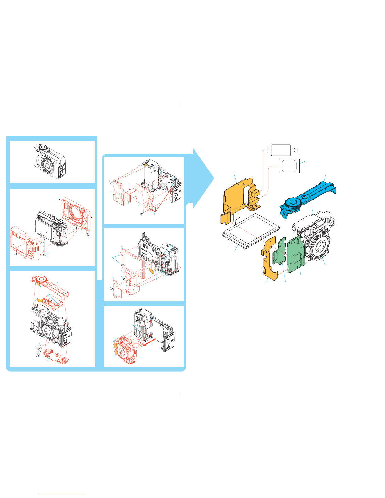
2. DISASSEMBLY
2-1. Flow Chart ······································································· 2-1
2-2. SY-102 Board Service Position ·······································2-3
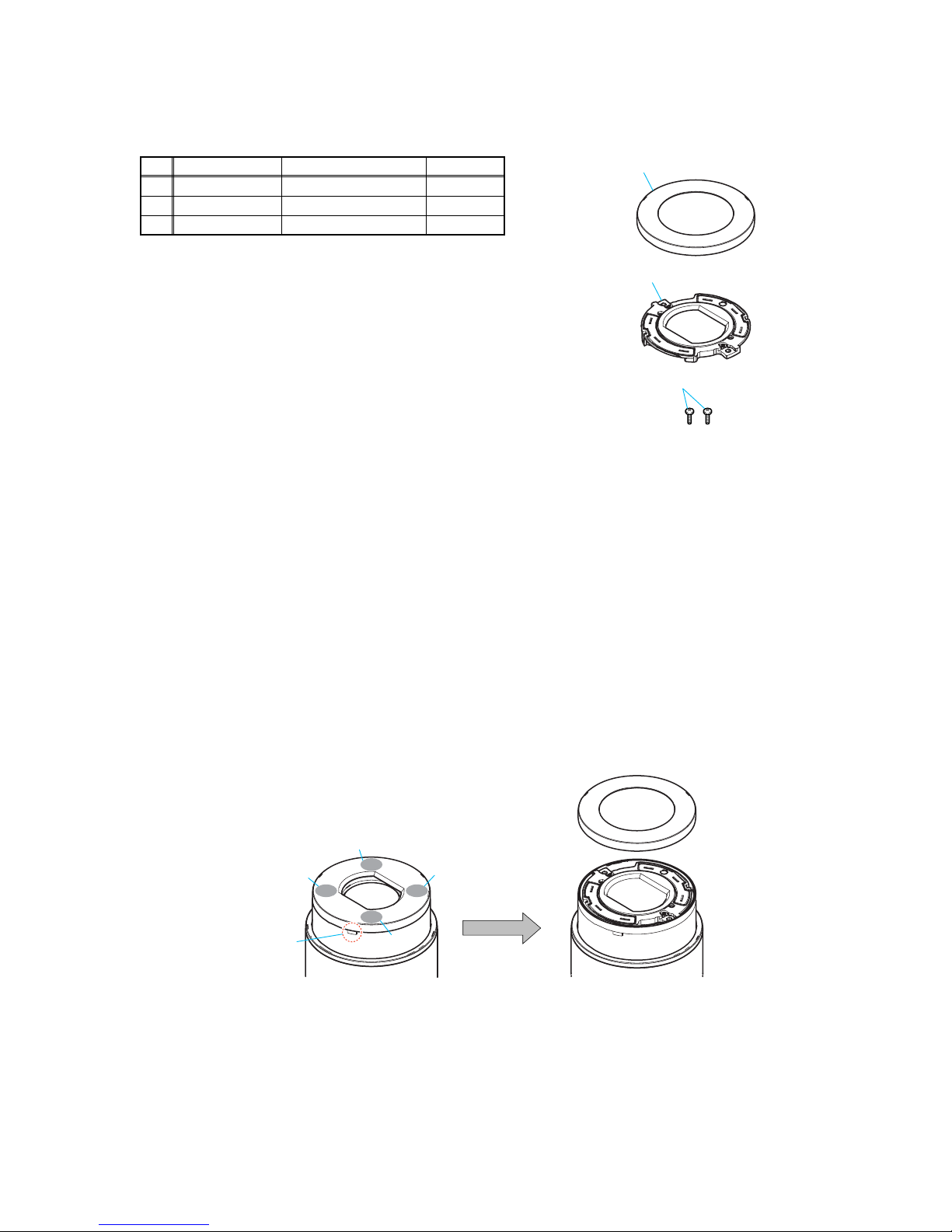
2-3. Exchange Method of Barrier Assy ··································2-5
2-3-1.Peel Off Old Ornamental Ring A ····································2-5
2-3-2.Remove Old Barrier Assy················································2-6
2-3-3.Install New Barrier Assy ·················································2-6
2-3-4.Adhere the Ornamental Ring A ·······································2-7
2-4. Circuit Boards Location ·················································· 2-8
3. BLOCK DIAGRAMS
3-1. Overall Block Diagram (1/2)···········································3-1
3-2. Overall Block Diagram (2/2)···········································3-3
3-3. Power Block Diagram (1/2)·············································3-5
3-4. Power Block Diagram (2/2)·············································3-7
4. PRINTED WIRING BOARDS AND
SCHEMATIC DIAGRAMS
4-1. Frame Schematic Diagram ··············································4-1
4-2. Schematic Diagrams························································4-5
CD-507 FLEXIBLE (CCD IMAGER)····························4-7
ST-100 (FLASH DRIVE) ··············································4-29
ST-101 FLEXIBLE
(CHARGING CAPACITOR, FLASH UNIT) ··············· 4-29
US-011 FLEXIBLE (USB CONNECTOR)··················4-31
CONTROL SWITCH BLOCK ·····································4-32
4-3. Printed Wiring Boards ···················································4-35
CD-507 FLEXIBLE ······················································4-37
ST-100 ···········································································4-49
ST-101 FLEXIBLE ······················································· 4-50
US-011 FLEXIBLE·······················································4-51
4-4. Mounted Parts Location ················································ 4-53
5. REPAIR PARTS LIST
5-1. Exploded Views·······························································5-2
5-1-1.Cabinet Block Section ·····················································5-2
5-1-2.Main Block Section ·························································5-3
5-1-3.Lens Block Section··························································5-4
5-1-4.Side Frame Block Section ···············································5-5
5-2. Electrical Parts List ·························································5-6
Section Title Page
1-1
SECTION 1
SERVICE NOTE
DSC-W1/W12
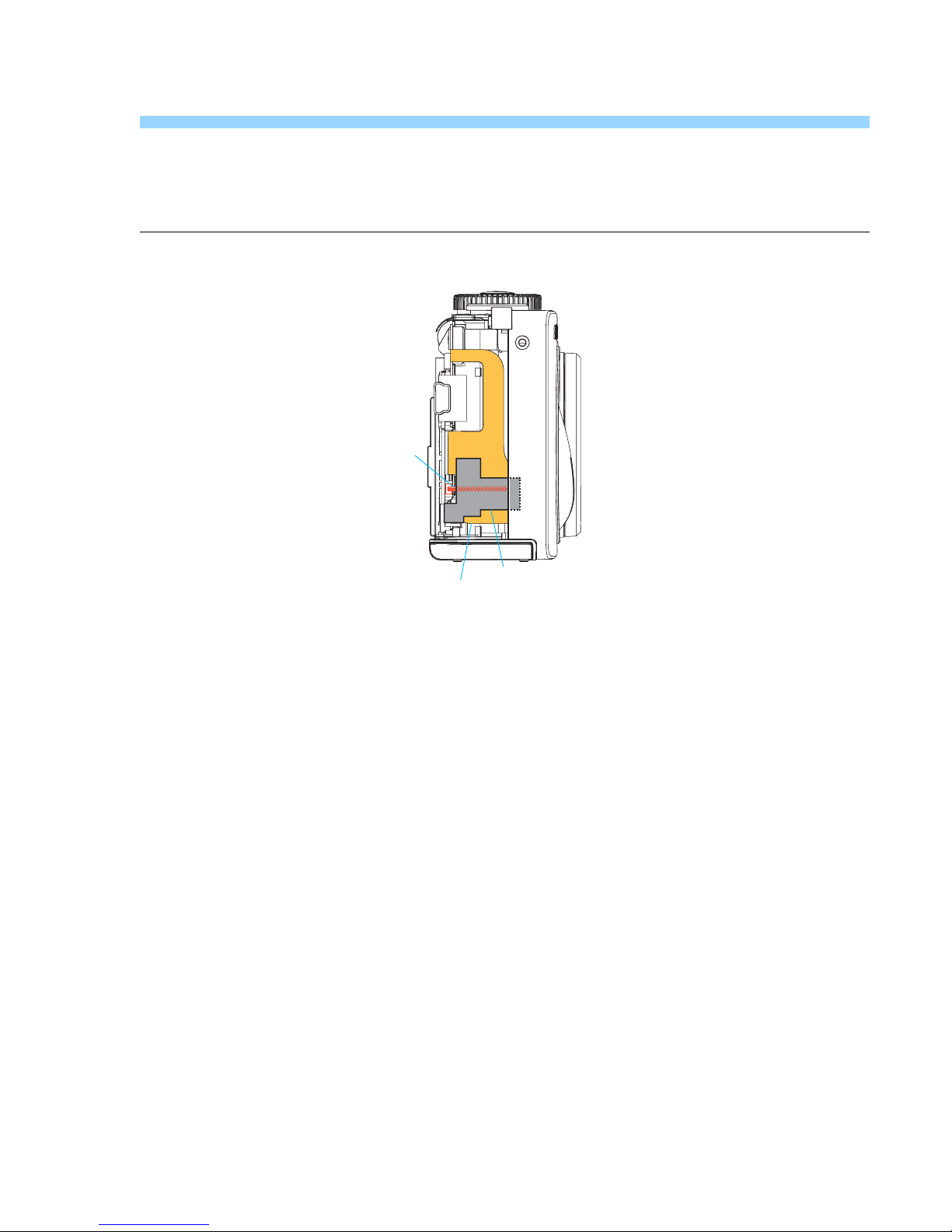
1-2. DISCHARGING OF THE ST-101
FLEXIBLE BOARD’S CHARGING
CAPACITORS (C102 AND C103)
The charging capacitors (C102 and C103) of the ST-101 flexible
board are charged up to the maximum 300 V potential.
There is a danger of electric shock by this high voltage when the
capacitor is handled by hand. The electric shock is caused by the
charged voltage which is kept without discharging when the main
power of the unit is simply turned off. Therefore, the remaining
voltage must be discharged as described below.
Preparing the Short Jig
To preparing the short jig, a small clip is attached to each end of a
resistor of 1 kΩ /1 W (1-215-869-11).
Wrap insulating tape fully around the leads of the resistor to prevent
electrical shock.
1 kΩ/1 W
Wrap insulating tape.
Discharging the Capacitor
Short-circuit between the positive and the negative terminals of
charged capacitor with the short jig about 10 seconds.
1-1. NOTE FOR REPAIR
Make sure that the flat cable and flexible board are not cracked of
bent at the terminal.
Do not insert the cable insufficiently nor crookedly.
Cut and remove the part of gilt
which comes off at the point.
(Be careful or some
pieces of gilt may be left inside)
When remove a connector, don’t pull at wire of connector.
It is possible that a wire is snapped.
When installing a connector, don’t press down at wire of connector.
It is possible that a wire is snapped.
R:1 kΩ/1 W
(Part code:
1-215-869-11)
Capacitor
ST-101
ST kemikon sheet
1-2E
DSC-W1/W12
Display Code
1-4. DESCRIPTION ON SELF-DIAGNOSIS DISPLAY
Self-diagnosis display
• C: ss: ss
You can reverse the camera
malfunction yourself. (However,
contact your Sony dealer or local
authorized Sony service facility
when you cannot recover from the
camera malfunction.)
• E: ss: ss
Contact your Sony dealer or local
authorized Sony service facility.
1-3. NOTE IN LENS FRAME INSTALLATION
When tightening a screw, have both sides of the lens block assembly so as not for the load to depend.
C:32:ss
C:13:ss
Countermeasure
Turn the power off and on again.
Format the “Memory stick”.
Insert a new “Memory Stick”.
Cause
Trouble with hardware.
Unformatted memory stick is inserted.
Memory stick is broken.
Caution Display During Error
SYSTEM ERROR
FORMAT ERROR
MEMORY STICK ERROR
E:61:ss
E:91:ss
Checking of lens drive circuit.
When failed in the focus and zoom
initialization.
Abnormality when flash is being
charged.
Checking of flash unit or replacement
of flash unit.
—
Insert batteries correctly. Batteries are not inserted correctly.
Batteries were installed or removed when
using the AC adaptor.
Turn the power off and on again.
E:92:ss
M1.4 × 4
Lens frame
Lens block assembly
DSC-W1/W12
2-1 2-2
2-1. FLOW CHART
The following flow chart shows the disassembly procedure.
SECTION 2
DISASSEMBLY
HELP
HELP
Note: When you exchange rings, be sure
to follow the procedure carried on
"2-3. Exchange Method of Barrier
Assy" (2-5 page).
HELP
1 Open two connectors (CN201, 701)
2 Claw
x2
3 Lens block
4 CD-507: CN701
5 Lens block flexible: CN201
1
3
4
5
5
0
qa
7
8
2
6
9
1
2
4
5
6
8
9
7
3
0
1 Lock ace screw (M1.7)
x4
2 Claw
3 Rear cabinet
4 Side cover
5 Sheet (S)
6 Mic harness: CN102
7 Lock ace screw (M1.7)
x2
8 Front cabinet
1 BT terminal flexible: CN001
2 Tapping screw (M1.7)
x2
3 SY-102
4 MS-205 flexible: CN704
5 Lock ace screw (M1.7)
x2
6 Tapping screw (M1.7)
x2
7 Boss
8 DC and A/V jack
9 Claw
x2
0 MS-205
1 Lock ace screw
(M1.7)
x2
2 SW-422
3 US-011 flexible: CN101
4 Lock ace screw
(M1.7)
x1
5 Claw
x4
6 US-011
7 Claw
x2
8 Claw
x2
9 LCD block
0 LCD flexible: CN801
qa Back light
flexible: CN802
1 Claw
x1
2 Claw
x1
3 Control SW block
4 Control SW block flexible: CN702
5 ST-101 flexible: CN601
6 Claw
x2
7 Strobo block
8 Tapping screw (M1.7)
x1
9 DC ground plate (B)
0 Claw
x2
qa Claw
x1
qs Bottom cabinet
3
qs
3
8
3
7
2
1
1
1
8
1
2
2
9
0
1
2
4
5
6
qa
0
Note: High-voltage cautions
Discharging the Capacitor
Short-circuit between the two
points with the short jig about 10
seconds.
4
5
6
7
R:1 kΩ/1 W
(Part code:
1-215-869-11)
Capacitor
ST-101
ST kemikon sheet
4
5
9
1 Ornamental ring (A)
2 Tapping screw (M1.2)
x2
3 Barrier assy
1
2
3
DSC-W1/W12
2-3 2-4
2-2. SY-102 BOARD SERVICE POSITION
Lens block
LCD block
Stroboscope block
MS-205 flexible board
US-011 flexible board
SY-102 board
Control switch block
SW-422 board
Color monitor
AC power
adaptor
AC IN
3
8
2
1
1
1
4
5
6
7
3
1
2
2
4
5
1
3
4
5
5
0
qa
7
8
2
6
9
1
2
4
5
6
8
9
7
3
9
qs
0
3
7
8
9
0
1
2
4
5
6
qa
0
2-5
DSC-W1/W12
2-3. EXCHANGE METHOD OF BARRIER ASSY
Service parts
Part Number Part Name Quantity
1 3-091-427-01 Ring (A), Ornamental 1
2 X-3954-476-1 Barrier Assy 1
3 3-086-156-31 Tapping screw (P2) 2
Tools used
Torque driver
Soldering iron
Weight about 60g
Adhesive (Super X) (Note)
Note: Use adhesive (Super X) or an equivalent article.
Don’t use what becomes white after drying like a quick-drying glue.
2-3-1. PEEL OFF OLD ORNAMENTAL RING A
The Ornamental Ring A has adhered to the Barrier Assy strongly and accordingly, use a soldering iron to weaken the adhesive force.
Heat four circled portions with the soldering iron.
Heating temperature is about 300ºC.
Beware of a burn since the entire Ornamental Ring becomes hot.
* As the adhesive force of Ornamental Ring A is considerably large, the forced peeling will damage the group-1 frame.
Insert the tip of tweezers, etc. into a notch of the group-1 frame and prize the ring.
* Take extreme care so as not to damage the coated surface of the group-1 frame.
In case of difficult peeling, heat the ring again with the soldering iron.
If this re-heating failed, it may be advisable that the ring be peeled while heating the portions 1 → 2 → 3 → 4 in the under figure one
by one sequentially.
* Discard the removed Ornamental Ring A.
1
2
3
1
Tip
3
4
2
2-6
DSC-W1/W12
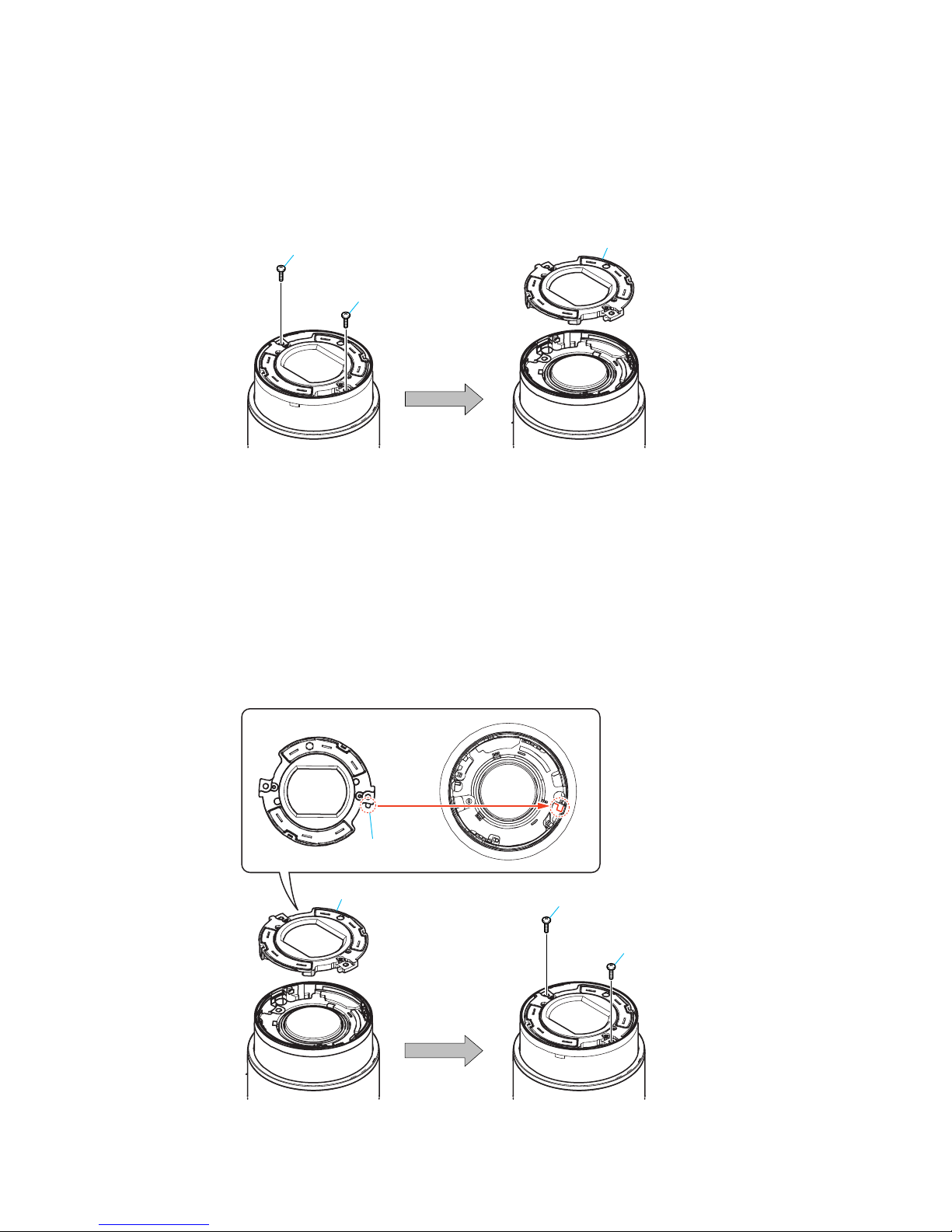
2-3-2. REMOVE OLD BARRIER ASSY
1 Remove two screws.
* Discard the removed screws.
2 Remove the Barrier Assy.
* Discard the removed Barrier Assy.
* After removing the Barrier Assy, if the “G1 Dust-Proof Ring” was removed, it must be returned to the home position.
In returning the ring, adjust the location of a projection to the lens direction.
This is an important part to prevent the dust and light from coming in.
* After removing the Barrier Assy, take extreme care not to drop dust or foreign substances in the lens barrel.
2-3-3. INSTALL NEW BARRIER ASSY
1 Install new Barrier Assy by paying attention to the projection of the Barrier Assy in relation to the position shown in the under figure.
2 Tighten two screws.
* Tightening torque = 0.5 kgf
1
1
2
Projection
2
2
1
2-7
DSC-W1/W12
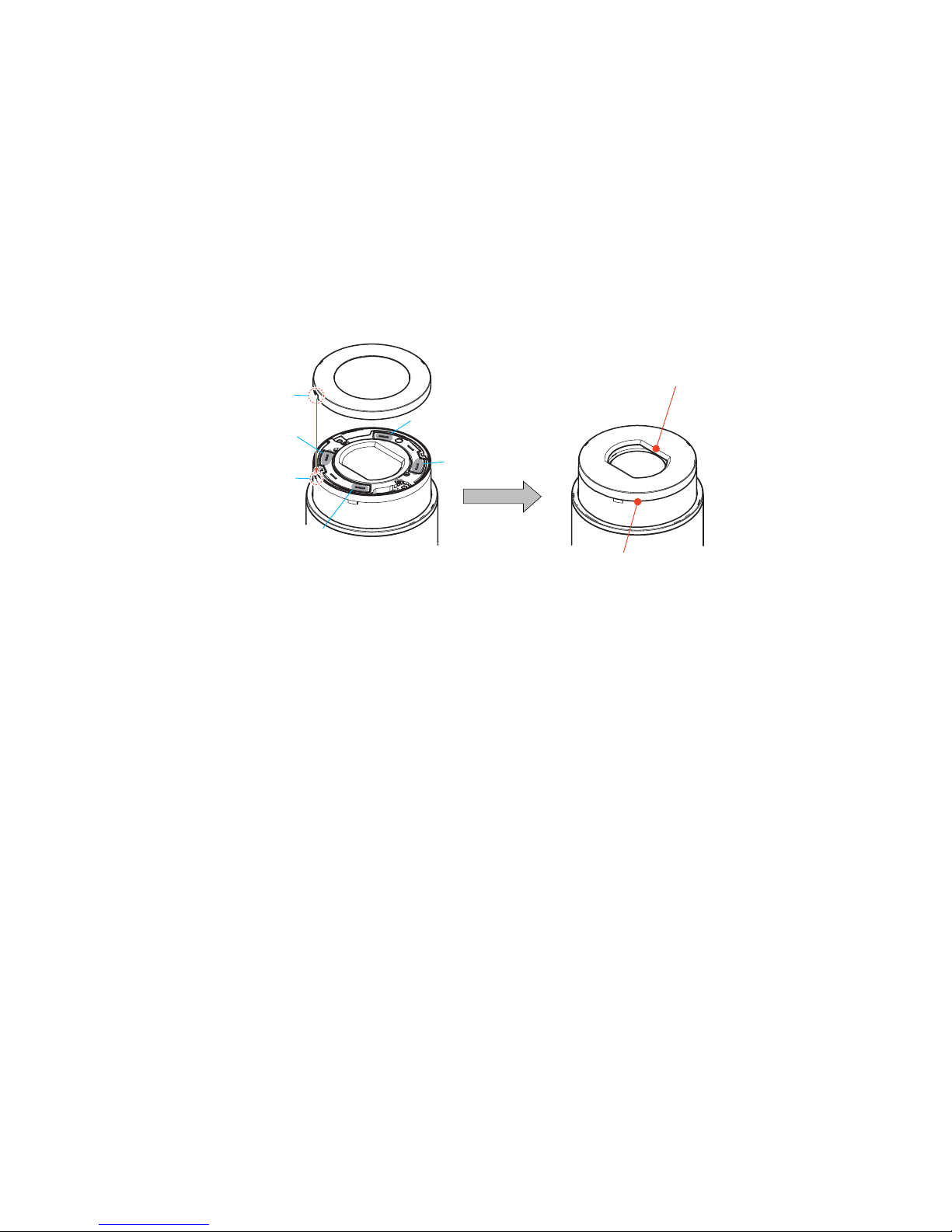
2-3-4. ADHERE THE ORNAMENTAL RING A
Apply an adhesive to four recesses on the top surface of the Barrier Assy.
* Do not apply too much adhesive. (Make quantity of adhesives into the quantity in which a groove hides.)
Meeting a “notch” of the Ornamental Ring A with a “projection” of the group-1 frame, push the Ornamental Ring A into the group-1 frame.
* The projection of the spring for preventing static electricity must be tilted.
Put the 60g weight on the Ornamental Ring A so that the Ornamental Ring A does not float up until the adhesive hardens.
Note: Be careful not to give a shock.
* After the weight was put, no gap must be present in full circumference between Ornamental Ring A and group-1 frame.
A gap, if present, causes the crackle sound NG.
* The weight must push in the Ornamental Ring A only.
If the weight is put on the mold part of the Barrier Assy, the Ornamental Ring A will float up.
Completion after 30 minutes.
Notch
Adhesive
Adhesive
Adhesive
Do not put the weight on a black mold part.
Not gap in full circumference.
Adhesive
Projection
2-8E
DSC-W1/W12
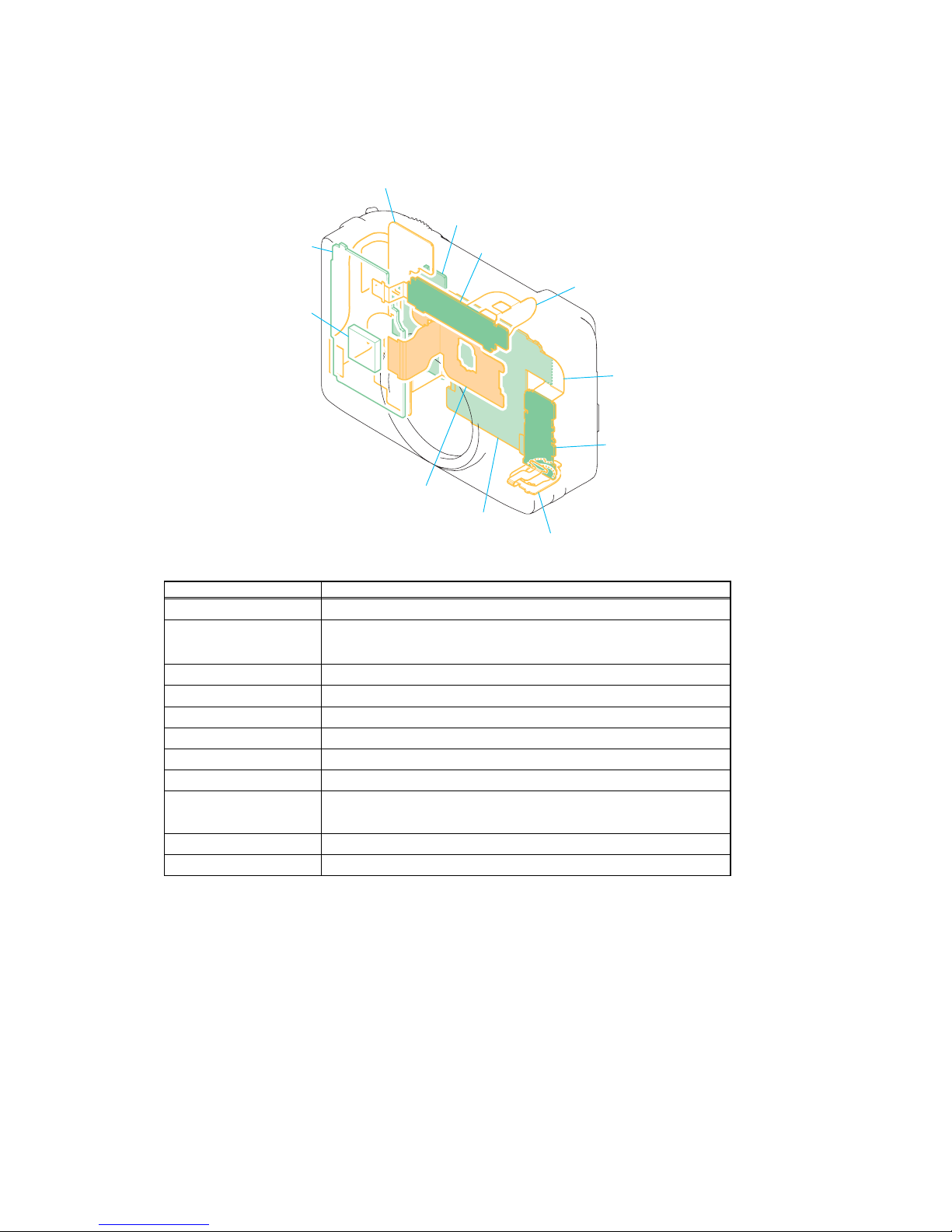
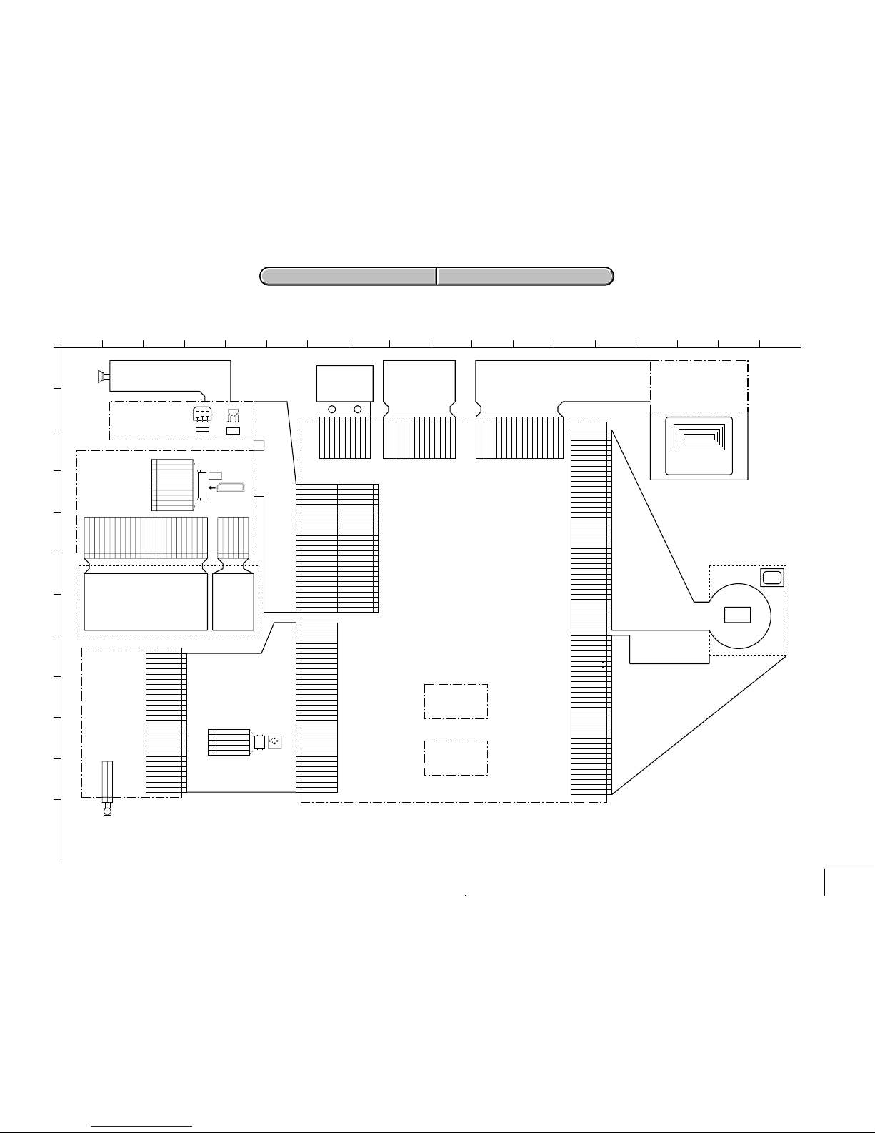
2-4. CIRCUIT BOARDS LOCATION
CD-507 flexible
US-011 flexible
SY-102
(including CH-146)
ST-101 flexible
ST-100
SW-422
CH-146
(included in SY-102)
JK-263
MS-205 flexible
MS-204
SP-045 flexible
Board Name Function
CD-507 flexible CCD IMAGER
CH-146 CCD SIGNAL PROCESS
(included in SY-102)
JK-263 JACK
MS-204 LCD DRIVE, MS CONNECTOR
MS-205 flexible CONNECTOR
SP-045 flexible SPEAKER
ST-100 FLASH DRIVE
ST-101 flexible CHARGING CAPACITOR, FLASH UNIT
SY-102 CAMERA MODULE, CAMERA DSP, LENS DRIVE,
(Including CH-146) SH DSP, FRONT CONTROL, DC/DC CONVERTER
SW-422 AUDIO, CONTROL SWITCH
US-011 flexible USB CONNECTOR
DSC-W1/W12
HELP
US-011 flexible board
Mic harness
Front side
Sheet (S)
HELP
Sheet attachment positions and procedures of processing the flexible boards/harnesses are shown.

DSC-W1/W12
Link
Link
3. BLOCK DIAGRAMS
OVERALL BLOCK DIAGRAM (2/2) POWER BLOCK DIAGRAM (2/2)
POWER BLOCK DIAGRAM (1/2)OVERALL BLOCK DIAGRAM (1/2)
OVERALL BLOCK DIAGRAM (2/2) POWER BLOCK DIAGRAM (2/2)
POWER BLOCK DIAGRAM (1/2)OVERALL BLOCK DIAGRAM (1/2)
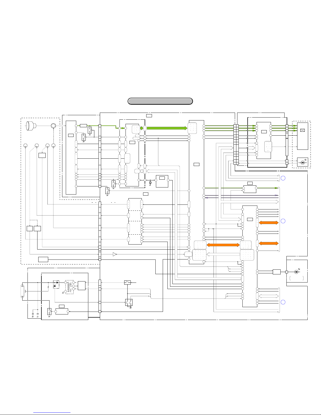
DSC-W1/W12
3. BLOCK DIAGRAMS
3. BLOCK DIAGRAMS
LENS
IRIS
(METER)
CCD
IMAGER
IC101
CD-507 FLEXIBLE BOARD (1/2)
SY-102 BOARD (1/2)
17
19
86
133
CAMERA
MODULE
(1/6)
AU AIN
V OUT
PANEL R
HR EN2,
HR DIR2A,
HR DIR2B
STRB CHRG
XSTRB FULL
ST UNREG
48
MCKTG
XFE CS, XTG CS
47
TG CLK
CP101
22
ı
35
40
ı
42
23
25
24
A12
B12
C23
B13
D13
C13
AC8
AC22
33
42
51
IRIS
MOTOR
M
LENS BLOCK
XFC RST SENS
XSYS RST
SYS V
1
OVERALL (2/2)
(PAGE 3-3)
2
OVERALL (2/2)
(PAGE 3-3)
USBPHY D±
FR SI, FR SO, XFR SCK
P4
C6
D7
F1
G1
AC12
AC15
Y11 AB11 Y10
AA11 AB10
Y9
AB9 AA10 AA9
Y8
AB8 AA8
AB7
AA7
U20 V21 V23 U22
V20
V22 W20 Y20
W22
Y23 W21 Y22
Y21
AA22 AA21 AB22
J21 L22 L20 L23 K21
L21
M21 M23 M20 M22
N21
N22 N20 P20 P21
P23
R21 P22 T21 R23
R20
R22 T20 T23 U21
L21 L23 M24 K23
H22
J21 J22 F24
K21
H21 M23 K22
G21
L24 F23 E23
V22 V21 V23 R22 W22
U22
W21 T22 R23 N21
P22
P21 P23 R21 M22
T21
P24 U21 U23 N22
U24
N23 T24 M21 T23
B16
B15
D16
IC304
51
IC501
CN701
(1/2)
LENS TEMP
IC201
ZOOM
MOTOR
M
ZOOMFGZOOM
SENSOR
FOCUS
MOTOR
M
FOCUS
SENSOR
J1
K1
L1
M1
X301
54MHz
A : VIDEO SIGNAL
A : AUDIO SIGNAL
A : VIDEO/AUDIO SIGNAL
4
10
7
34
30
ı
28
26
ı
23
16
C1
D2
G5
H6
G4
H4
MC MSDIO,
MC MSBS,
MC MSCLK
BACKLIGHT
COLOR
LCD
MONITOR
D11
L7
L8
J11
L6
A5
B4
A4
A11
B11
C11
VR
VG
VB
COM
BL H
5
3
23
24
2
6
ı
8
11
ı
14
19
ı
22
4
CN801
3
CN802
D901
LCD901
RGT, HCK1, HCK2,
HST, PCG, XSTBY,
DWN, EN, VST,
VCK, REF, VP
HDO
PANEL V
LCD DRIVE
IC801
B1
A2
SYS V
MC D0 – D15
MC A1 – A25
Q602, 603
D8
J23
J22
AA12
D14
A17
C18
D21
AD16
K2
A7
H1
AA8
M
SHUTTER
MOTOR
LENS TEMP
SENSOR
24
ı
27
17
ı
20
5
ı
8
1
ı
4
29
21
VER EXT CLK
F4
F3
U3
T2
T3
U2
T4
AA19
AB20
E7
D7
MSHUT EN
MSHUT DIR
F8
F7
IRIS S EN
IRIS S IN
G2
G1
IRIS M EN
IRIS M IN
XZM DC BR
G3
H2
B1
FOCUS
MOTOR
DRIVER
ZOOM
MOTOR
DRIVER
IRIS
MOTOR
DRIVER
SHUTTER
MOTOR
DRIVER
H8
MSHUT REF
HR EN0,
HR DIR0A
IRIS M±, S±
Z DC MOTOR ±
F MOTOR A, A, B, B
SHUTTER ±
CN201
BUFFER
Q102
IC301
XTG CS
XFE CS
CAM F
XSYS RST
MC XCS IC 301REG
MC XCS IC 301SDRAM
XSYS RST
XPANEL TG CS
XPANEL TG CS
VIDEO AMP ON
P1
MC CKIO
A2
A6
G2
AC12
AA9
AC16
AC15
AD19
AB11
LENS TEMP
VER EXT CLK
PANEL B
PANEL G
D1
E1
E11
F11
MS-205 FLEXIBLE BOARD (1/3)
MS-204 BOARD (1/3)
E1 F1 G2
H2 H1 J2
J1 K1 K3
L3
H11
K11
L10
PANEL UNIT
31
XZM RST SENS1
ZM DC FG A, B
F PI SENS OUT
Z PI SENS OUT
Z BOX1 PI SENS OUT,
Z BOX2 PI SENS OUT
IRIS M±, S±
ZOOM DC ±
FOCUS A, A, B, B
SHUTTER±
AU AOUT
A6
B5
A4
B4
1
3
5
6
36
35
33
32
11
7
26
27
31
7
11
30
31
19
135
37
48
9
6
12
15
19
10
13
17
20
113 109
112 115
125 119
118 121
6
37
5
2
4
20
19
21
36
1
3
7
8
10
11
9
12
ı
18
CAMERA DSP,
SDRAM
(KWF BOARD)
(2/6)
CA AD00 – CA AD13
AB6
46
CAM SO, XCAM SCK, XCAM RST
CAM SO, XCAM SCK, XCAM RST
CAM SO, XCAM SCK, XCAM RST
CLOCK
GENERATOR
(2/6)
LENS DRIVE
(3/6)
MSHUT REF
AA19
XZM DC BR
ST-100 BOARD
ST-101 FLEXIBLE BOARD
CN601
05
Q003
FLASH
UNIT
Q105
Q103
4
1
FLASH
CONTROL
4
2
IC001
VIDEO AMP
(2/6)
24
1
IC302
12
ı
17
Q604
XE_H
CL025 – 030,
044, 045
CL038
CL039
CL041
CL801–803
CL804,
807, 808
CL811,
813, 814
CL001,
003 – 007,
042
TRIG 300V
XE_L
CL022
CL021, 043
+ +
C102, 103
CHARGING
CAPACITOR
D005
2
5 4
1
3
T001
STB FULL
ST UNREG
STB ON
XSTB FULL
STB ON
STRB CHRG
XSTRB FULL
STRB ON
AD14
AB7
MELODY
F1
PRELAMP AF CONT
H23
SELF TIMER LED
C22
XACCESS LED
L22
TALLY LED
AB5
XAE LOCK ON
AD20
XAE LOCK LED ON
AB13
XSHTR ON
AD11
FR INT
D11
XCS MC
MELODY ENV
D22
AA18
AU SEN
XAU LINE MUTE
BL LEV
LED A
LED K
BL H
OVERALL (2/2)
(PAGE 3-4)
3
C1
G10
13
11
9
CN704
(1/3)
CN001
(1/3)
14
BL L
1
BL L
27
B5
BL LEV
MC CAM,
SH DSP,
FLASH
(4/6)
CAM F
CAM F
Y7
45
CA HD
4
8
ı
10
12
ı
15
CCD OUT
POWER SAVE
20
V2, V4, V5A, V5B,
V6, V7A, V7B, V8
RG, H1B, H2B
V1A, V1B,
V3A, V3B
VHOLD
VST
21
VSUB
H1A, H2A
27
Q105
Q701
VSUB CONT
38
39
99
84
134 136
2 4
6 9 12 15
18 21 24
27 30 32
3
123
126
–
129
49
105
132
124
B7
B8
C7
C8
B3
A2
K4
J3
G4 J2 Y4
G3 H4 W4
N3
K3
M4
SYS SO, XSYS SCK
SYS SI, SYS SO, XSYS SCK
SYS SI, SYS SO, XSYS SCK
CH-146 BOARD
CCD SIGNAL
PROCESSOR,
TIMING
GENERATOR
IC101
66
101 120
Q205
27MHz
3
TRANS
DRIVE
Q001, 002
XSTRB PWR SAVE
XSTRB PWR SAVE
XSTRB PWR SAVE
19
17
2
8
6
21
10
4
13
11
9
14
CL810
CL812
CL817
CL815
CL816
CL820
CL821
CL819
27
19
17
2
8
6
21
10
4
CD-507 FLEXIBLE
BOARD (2/2)
CN701
(2/2)
39
Q702
LED
DRIVE
D101
SELF TIMER/
AF ILLUMINATOR
XLED
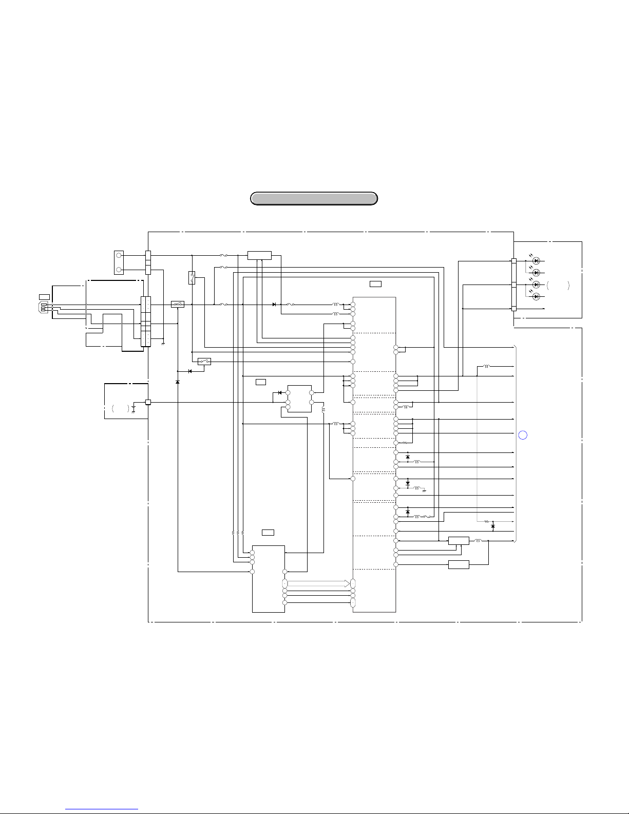
3-1. OVERALL BLOCK DIAGRAM (1/2)
3-1 3-2
( ) : Number in parenthesis ( ) indicates the division number of schematic diagram where the component is located.
SECTION 3
BLOCK DIAGRAMS
DSC-W1/W12
3. BLOCK DIAGRAMS
3. BLOCK DIAGRAMS
A : VIDEO SIGNAL
A : AUDIO SIGNAL
A : VIDEO/AUDIO SIGNAL
USB JACK IN
SY-102 BOARD (2/2)
SW-422 BOARD
(1/2)
US-011 FLEXIBLE BOARD (1/2)
SW-422 BOARD (2/2)
US-011 FLEXIBLE BOARD (2/2)
AUDIO AMP
IC151
H7
F1
A7
05
MIC901
V OUT
AU AIN
AU AOUT
AU SEN
MELODY ENV
TALLY LED
XAE LOCK LED ON
XTALLY LED
XRSTX XRSTX
XAE LOCK LED
XCHARGE LED
XCHARGE/XSTRB LED
XCHARGE/XSTRB LED
MELODY
H6
H4
SP901
SPEAKER
V OUT V OUT
MIC IN
CN101
(2/3)
CN102
1
OVERALL (1/2)
(PAGE 3-2)
MODE
DIAL
S001
(SHUTTER)
POWER
CONTROL SWITCH BLOCK
S002
8
XPWR ON
MODE DIAL0, 1 MODE DIAL0, 1
B8
B2
J8
J9
D1
D2
E1
6
XPWR LED
D001
(POWER)
S901
USBPHY D± USBPHY D±
FR INT
XCS MC
XAE LOCK ON
IC401
D9
E2
DC/DC
CONTROL,
RESET
(6/6)
IC001
DDCON SO, DDCON SCK
C1
D3
L8
K8
D 1.2V ACV UNREG
PANEL 8.5V
BACK UP VCC
EVER 3.0V
A 3.1V
D 2.8V
CAM 15.5V
A 2.8V
CAM –7.5V/–8.0V
CAM 3.3V
ST 5V
M 5V
A7
H2
C7
D7
SYS SO, XSYS SCK SYS SO, XSYS SCK
H2
H3
CN702
9
USB JACK IN
AV JACK IN
2
OVERALL (1/2)
(PAGE 3-2)
Q402
Q502
MODULATOR
SYS V
FR SI, FR SO, XFR SCK
B9
XSYS RST
B3
J5
J4
D7
X401
32.768kHz
RESET
S201 – 208
1
2
KEY AD0, 1
KEY AD0, 1
KEY AD2
KEY AD0, 1
KEY AD2
CN101
(3/3)
CN703
(3/3)
A2
A4
A3
C8
XMS IN
Q401
B6
AV OUT
(MONO)
2
3
(USB)
CN001
J101
MS-205 FLEXIBLE BOARD (2/3) SP-045 FLEXIBLE
BOARD
JK-263 BOARD
(1/2)
42
6
ı
10
1
ı
5
3
2
4
1
XSHTR ON
XAE LOCK ON
XPWR ON
XPOWER LED ON
CHG SW
FAST CHARGE
XRSTX
Q010
Q001
BATT/XEXT
CN704 (3/3) CN001 (3/3)
CN001
29
ACV UNREG1
+
−
JK-263 BOARD
(2/2)
MS-205 FLEXIBLE BOARD
(3/3)
MS-204 BOARD
(3/3)
DC IN
J102
BT901
BATTERY
TERMINAL
BATT UNREG
BATT GND
GND
J2
J3
VCC
ACV UNREG
ST UNREG
BATT UNREG
C1
XAU LINE MUTE
G4
XSHTR ON
B1
FRONT
CONTROLLER
(5/6)
B1
G2
OVERALL (1/2)
(PAGE 3-2)
3
LED K
BL LEV
E4
E3
A9
BATT IN
H1
XCS DDCON
K7
E8
SYS DD ON
G1
LED A
BATT/XEXT
Q503
LED
DRIVE
PLL
LOOP
FILTER
Q501
LED
DRIVE
D002
SELF TIMER/
RECORDING
D003
(AE/AF LOCK)
D004
(FLASH CHARGE)
21
2
10
11
1
7
15
23
24
CN703
(2/3)
28
30
31
CN101
(1/3)
12
14
16
10
19
5
7
15
22
CN703
(1/3)
3
AU AIN
26
XAU LINE MUTE
23
AU SEN
AU AOUT
SP±
21
BEEP
20
AU OUT
18
D±
XACCESS LED
XACCESS LED
MC MSDIO, MC MSBS, MC MSCLK MC MSDIO, MC MSBS, MC MSCLK
MEMORY
STICK
4
2
8
6
MC MSDIO, MC MSBS, MC MSSCLK
XMS IN
MS-204 BOARD
(2/3)
CN901
2
33
9
10
BT001
LITHIUM
BATTERY
J6
H6
FUNCTION
KEY
S002
W
S001
T
(ZOOM)
G6
VL 3V
VL 3V
CL101–104
CL105–108
CL109
CL927
LND008, 009CL144, 145
CL924CL919 CL112
AU OUT
CL925
CL916
CL113
CL118
AV JACK IN
CL923 CL111
SP±SP± LND006, 007
CL922
CL901
44
46
48
50
43
45
47
49
42
29
44
46
48
50
43
45
47
49
CN704 (2/3) CN001 (2/3)
16
33
37
30
28
35
16
33
37
30
28
35
41 41
AU OUT
V OUT
SP±
AU OUT
CL920
CL917
34 34
AV JACK IN
CL918
XMS IN
CL907
CL905,
909, 911
38
38
40 40
Q902
LED
DRIVE
D105
(MS ACCESS)
INITIAL
RESET,
BACK UP VCC
(6/6)
IC002
4 5
3
2
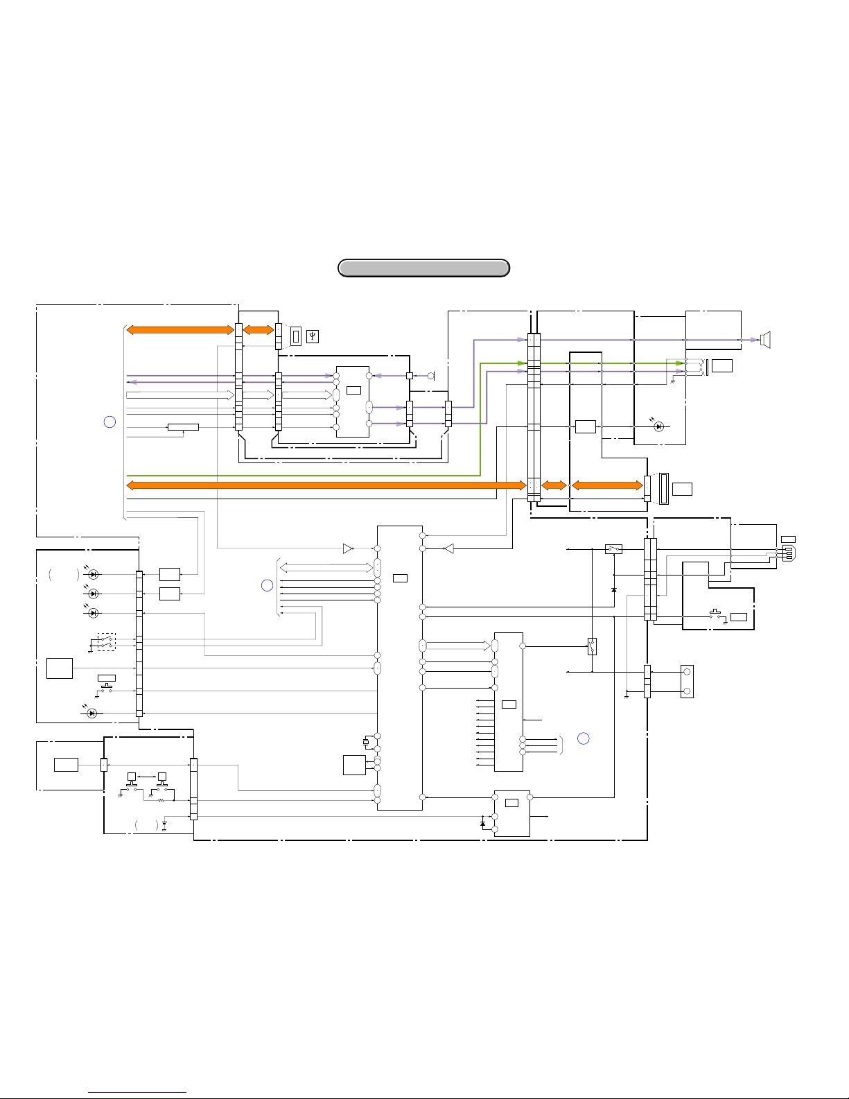
3-3 3-4
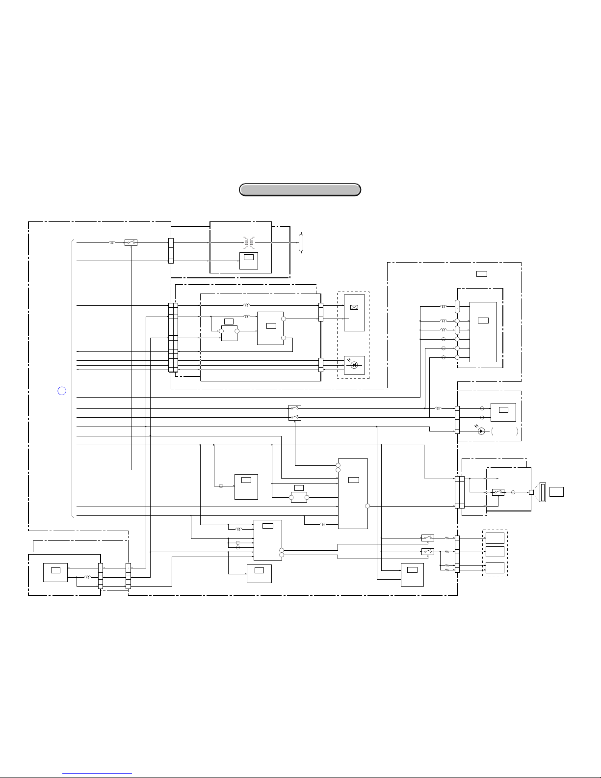
3-2. OVERALL BLOCK DIAGRAM (2/2)
( ) : Number in parenthesis ( ) indicates the division number of schematic diagram where the component is located.
DSC-W1/W12
3. BLOCK DIAGRAMS
3. BLOCK DIAGRAMS
POWER 2
(PAGE 3-7)
A
05
SY-102 BOARD (1/2)
CONTROL SWITCH BLOCK
VCH1A
D 2.8V
VCH2
VCC1A
G11
ODP SW
C9
CHG SW
E4
VDCIN
D1
TLD
H6
CPSW
E8
OUT8B
E9
VCC8
B11
OUT8A
D9
L10
VCH1B
K9
VCH1C (FB4)
L9
VCH7
K3
VOS73
L3
VOS72
K4
E11
OUT2
F10
IC001
DC/DC CONTROL
(6/6)
VCC2
F9
VCH8A
C10
VCH8B
C11
VLDO1
A11
D 1.2V
M 5V
ST 5V
A 2.8V
VCC1C
G9
VCC1B
G10
BATT
D4
MARK
E5
OUT3C
J2
OUT3B
K1
VCH3A (FB3)
J1
VCH3B
H4
VCH3C (FB6)
H3
VCH3S
H2
VCC GD
H1
D008
D012
D001, 002
BATT UNREG
D 1.2V
ACV UNREG
D 1.2V
ACV UNREG
L001, 002
L014
L015
L012
L003
VCH4
J6
OUT4
K6
CAM 15.5V
CAM 3.3V
VLDO4
C8
A 3.1V
L007
D010
BL THH
EVER 3.0V
IC401
FRONT CONTROLLER
(5/6)
ST UNREG
D 2.8V
G8
A7
ACV SENS
F8 DD CON SENS
BATT/XEXT
H8 BATT SENS
F003
F002
F001
F005
14
13
CN702
BACK UP VCC
6
ı
10
1
ı
5
OUT3A
J3
VCC5
DIN
CLK
SYSDDON
USB PWR ON
LD
FCHG
K5
VCC7
J4
Q010
Q003, 011
Q001
Q002
CN001
+
−
BT901
BATTERY
TERMINAL
BATT UNREG
BATT GND
DC CONTROL
VCH5
J5
OUT5
L5
CAM –7.5V/–8.0V
VLDO5
B8
PANEL 8.5V
LED A
L011
D009
VCH6
G1
OUT6
F1
LED K
BL LEV
ICH6
G2
REF6
B1
D006
D004
L006
L004
F004
DDCON SO,
DDCON SCK
C1
D3
L8
K8
H2
C7
D7
FAST CHARGE
E3
A9
BATT IN
H1
XCS DDCON
K7
E8
SYS DD ON
D001
(POWER)
D 2.8V
12
D 2.8V
42
CN704
(1/3)
CN001
(1/3)
ACV UNREG1
JK-263 BOARD
MS-205 FLEXIBLE BOARD
(1/3)
MS-204 BOARD
(1/3)
DC IN
J102
GND
BATT/XEXT
CL101–104
CL105–108
CL109
CL927 CL922
44
46
48
50
43
45
47
49
42
44
46
48
50
43
45
47
49
BT001
LITHIUM
BATTERY
D005
CN703
(1/2)
US-011 FLEXIBLE
BOARD (1/2)
33
VL 3V
VL 3V
Q007, 008
SWITCHING
Q009
DC CONTROL
L013
D002
SELF TIMER/
RECORDING
D003
(AE/AF LOCK)
D004
(FLASH CHARGE)
INITIAL RESET,
BACK UP VCC
(6/6)
IC002
4
7VIN
6VOUT
CS
3
VBAT
2
VCH
3-5 3-6
3-3. POWER BLOCK DIAGRAM (1/2)
( ) : Number in parenthesis ( ) indicates the division number of schematic diagram where the component is located.
DSC-W1/W12
3. BLOCK DIAGRAMS
3. BLOCK DIAGRAMS
SY-102 BOARD (2/2)
CN201
IC001
11
18
CN801
CN802
F PI SENS Vcc
PU[6]
Q201 (1/2)
REF
BL THH
VDD
Z BOX1 PI
SENS Vcc
05
6
1
ST UNREG
STRB CHRG
CAM DD ON
MS PWR ON
D 2.8V
ST 5V
BL THH
BL LEV BL LEV
PANEL 8.5V
LED A
LED K
BL THH
BL LEV
PANEL 8.5V PANEL 8.5V
PANEL 4.9V
PANEL 2.8V
PANEL 4.9V
PANEL 2.8V
BL H
BL L
MS-205 FLEXIBLE BOARD (2/3)
MS-204 BOARD (2/3)
BL L
3
BL H
REF
BL THH
VDD
BL L
BL H
CAM 15V
CAM –7.5V
13
1
CN701
M 5V
38
L103
L102
L101
L104
FB105
FB102
CCD IMAGER
IC101
CD-507 FLEXIBLE BOARD
POWER 1
(PAGE 3-6)
CAM 15.5V
A 3.1V
D 1.2V
A 3.1V
D 1.2V
CAM 3.3V
CAM –7.5V/–8.0V
M 5V
A 2.8V
M 5V (AU_5V)
A 2.8V
D 2.8V
D 2.8V
D 1.2V
CAM 15.5V
CAM 3.3V
CAM –7.5V/–8.0V
M 5V
A 2.8V
D 2.8V D 2.8V
A
Q901
D 2.8V
Q106, 107
L152
REF
2.8V
REG
L802
L803
CN601
ST UNREG
ST 5V
CL025–030,
044, 045
CL001,
003–007,
042
CL040
AUDIO AMP
IC151
AC20
PU[0]
AD19
SDA(O/D)
AD18
ZOOM
SENSOR
LENS BLOCK
ZOOM
SENSOR
ZOOM
FG
3
CN704
(2/3)
M 5V (PANEL 5V)
1
A 2.8V (PANEL 2.8V)
27
14
12
3
CN001
(2/3)
1
27
14
10 10
12
IC802
H11
EXTDA
G10
5 4
1.8V
REG
(4/6)
IC502
4 1
53
56
51
49
AU 2.8V
A 2.8V
AU 2.8V
A 2.8V
AU 5V
AU 2.8V
A 2.8V
AU 5V
28
9
Z PI SENS Vcc
FOCUS
SENSOR
23
Z BOX2 PI
SENS Vcc
14
25
31
VIDEO AMP
(2/6)
IC302
L301
PI006
V4
VCC
9
XLENZ RST LED
PI007
V3
XZM RST LED
ST-100 BOARD
ST-101 FLEXIBLE
BOARD
T001
FLASH
UNIT
L601
Q602, 603
12
ı
17
2
FLASH
CONTROL
BACKLIGHT
COLOR
LCD
MONITOR
D901
LCD901
LCD DRIVE
IC801
PANEL UNIT
CH-146 BOARD
CCD SIGNAL
PROCESSOR,
TIMING
GENERATOR
CAMERA MODULE
(1/6)
IC101
CP101
FB103
FB101
FB102
FB307
FB303
FB903
FB309
D101
SELF TIMER/
AF ILLUMINATOR
CN704
(3/3)
25
31
CN001
(3/3)
MEMORY
STICK
MS-204 BOARD (3/3)
SW-422 BOARD
US-011 FLEXIBLE BOARD (2/2)
MS-205 FLEXIBLE BOARD (3/3)
CN901
IC501
MC CAM,
SH DSP,
FLASH
(4/6)
D2.8V
A 2.8V
M 5V
D 2.8V
D 2.8V
Q201 (2/2)
D 2.8V
IC304
IC301
CAMERA DSP,
SDRAM
(KWF BOARD)
(2/6)
CLOCK
GENERATOR
(2/6)
IC201
LENS DRIVE
(3/6)
54
55
71
52
57
L502
5 5
CL826–828
CL818,
824, 825
CL902,
928, 929
CL903
CL915,
932
CL809,
822, 823
CL810
CL806
CL804, 807, 808
CL801–803
24
16
13
14
CN703
(2/2)
17
8
5
6
CN101
3-4. POWER BLOCK DIAGRAM (2/2)
3-7 3-8E
( ) : Number in parenthesis ( ) indicates the division number of schematic diagram where the component is located.
DSC-W1/W12
4-2. SCHEMATIC DIAGRAMS 4-3. PRINTED WIRING BOARDS
4-2. SCHEMATIC DIAGRAMS 4-3. PRINTED WIRING BOARDS
F_MOTOR_B
F_MOTOR_A
Z_DC_MOTER_-
Z_DC_MOTER_-
CN102
2P
1
2
J101
J102
5P
CN001
1
89
67
VCC
2
D-
3
D+
4ID
5
GND
10PCN001
123456789
10
31P
CN201
1
2
3
4
5
6
7
8
9
10
11
12
13
14
15
16
17
18
19
20
21
22
23
24
25
26
27
28
29
30
31
17P
CN601
123456789
10111213141516
17
CN702
14P
123456789
1011121314
33P
CN703
1
2
3
4
5
6
7
8
9
10
11
12
13
14
15
16
17
18
19
20
21
22
23
24
25
26
27
28
29
30
31
32
33
50PCN704
1
3
5
7
9
11
13
15
17
19
21
23
25
27
29
31
33
35
37
39
41
43
45
47
49
2
4
6
8
10
12
14
16
18
20
22
24
26
28
30
32
34
36
38
40
42
44
46
48
50
27PCN101
1
2
3
4
5
6
7
8
9
10
11
12
13
14
15
16
17
18
19
20
21
22
23
24
25
26
27
24P
CN801
123456789
101112131415161718192021222324
CN802
6P
12345
6
39P
CN701
1
2
3
4
5
6
7
8
9
10
11
12
13
14
15
16
17
18
19
20
21
22
23
24
25
26
27
28
29
30
31
32
33
34
35
36
37
38
39
CN901 12P
1
2
3
4
5
6
7
8
9
10
1
A
FLASH
CCD
BOARD
N
S
SCLK
SDIO/DATA0
DATA1
DATA2
DATA3
VCC
VSS
INT
MS_BS
VSS
CN001 50P
BATTERY
TERMINAL
BT901
CONTROL
SWITCH
BLOCK
BOARD
CH-146
CP101
KWF
BOARD
IC301
SY-102 BOARD
OVF
CD-507
FLEXIBLE
BOARD
LENS BLOCK
UNIT
ST-100
ST-101
FLEXIBLE
BOARD
COLOR
LCD901
BACK
D901
LIGHT
LCD MONITR
2.5INCH
11
12
MEMORY
STICK
MEMORY STICK
MS-204
BOARD
PANEL UNIT
FLEXIBLE BOARD
MS-205
DC IN AV OUT
(MONO)
BOARD
JK-263
SP901
FLEXIBLE BOARD
SP-045
BOARD
SW-422
FLEXIBLE
BOARD
US-011
MIC
MIC901
(USB)
05
J
B
16
L
564 14
H
38
F
D
E
C
13 15
G
7 1711910 18122
K
I
TEST
RGTBRGPSIG
HCK1
HCK2
WIDE
SOUT
REF
HST
PCG
XSTBY
VSSG
N.C.
VSS
VDD
DWNENVCK
VSTCSCOM
N.C.
BL_L
N.C.
BL_THH
BL_H
BL_THL
REG_GND
REG_GND
REG_GND
KEY_AD0
REG_GND
REG_GND
N.C
REG_GND
AU_AOUT
A_2.8V
SYS_S0
XSYS_SCK
AU_2.8V
SP+
AU_SEN
AU_5V
BEEP
AU_5V
KEY_AD1
AU_AIN
REG_GND
SP-
REG_GND
AU_OUT
REG_GND
XAU_LINE_MUTE
N.C
MIC_IN
MIC_GND
USBPHY_D+
REG_GND
NC
AU_5V
KEY_AD1
KEY_AD0
KEY_AD2
SP-
AU_AOUT
REG_GND
AU_SEN
SYS_SO
REG_GND
AU_OUT
A_2.8V
REG_GND
AU_5V
REG_GND
REG_GND
VL_3V
USB_JACK_IN
USB_GND
USBPHY_D-
USB_GND
REG_GND
SP+
REG_GND
REG_GND
XAU_LINE_MUTE
AU_AIN
BEEP
XSYS_SCK
AU_2.8V
REG_GND
XSYS_RST
HD0
PANEL_G
BL_L
PANEL_2.8V
PANEL_8.5V
V_OUT
BL_MODE
REG_GND
REG_GND
XMS_I
MC_MSB
REG_GND
REG_GND
PANEL_R
PANEL_B
REG_GND
D_2.8V
PANEL_V
REG_GND
PANEL_4.9V
XRSTX
MC_MSCLK
MS_PWR_ON
ACV_UNREG1
REG_GND
BL_H
XPANEL_TG_CS
MC_MSD3
MC_MSDIO
SYS_SI
ACV_UNREG1
SYS_SO
XACCESS_LED
SP+
AV_GND
ACV_UNREG1
BL_LEV
REG_GND
MC_MSD2
MC_MSD1
BATT/XEXT
AU_OUT
SP-
REG_GND
XSYS_SCK
BL_THH
AV_JACK_IN
ACV_UNREG1
STB_ON
ST_5V
XSTRB_PWR_SAVE
STB_FULL
REG_GND
REG_GND
REG_GND
REG_GND
REG_GND
REG_GND
REG_GND
ST_UNREG
ST_UNREG
ST_UNREG
ST_UNREG
ST_UNREG
ST_UNREG
BATT_GND
BATT_GND
BATT_GND
BATT_GND
BATT_GND
BATT_UNREG
BATT_UNREG
BATT_UNREG
BATT_UNREG
BATT_UNREG
EVER_3.0V
D_2.8V
XPWR_LED
MODE_DIAL1
XPWR_ON
XAE_LOCK_ON
XTALLY_LED
XSHTR_ON
XAE_LOCK_LED
MODE_DIAL0
NC
XCHARGE_LED
REG_GND
D_2.8V
CAM_-7.5V
GND
GND
RG
GND
H2A
H2B
GND
H1A
H1B
GND
GND
CAM_15V
GND
GND
CCD_OUT
NC
CCD_GND
POWER_SAVE
VSUB_CONT
VSUB
GND
V8
V7B
V7A
V6
VHOLD
V5B
V5A
V4
VST
V3B
V3A
V2
V1B
V1A
GND
M_5V
X_LED
SHUTTER_+
SHUTTER_+
SHUTTER_-
SHUTTER_-
IRIS_S_+
IRIS_S_-
IRIS_M_+
IRIS_M_-
Z_BOX1_PI_SENS_Vcc
Z_BOX1_PI_SENS_Col
GND
Z_BOX1_PI_SENS_OUT
Z_BOX2_PI_SENS_Col
Z_BOX2_PI_SENS_VCC
Z_BOX2_PI_SENS_OUT
GND
Z_DC_MOTER_+
Z_DC_MOTER_+
Z_PI_SENS_OUT
GND
Z_PI_SENS_VCC
F_MOTOR_A
F_MOTOR_B
F_PI_SENS_VCC
F_PI_SENS_OUT
GND
LENS_TEMP
4-1 4-2
4-1. FRAME SCHEMATIC DIAGRAM
FRAME
SECTION 4
PRINTED WIRING BOARDS AND SCHEMATIC DIAGRAMS

DSC-W1/W12
Link
Link
4-2. SCHEMATIC DIAGRAMS
US-011 FLEXIBLE BOARD (USB CONNECTOR)
CONTROL SWITCH BLOCK
ST-100 BOARD
(FLASH DRIVE)
ST-101 FLEXIBLE BOARD
(CHARGING CAPACITOR, FLASH UNIT)
CD-507 FLEXIBLE BOARD (CCD IMAGER)
US-011 FLEXIBLE BOARD (USB CONNECTOR)
CONTROL SWITCH BLOCK
ST-100 BOARD
(FLASH DRIVE)
ST-101 FLEXIBLE BOARD
(CHARGING CAPACITOR, FLASH UNIT)
CD-507 FLEXIBLE BOARD (CCD IMAGER)
COMMON NOTE FOR SCHEMATIC DIAGRAMS
COMMON NOTE FOR SCHEMATIC DIAGRAMS
4-5
DSC-W1/W12
4-2. SCHEMATIC DIAGRAMS
4-2. SCHEMATIC DIAGRAMS
Link
(For schematic diagrams)
• All capacitors are in µF unless otherwise noted. pF : µ
µF. 50 V or less are not indicated e xcept for electrolytics
and tantalums.
• Chip resistors are 1/10 W unless otherwise noted.
kΩ=1000 Ω, MΩ=1000 kΩ.
• Caution when replacing chip parts.
New parts must be attached after removal of chip.
Be careful not to heat the minus side of tantalum
capacitor, Because it is damaged by the heat.
• Some chip part will be indicated as follows.
Example C541 L452
22U 10UH
TA A 2520
• Constants of resistors, capacitors, ICs and etc with XX
indicate that they are not used.
In such cases, the unused circuits may be indicated.
• Parts with ★ differ according to the model/destination.
Refer to the mount table for each function.
• All variable and adjustable resistors have characteristic
curve B, unless otherwise noted.
• Signal name
XEDIT→ EDIT PB/XREC → PB/REC
• 2: non flammable resistor
• 5: fusible resistor
• C: panel designation
• A : B+ Line
• B : B– Line
• J : IN/OUT direction of (+,–) B LINE.
• C: adjustment for repair.
• A : VIDEO SIGNAL (ANALOG)
• A : AUDIO SIGNAL (ANALOG)
• A : VIDEO/AUDIO SIGNAL
• A : VIDEO/AUDIO/SERVO SIGNAL
• A : SERVO SIGNAL
• Circled numbers refer to waveforms.
(Measuring conditions voltage and waveform)
• Voltages and waveforms are measured between the
measurement points and ground when camera shoots
color bar chart of pattern box. The y are reference values
and reference waveforms.
(VOM of DC 10 MΩ input impedance is used)
• Voltage values change depending upon input
impedance of VOM used.)
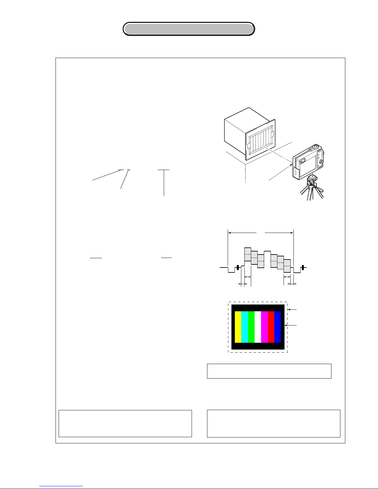
1. Connection
2. Adjust the distance so that the output waveform of
Fig. a and the Fig. b can be obtain.
When indicating parts by reference number, please
include the board name.
THIS NOTE IS COMMON FOR SCHEMATIC DIAGRAMS
(In addition to this, the necessary note is printed in each block)
Kinds of capacitor
Case Size
External dimensions (mm)
Note : Les composants identifiés par une marque
0 sont critiques pour la sécurité.
Ne les remplacer que par une pièce portant
le numéro spécifie.
Note : The components identified by mark 0 or
dotted line with mark 0 are critical for safety.
Replace only with part number specified.
Fig.b (Picture on monitor TV)
H
A=B/2A
BB
A
Yellow
Cyan
Green
White
Magenta
Red
Blue
Fig. a (Video output terminal output waveform)
CRT picture frame
Electronic beam
scanning frame
4-2. SCHEMATIC DIAGRAMS
Front of the lens
L = About 27 cm (PTB-450)
L = About 11 cm (PTB-1450)
L
Pattern box
DSC-W1/W12
Note:CD-507 flexible complete board and IC101 are not
supplied, but there are included in CCD block assy.
Note: Voltage and Waveform of mounted on CD-507 flexible
board can not be measured, because they are mounted
by the side of the lens.
16V
XX
C104
16V
0.1u
C107
16V
0.1u
C110
XX
C105
16V
0.1u
C108
C102
XX
R102
68
3900
R104
3900
R110
10V
C106
0.1u
R113
22k
R112
820
LND139
X_LED
LND138
M_5V
LND137
GND
LND112
GND
LND136
V1A
LND135
V1B
LND134
V2
LND118
CCD_GND
LND102
GND
LND103
GND
LND104
RG
LND116
CCD_OUT
LND106
H2A
LND109
H1A
LND127
VHOLD
LND120
VSUB_CONT
LND128
V5B
LND105
GND
LND107
H2B
LND108
GND
LND131
VST
LND133
V3A
LND101
CAM_-7.5V
LND129
V5A
LND123
V8
LND126
V6
LND124
V7B
LND119
POWER_SAVE
LND122
GND
LND111
GND
LND121
VSUB
LND125
V7A
LND132
V3B
LND117
NC
LND130
V4
LND115
GND
LND113
CAM_15V
LND114
GND
LND110
H1B
ICX455CQZ-13
IC101
1
V1A
2NC3
V1B
4V25
V3A
6
V3B
7
Vst
8V49
V5A
10
V5B
11
Vhld
12V613
V7A
14
V7B
15V816
NC
17
VOUT18NC19GND(Rss3)20GND21GND22VDD23RG24H2B25H1B26SUB27CSUB28NC29VL30H1A31H2A32NC
FB101
FB102
CL107
CL108
2SC39320S2S0
Q102
DTC144EMT2L
Q105
DTC144EMT2L
Q103
CL109
OPY5052
D101
1
A
22
18
29
17
25
7
28
3
14
11
4
16
24
26
12
15
31
6
21
9
13
2
5
20
32
27
1
19
23
8
30
10
36
34
39
37
38
35
33
(1/6)
SY-102
PAGE 4-12
CN701
of LEVEL3
SWITCH
SWITCH
BUFFER
(SELF TIMER/AF ILLUMINATOR)
CCD IMAGER
IC101
Y/CHROMA
REC
VIDEO
SIGNAL
SIGNAL PATH
CCD IMAGER (CCD BLOCK)
E
5
CD-507 FLEXIBLE BOARD
7
G
4
C
6
05
89
B
3
D
F
XX MARK:NO MOUNT
2
For Schematic Diagram
• Refer to page 4-37 for printed wiring board.
4-7 4-8
CD-507
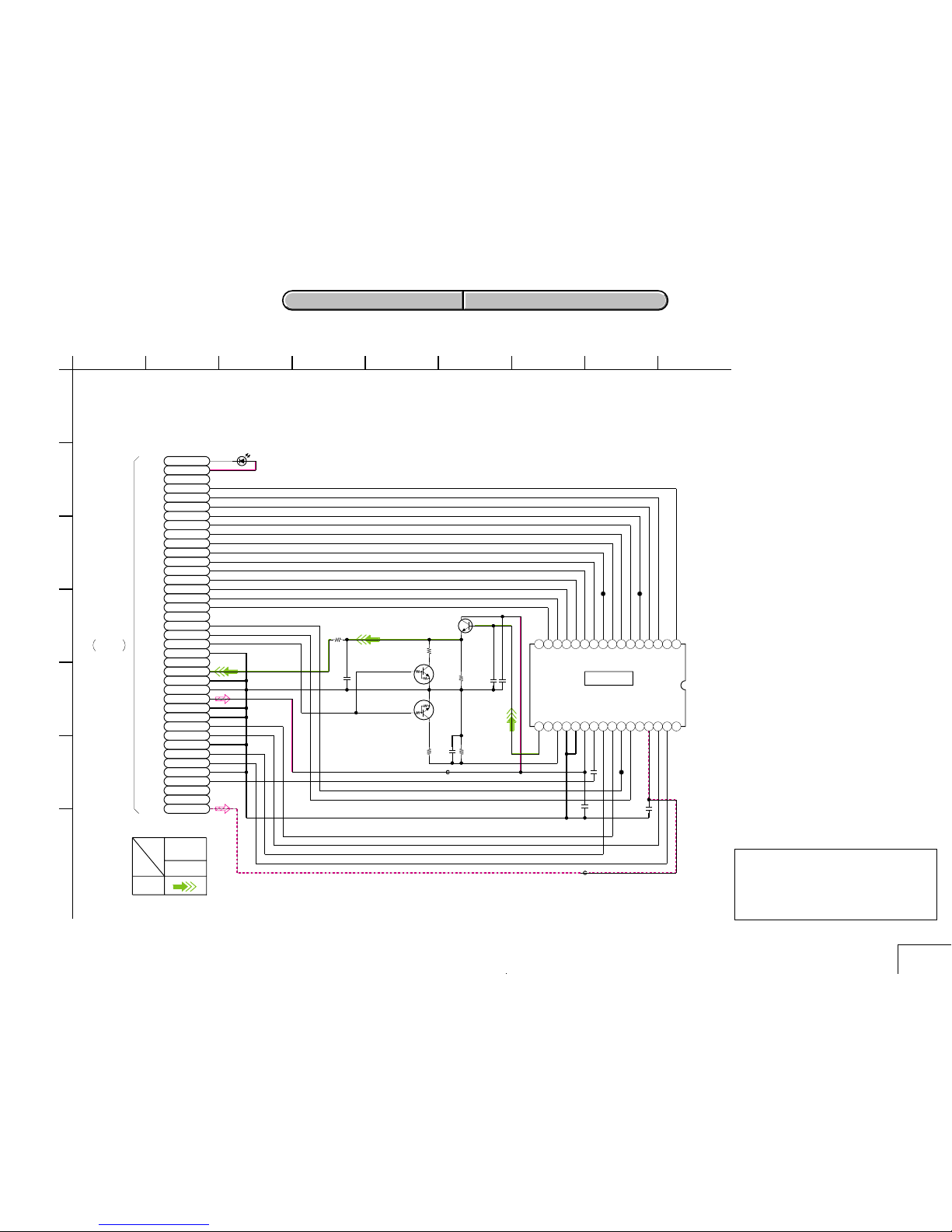
4-2. SCHEMATIC DIAGRAMS CD-507 FLEXIBLE BOARD
4-2. SCHEMATIC DIAGRAMS CD-507 FLEXIBLE BOARD
Precautions for Replacement of CCD Imager
• If the CCD imager has been replaced, carry out all the
adjustments for the camera section.
• As the CCD imager may be damaged by static electricity from
its structure, handle it carefully like for the MOS IC.
In addition, ensure that the receiver is not covered with dusts
nor exposed to strong light.

Schematic diagrams of the CH-146, SY-102, SW-422, MS-204, MS-205 flexible,
JK-263 and SP-045 flexible boards are not shown.
Pages from 4-9 to 4-28 are not shown.
DSC-W1/W12
0
280
0
0
0
0
0
05
0
NO MARK:REC/PB MODE
Note: ST-100 board is included in
ST-101 flexible complete board.
Note:ST-101 flexible complete
board is including ST-100
board.
Note:If C102 or C103 was damaged,
be sure to replace both C102
and C103 together.
(Note) (Note)
CPH3235-TL-E
Q001
1/16W
47
R009
MCH3405-TL-E
Q002
1
2
3
10k
R007
0.22u
C002
MA111-(K8).S0
D004
CY25BAJ-8F-T23
Q003
1
8
5
2
34
6
7
T001
4
1
3
2
5
150
R008
0.1u
C003
1M
R011
HAU160C030STP
D005
6.3V
10u
C001
100k
R005
2700
R004
47000pF
C005
2200
R006
TND721MH5-S-TL-E
IC001
1
NC
2
OUT
3
VDD
4
IN
5
GND
1M
R010
CL001
CL005CL004
CL042 CL007
CL006
CL003
CL009CL008 CL010
CL011 CL013CL012
CL014 CL015 CL016
CL017 CL019CL018
CL022
CL023
CL025
CL026
CL027
CL028
CL029
CL030
CL044
CL045
CL036
CL032
CL035
CL034
CL031
CL037
CL033
CL038
CL039
CL040
CL041
CL046
CL047
CL049
CL048
CL050
CL051
CL053
CL054
CL055
CL052
CL056
CL017
CL008
CL044
CL026
CL037
CL034
CL016
CL005
LND003
CL033
CL006
LND117
ST_UNREG
CL030
CL022
CL013
LND113
ST_UNREG
CL001
LND107
REG_GND
LND105
REG_GND
CL045
CL021
CL038
CL031
CL027
CL014
LND115
ST_UNREG
LND103
XSTRB_PWR_SAVE
CL023
LND109
REG_GND
CL018
LND004
LND002
XE_L
C102
43u
315V
CL028
CL007
CL019
LND110
REG_GND
LND102
ST_5V
LND001
XE_H
CL024
CL012
CL015
LND104
STB_FULL
CL036
CL004
CL011
LND116
ST_UNREG
CL039
LND114
ST_UNREG
LND106
REG_GND
C103
92u
315V
LND108
REG_GND
CL009
CL035
CL042
CL025
CL032
CL003
CL040
CL043
CL029
CL010
LND111
REG_GND
LND1011
2
3
4
5
6
7
8
9
10
11
12
13
14
15
16
17
STB_ON
CL041
LND112
ST_UNREG
CL048
CL054
CL055
CL047
CL046
CL056
CL051
CL053
CL050
CL049
CL052
1
A
F
P
S
STB_ON
ST_5V
XSTB_PWRSAVE
XSTB_FULL
REG_GND
ST_UNREG
REG_GND
REG_GND
REG_GND
REG_GND
REG_GND
ST_UNREG
ST_UNREG
ST_UNREG
ST_UNREG
ST_UNREG
TRIGGER 300V
TRIGGER GND
REG_GND
ST_UNREG
ST_UNREG
TRIGGER GND
TRIGGER 300V
FLASH
UNIT
of LEVEL3
CN601
SY-102
PAGE 4-18
(4/6)
C102,C103
CHARGING
CAPACITOR
IC001
FLASH CONTROL
TRANS DRIVE
TRANS DRIVE
FLASH DRIVE
FLASH DRIVE
ST-100 BOARD
CHARGING CAPACITOR,
FLEXIBLE
ST-101
BOARD
FLASH UNIT
D
F
B
E
5
J
3
H
C
62 9117
G
410
I
05
K
8
CL021
CL043
CL024
XE_H
XE_L
12
4-29
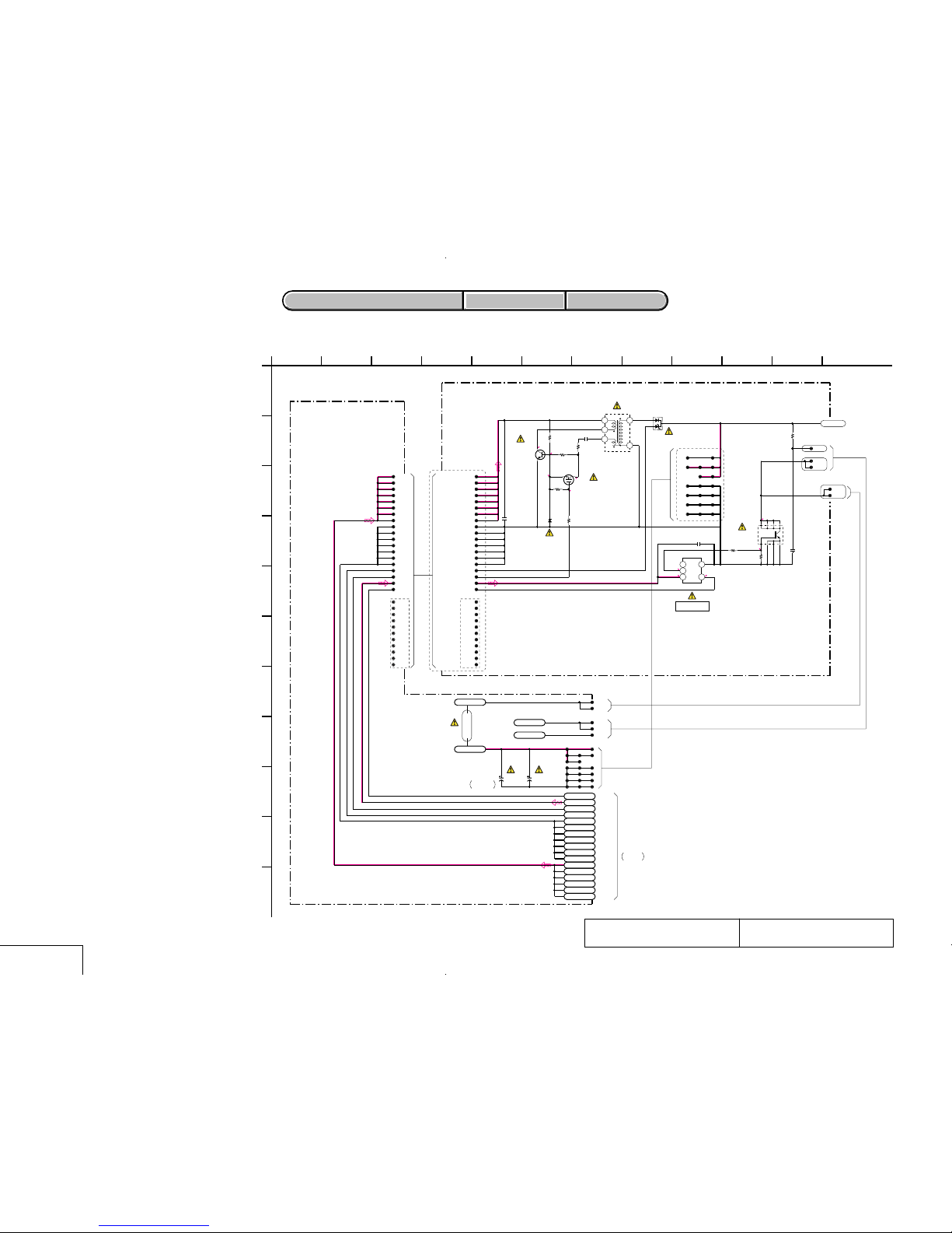
4-2. SCHEMATIC DIAGRAMS ST-100 BOARD
ST-101 FLEXIBLE BOARD
4-2. SCHEMATIC DIAGRAMS ST-100 BOARD
ST-101 FLEXIBLE BOARD
For Schematic Diagram
• Refer to page 4-49 for printed wiring board.
4-30
ST-100, ST-101
The components identified by mark 0 or dotted
line with mark 0 are critical for safety.
Replace only with part number specified.
Les composants identifiés par une marque 0 sont
critiques pour la sécurité. Ne les remplacer que
par une piéce portant le numéro spécifié.
DSC-W1/W12
LND001
STATIC_GND
S001
R001
1200
MAZS068008SO
D001
S002
CN001
9P
VCC
1
89
67
D-
2
D+
3
ID 4
GND
5
10k
R004
0uH
LF001
D004
XX
LND002
LND003
LND004
LND005
LND006
LND007
LND008
LND009
LND010
LND011
LND012
LND013
LND014
LND015
LND016
LND017
LND018
LND019
LND020
LND021
LND022
LND023
LND024
LND025
LND026
LND027
LND028
LND029
LND030
LND031
LND032
LND033
LND034
LND035
LND036
LND110
LND111
LND112
LND113
LND114
LND115
LND116
LND117
LND118
LND119
LND120
LND121
LND122
LND123
LND124
LND125
LND126
LND127
LND128
LND129
LND130
LND131
LND132
LND133
LND134
BT001
1
A
USBPHY_D+
USB_JACK_IN
KEY_AD2
REG_GND
USB_GND
USB_GND
AU_AIN
AU_2.8V
KEY_AD1
BEEP
REG_GND
REG_GND
REG_GND
SYS_SO
REG_GND
KEY_AD0
AU_SEN
AU_OUT
REG_GND
REG_GND
SP-
REG_GND
VL_3V
AU_AOUT
REG_GND
XSYS_SCK
XAU_LINE_MUTE
AU_5V
SP+
NC
XAU_LINE_MUTE
SYS_SO
SP+
AU_AOUT
AU_SEN
REG_GND
BEEP
KEY_AD1
SP-
KEY_AD0
XSYS_SCK
REG_GND
AU_OUT
REG_GND
REG_GND
REG_GND
REG_GND
REG_GND
AU_AIN
AU_2.8V
1
2
3
4
5
6
7
8
9
10
11
12
13
14
15
16
17
18
19
20
21
22
23
24
25
26
27
28
29
30
31
1
2
3
4
14
22
20
7
12
21
19
25
24
15
13
16
11
18
23
10
17
8
9
5
6
32
33
N.C2627
REG_GND
N.C
REG_GND
A_2.8VA_2.8V
AU_5V
AU_5V
AU_5V
USBPHY_D-
SIGNAL PATH
PB
REC
VIDEO SIGNAL
AUDIO
SIGNAL
Y/CHROMA
T(ZOOM)W
(USB)
BATTERY
LITHIUM
of LEVEL3
CN101
SW-422
PAGE 4-24
CN703
of LEVEL3
PAGE 4-19
(5/6)
SY-102
USB CONNECTOR (US BLOCK)
E
5
US-011 FLEXIBLE BOARD
G
4
H
C
6
05
B
3
D
F
XX MARK:NO MOUNT
2
4-32
For Schematic Diagram
• Refer to page 4-51 for printed wiring board.
US-011, CONTROL SWITCH
4-31
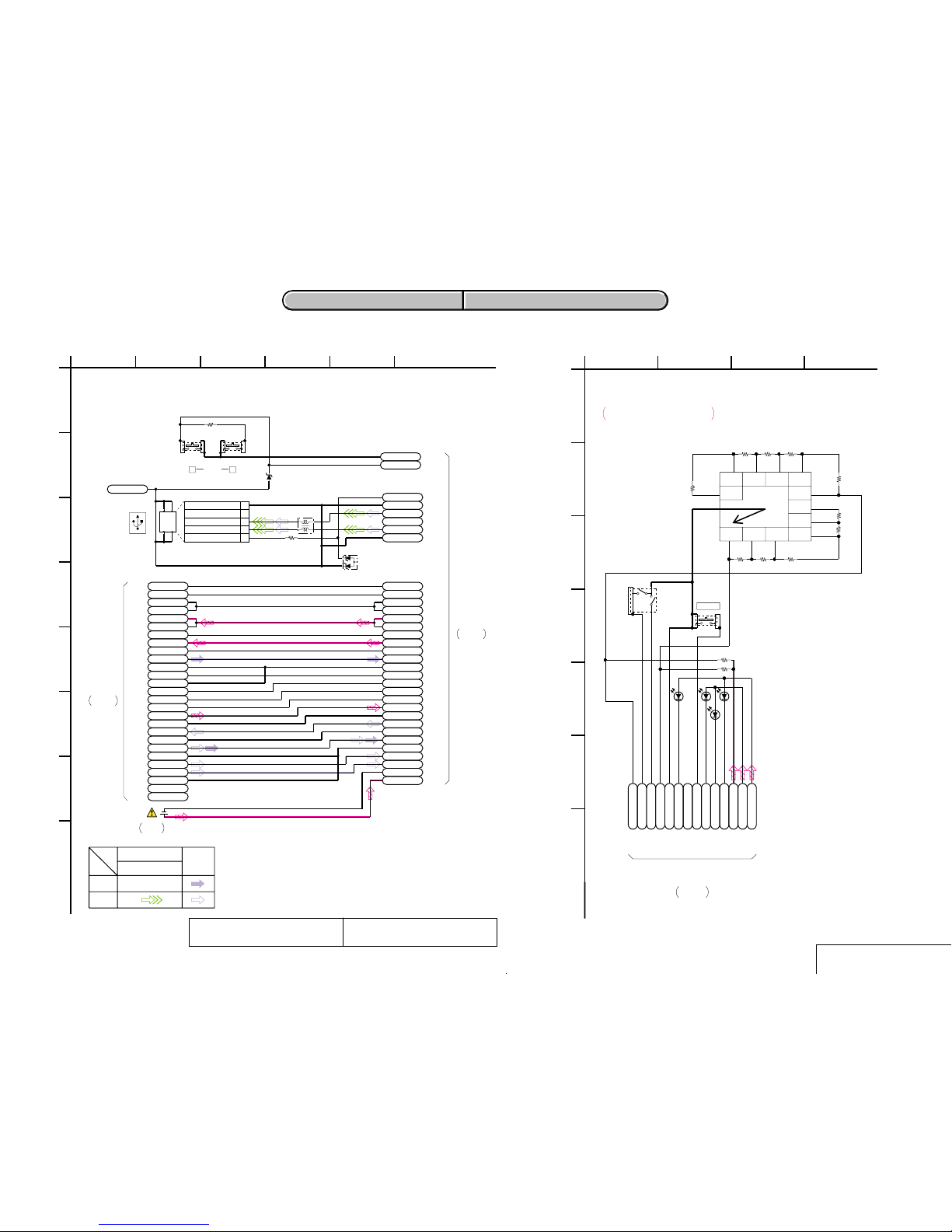
4-2. SCHEMATIC DIAGRAMS US-011 FLEXIBLE BOARD
4-2. SCHEMATIC DIAGRAMS US-011 FLEXIBLE BOARD
The components identified by mark 0 or dotted
line with mark 0 are critical for safety.
Replace only with part number specified.
Les composants identifiés par une marque 0 sont
critiques pour la sécurité. Ne les remplacer que
par une piéce portant le numéro spécifié.
CONTROL SWITCH BLOCK is replaced as block,
so that PRINTED WIRING BOARD is omitted.
S001
S002
LND001
LND005
LND002
LND007
LND009
LND006
LND010
LND004
LND003
LND012
LND011
R013
13.6k
R014
44k
6600
R011
44k
R004
13.6k
R007
6600
R009
LND008
LND013
LND014
2400
R006
2400
R012
3000
R008
3000
R010
D001
D004
D003
D002
20k
R016
20k
R015
1
A
(2nd)(1st)
POWER
614
9
857
2
101413
12 POSITION MODE_DIAL
XAE_LOCK_ON
XPWR_ON
MODE_DIAL0
XSHTR_ON
MODE_DIAL1
REG_GND
11
D_2.8V
XPWR_LED
12
3
123 4
5
6
7
891011
12
(POWER)
XTALLY_LED
XAE_LOCK_LED
XCHARGE_LED
(SELF TIMER/RECORDING)
(AE/AF LOCK)
(FLASH CHARGE)
EVER_3.0V
SET_UP MOVIE PLAY AUTO
P_AUTO
M
Twilight
Twilight
portrait
Candle
Landscape
Beach
Soft snap
D_2.8V
NC
SY-102
CN702
PAGE 4-20
(5/6)
of LEVEL3
(SHUTTER)
4
B
32
G
05
CONTROL SWITCH BLOCK
F
D
C
E
DSC-W1/W12
Link
Link
4-3. PRINTED WIRING BOARDS
ST-100 BOARD
ST-101 FLEXIBLE BOARD
US-011 FLEXIBLE BOARD
CD-507 FLEXIBLE BOARD
ST-100 BOARD
ST-101 FLEXIBLE BOARD
US-011 FLEXIBLE BOARD
CD-507 FLEXIBLE BOARD
CIRCUIT BOARDS LOCATION
COMMON NOTE FOR PRINTED WIRING BOARDS
MOUNTED PARTS LOCATION
CIRCUIT BOARDS LOCATION
COMMON NOTE FOR PRINTED WIRING BOARDS
MOUNTED PARTS LOCATION
Board Name Function
CD-507 FLEXIBLE CCD IMAGER
ST-100 FLASH DRIVE
ST-101 FLEXIBLE CHARGING CAPACITOR, FLASH UNIT
US-011 FLEXIBLE USB CONNECTOR
 Loading...