

Sony DSCP100 - Cybershot 5.1MP Digital Camera, Cyber-shot DSC-P120 Service Manual
SERVICE MANUAL
LEVEL 2
Link
SERVICE NOTE
DISASSEMBLY
BLOCK DIAGRAMS
FRAME SCHEMATIC DIAGRAM
SCHEMATIC DIAGRAMS
PRINTED WIRING BOARDS
REPAIR PARTS LIST
SPECIFICATIONS
SERVICE NOTE
DISASSEMBLY
BLOCK DIAGRAMS
FRAME SCHEMATIC DIAGRAM
SCHEMATIC DIAGRAMS
PRINTED WIRING BOARDS
REPAIR PARTS LIST
SPECIFICATIONS
Link
Revision History
Revision History
DSC-P100/P120
How to use
Acrobat Reader
How to use
Acrobat Reader
•For ADJUSTMENTS (SECTION 6), refer to SERVICE MANUAL, ADJ (987673451.pdf).
•For INSTRUCTION MANUAL, refer to SERVICE MANUAL, LEVEL 1 (987673441.pdf).
• Reference No. search on printed wiring boards is available.
• Note in Lens Frame Installation
• Exchange Method of Barrier Assy
• HELP: Sheet attachment positions and procedures of processing the flexible boards/harnesses are shown.
Ver 1.0 2004.04
DIGITAL STILL CAMERA
On the CH-146 and SY-104 boards
This service manual procides the information that is premised
the circuit board replacement service and not intended repair
inside the CH-146 and SY-104 boards.
Therefore, schematic diagram, printed wiring board and
electrical parts list of the CH-146 and SY-104 boards are not
shown.
The following pages are not shown.
Schematic diagram ............ Pages 4-9 to 4-28
Printed wiring board ........... Pages 4-39 to 4-42
Mounted parts location....... Pages 4-50 and 4-51
Electrical parts list .............. Pages 5-6 and 5-8 to 5-12
The above-described information is shown in service
manual Level 3.
DSC-P100
US Model
Canadian Model
E Model
Hong Kong Model
Australian Model
Chinese Model
Korea Model
Tourist Model
Japanese Model
DSC-P100/P120
AEP Model
UK Model
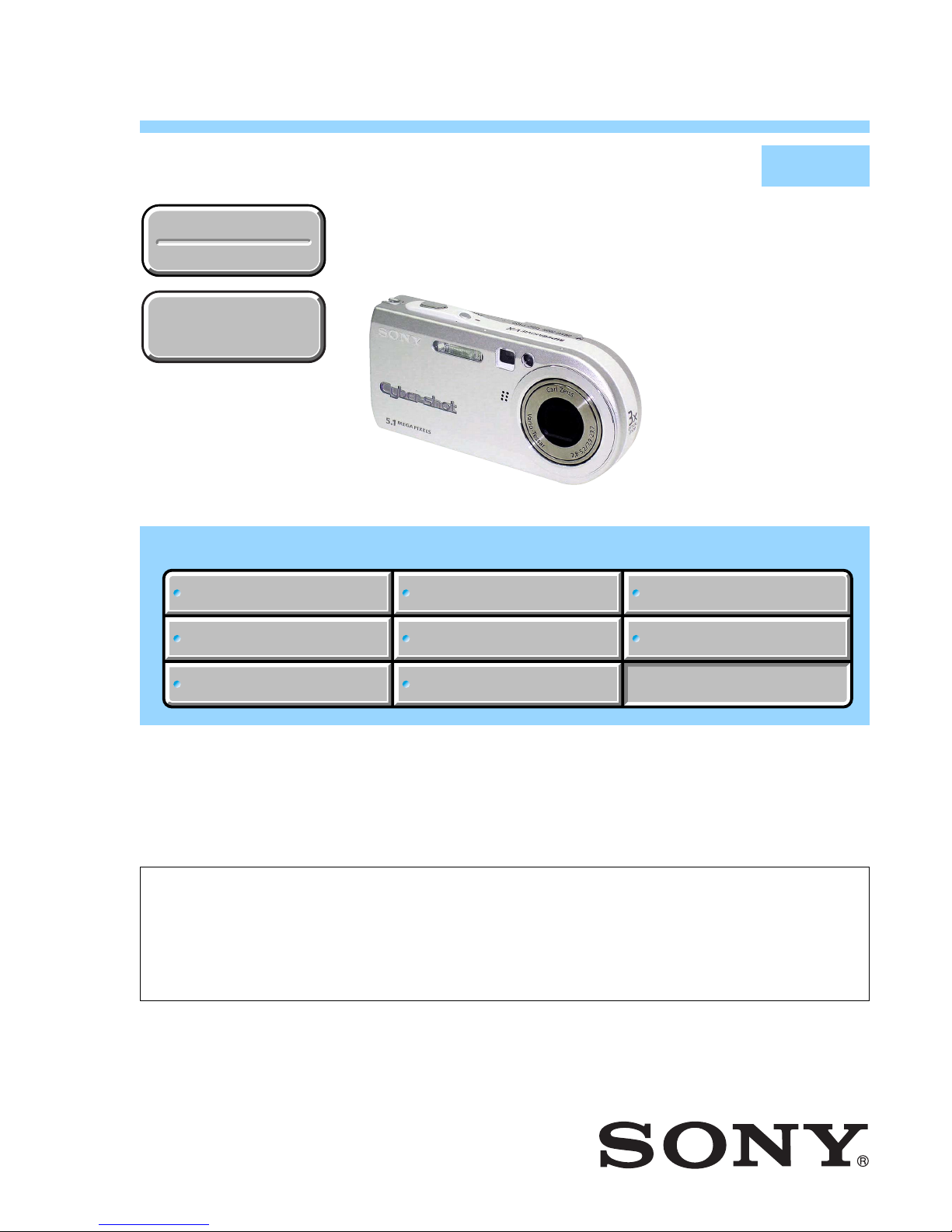
Photo: DSC-P100/Silver

— 2 —
DSC-P100/P120
SPECIFICATIONS
[Input and Output connectors]
Multi connector
USB communication
Hi-Speed USB (USB 2.0 complia nt)
[LCD screen]
LCD panel
4.6 cm (1.8 type) TFT drive
Total number of dots
134 000 (560×240) dots
[Power, general]
Used battery pack
NP-FR1
Power requirements
3.6 V
Power consumption (d uring shoot ing with
LCD screen on)
1.3 W
Operating temperature
0°C to +40°C (+32°F to +104°F)
Storage temperature
–20°C to +60°C (–4°F to +140°F)
Dimensions
108×51.5×26.6 mm
(4 3/8×2 1/8×1 1/16 inches)
(W/H/D, excluding maximum
protrusions)
Mass Approx. 183 g (6.5 oz) (including
battery pack NP-FR1, “Memory
Stick” and wrist strap)
Microphone
Electret condenser microphone
Speaker Dynamic speaker
Exif Print Compatible
PRINT Image Matching II
Compatible
PictBridge
Compatible
x AC-LS5/LS5B AC Adaptor
Input rating
100 V to 240 V AC, 50/60 Hz, 11 W,
0.16 A to 0.09 A
Output rating
4.2 V DC, 1.5 A
Operating temperature
0°C to +40°C (+32°F to +104°F)
Storage temperature
–20°C to +60°C (–4°F to +140°F)
Dimensions
Approx. 48×29×81mm
(1 15/16×1 3/16×3 1/4 inches)
(W/H/D, excluding projecting parts)
Mass Approx. 130 g (5 oz) excluding
power cord (mains lead)
x NP-FR1 battery pack
Used battery
Lithium-ion battery
Maximum voltage
DC 4.2 V
Nominal voltage
DC 3.6 V
Capacity 4.4 Wh (1220 mAh)
x Accessories
• AC-LS5/LS5B AC Adaptor (1)
• Power cord (mains lead) (1)
• NP-FR1 battery pack (DSC-P100:1, DSC-
P120:2)
• Battery case (DSC-P100:1, DSC-P120:2)
• USB multi cable (1)
• A/V multi cable (1)
• Wrist strap (1)
• “Memory Stick” (32 MB) (1)
• CD-ROM (USB driver SPVD-012) (1)
• Operating instructions (1)
• Soft carrying case (DSC-P120 only) (1)
See page 5-13.
Design and specifications are subject to change
without notice.
x Camera
[System]
Image device
9.04 mm (1/1.8 type) color CCD
Primary color filter
Total pixels numbe r of came ra
Approx. 5 255 000 pixels
Effective pixels number of camera
Approx. 5 090 000 pixels
Lens Carl Zeiss Vario-Tessar
3× zoom lens
f = 7.9 – 23.7 mm (38 – 114 mm when
converted to a 35 mm still camera)
F2.8 – 5.2
Exposure control
Automatic exposure, Manual
exposure, Scene selection (9 modes)
White balance
Automatic, Daylight, Cloudy,
Fluorescent, Incandescent, Flash
File format (DCF compliant)
Still images: Exif Ver. 2.2 JPEG
compliant, DPOF compatible
Movies: MPEG1 compliant
(Monaural)
Recording media
“Memory Stick”
Flash Recommended distance (ISO set to
Auto):
0.2m to 3.5 m (7 7/8 inches to 11 feet
53/4 inches) (W)
0.3m to 2.5 m (11 7/8 inches to 8 feet
23/8 inches) (T)

— 3 —
DSC-P100/P120
1. Check the area of your repair for unsoldered or poorly-soldered
connections. Check the entire board surface for solder splashes
and bridges.
2. Check the interboard wiring to ensure that no wires are
"pinched" or contact high-wattage resistors.
3. Look for unauthorized replacement parts, particularly
transistors, that were installed during a previous repair . Point
them out to the customer and recommend their replacement.
4. Look for parts which, through functioning, show obvious signs
of deterioration. Point them out to the customer and
recommend their replacement.
5. Check the B+ voltage to see it is at the values specified.
6. Flexible Circuit Board Repairing
•Keep the temperature of the soldering iron around 270˚C
during repairing.
• Do not touch the soldering iron on the same conductor of the
circuit board (within 3 times).
• Be careful not to apply force on the conductor when soldering
or unsoldering.
Unleaded solder
Boards requiring use of unleaded solder are printed with the leadfree mark (LF) indicating the solder contains no lead.
(Caution: Some printed circuit boards may not come printed with
the lead free mark due to their particular size.)
: LEAD FREE MARK
Unleaded solder has the following characteristics.
• Unleaded solder melts at a temperature about 40°C higher than
ordinary solder.
Ordinary soldering irons can be used but the iron tip has to be
applied to the solder joint for a slightly longer time.
Soldering irons using a temperature regulator should be set to
about 350°C.
Caution: The printed pattern (copper foil) may peel away if the
heated tip is applied for too long, so be careful!
• Strong viscosity
Unleaded solder is more viscous (sticky , less prone to flo w) than
ordinary solder so use caution not to let solder bridges occur such
as on IC pins, etc.
• Usable with ordinary solder
It is best to use only unleaded solder but unleaded solder may
also be added to ordinary solder.
SAFETY CHECK-OUT
After correcting the original service problem, perform the following
safety checks before releasing the set to the customer.
SAFETY-RELATED COMPONENT WARNING!!
COMPONENTS IDENTIFIED BY MARK 0 OR DOTTED LINE WITH
MARK 0 ON THE SCHEMATIC DIAGRAMS AND IN THE PARTS
LIST ARE CRITICAL TO SAFE OPERATION. REPLACE THESE
COMPONENTS WITH SONY PARTS WHOSE PART NUMBERS
APPEAR AS SHOWN IN THIS MANUAL OR IN SUPPLEMENTS
PUBLISHED BY SONY .
ATTENTION AU COMPOSANT AYANT RAPPORT
À LA SÉCURITÉ!
LES COMPOSANTS IDENTIFÉS P AR UNE MARQUE 0 SUR LES
DIAGRAMMES SCHÉMA TIQUES ET LA LISTE DES PIÈCES SONT
CRITIQUES POUR LA SÉCURITÉ DE FONCTIONNEMENT. NE
REMPLACER CES COMPOSANTS QUE PAR DES PIÈSES SONY
DONT LES NUMÉROS SONT DONNÉS DANS CE MANUEL OU
DANS LES SUPPÉMENTS PUBLIÉS PAR SONY.

— 4 —
DSC-P100/P120
TABLE OF CONTENTS
1. SERVICE NOTE
1-1. Note for Repair ································································1-1
1-2. Discharging of the ST-105 Flexible Board’s Charging
Capacitor (C550) ·····························································1-1
1-3. Note in Lens Frame Installation ······································1-2
1-4. Description on Self-diagnosis Display ···························· 1-2
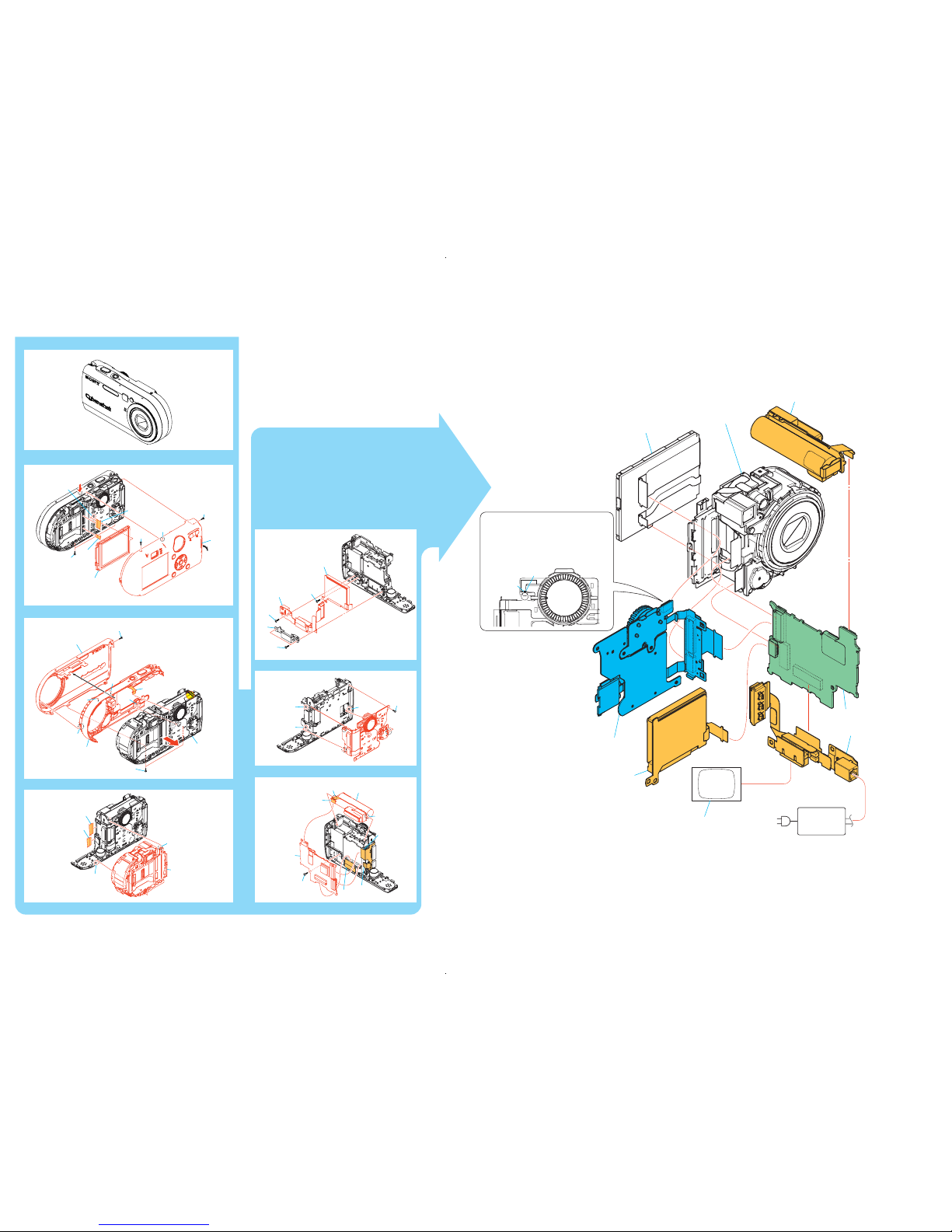
2. DISASSEMBLY
2-1. Flow Chart ·······································································2-1
2-2. SY-104 Board Service Position ·······································2-3
2-3. Exchange Method of Barrier Assy ··································2-5
2-3-1.Peel Off Old Ornamental Ring A ····································2-5
2-3-2.Remove Old Barrier Assy················································2-6
2-3-3.Install New Barrier Assy ·················································2-6
2-3-4.Adhere the Ornamental Ring A ·······································2-7
2-4. Circuit Boards Location ·················································· 2-8
3. BLOCK DIAGRAMS
3-1. Overall Block Diagram (1/2)···········································3-1
3-2. Overall Block Diagram (2/2)···········································3-3
3-3. Power Block Diagram (1/2)·············································3-5
3-4. Power Block Diagram (2/2)·············································3-7
4. PRINTED WIRING BOARDS AND
SCHEMATIC DIAGRAMS
4-1. Frame Schematic Diagram ··············································4-1
4-2. Schematic Diagrams························································4-5
CD-511 FLEXIBLE (CCD IMAGER) ··························· 4-7
ST-105 FLEXIBLE (CHARGING CAPACITOR) ·······4-29
ST-102 (FLASH DRIVE) ············································· 4-29
MS-207 FLEXIBLE
(MEMORY STICK CONNECTOR) ····························4-31
JK-266 FLEXIBLE
(DC IN, MULTI CONNECTOR) ································· 4-32
CONTROL SWITCH BLOCK (SW), (RL) ·················4-33
4-3. Printed Wiring Boards ··················································· 4-35
CD-511 FLEXIBLE ······················································4-37
ST-105 FLEXIBLE ·······················································4-43
ST-102 ···········································································4-44
MS-207 FLEXIBLE ······················································ 4-45
JK-266 FLEXIBLE ······················································· 4-46
4-4. Mounted Parts Location ················································ 4-49
5. REPAIR PARTS LIST
5-1. Exploded Views·······························································5-2
5-1-1.Cabinet Block Section·····················································5-2
5-1-2.Lens Block Section··························································5-3
5-1-3.BT Holder Block Section ················································ 5-4
5-2. Electrical Parts List ·························································5-5
Section Title Page
1-1
SECTION 1
SERVICE NOTE
DSC-P100/P120
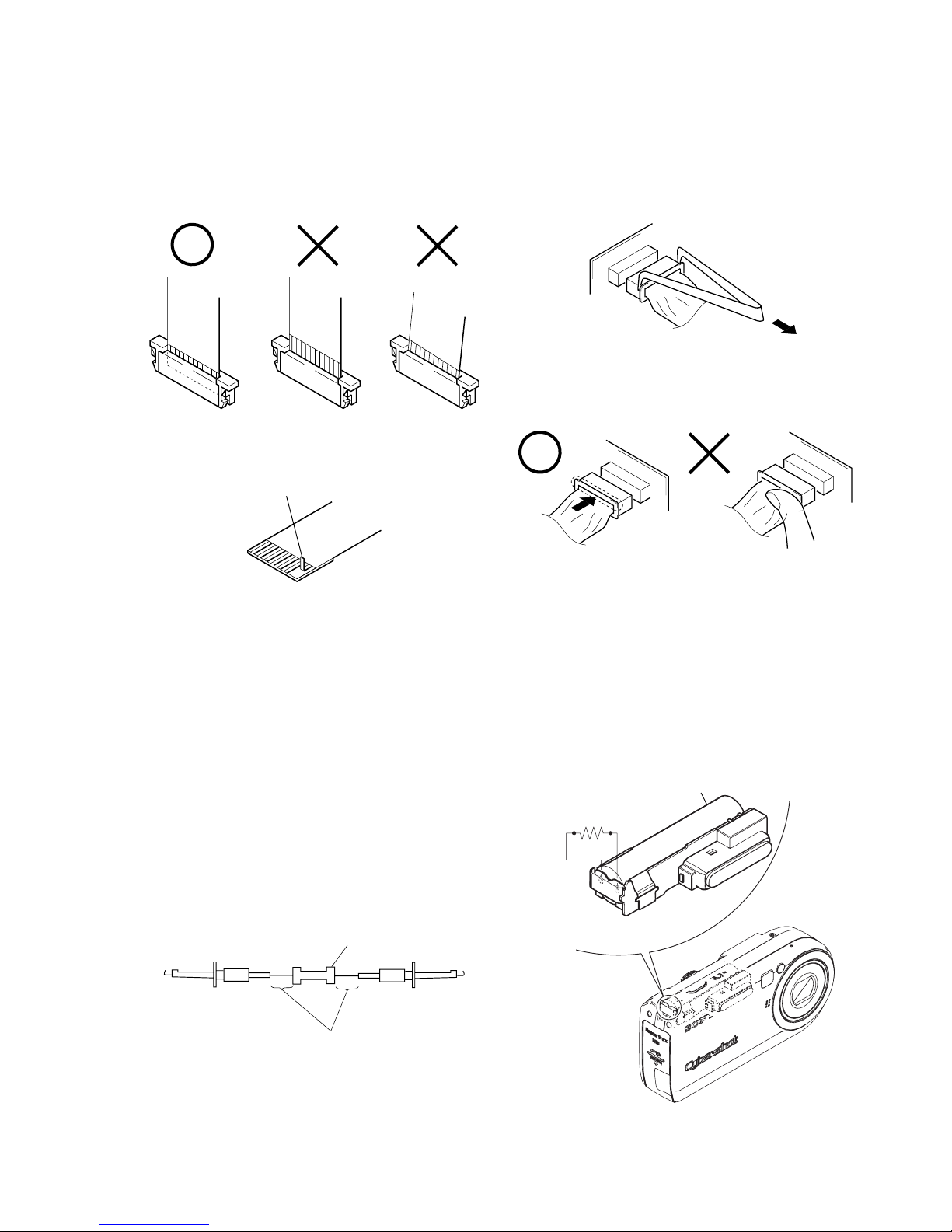
1-2. DISCHARGING OF THE ST-105
FLEXIBLE BOARD’S CHARGING
CAPACITOR (C550)
The charging capacitor (C550) of the ST-105 flexible board is
charged up to the maximum 300 V potential.
There is a danger of electric shock by this high voltage when the
capacitor is handled by hand. The electric shock is caused by the
charged voltage which is kept without discharging when the main
power of the unit is simply turned off. Therefore, the remaining
voltage must be discharged as described below.
Preparing the Short Jig
To preparing the short jig, a small clip is attached to each end of a
resistor of 1 kΩ /1 W (1-215-869-11).
Wrap insulating tape fully around the leads of the resistor to prevent
electrical shock.
1 kΩ/1 W
Wrap insulating tape.
Discharging the Capacitor
Short-circuit between the positive and the negative terminals of
charged capacitor with the short jig about 10 seconds.
1-1. NOTE FOR REPAIR
Make sure that the flat cable and flexible board are not cracked of
bent at the terminal.
Do not insert the cable insufficiently nor crookedly.
Cut and remove the part of gilt
which comes off at the point.
(Be careful or some
pieces of gilt may be left inside)
When remove a connector, don’t pull at wire of connector.
It is possible that a wire is snapped.
When installing a connector, don’t press down at wire of connector.
It is possible that a wire is snapped.
R:1 kΩ/1 W
(Part code:
1-215-869-11)
Capacitor
ST-105
1-2E
DSC-P100/P120
Display Code
1-4. DESCRIPTION ON SELF-DIAGNOSIS DISPLAY
Self-diagnosis display
• C: ss: ss
You can reverse the camera
malfunction yourself. (However,
contact your Sony dealer or local
authorized Sony service facility
when you cannot recover from the
camera malfunction.)
• E: ss: ss
Contact your Sony dealer or local
authorized Sony service facility.
1-3. NOTE IN LENS FRAME INSTALLATION
When tightening a screw, have both sides of the lens block assembly so as not for the load to depend.
M1.7 × 4
Lens frame
Lens block assembly
C:32:ss
C:13:ss
Countermeasure
Turn the power off and on again.
Format the “Memory stick”.
Insert a new “Memory Stick”.
Cause
Trouble with hardware.
Unformatted memory stick is inserted.
Memory stick is broken.
Caution Display During Error
SYSTEM ERROR
FORMAT ERROR
MEMORY STICK ERROR
E:61:ss
E:91:ss
Checking of lens drive circuit.
When failed in the focus and zoom
initialization.
Abnormality when flash is being
charged.
Checking of flash unit or replacement
of flash unit.
—
DSC-P100/P120
2-1 2-2
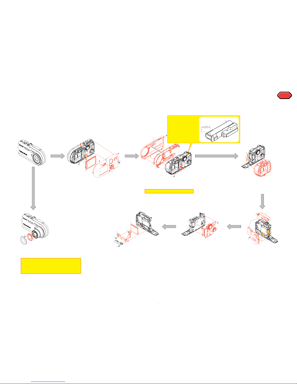
2-1. FLOW CHART
The following flow chart shows the disassembly procedure.
SECTION 2
DISASSEMBLY
HELP
HELP
Note: Mic harness is connected.
Note: When you exchange rings, be sure
to follow the procedure carried on
"2-3. Exchange Method of Barrier
Assy" (2-5 page).
1 Control switch block (RL): CN003
2 Screw (M1.4)
x3
3 Main block assy
4 Mic harness: CN707
5 Claw
x3
6 Front cabinet
7 Control switch block (RL)
1 ST-105 flexible: CN706
2 Claw
x2
3 ST-105
4 JK-266 flexible: CN704
5 Tapping screw (M1.7)
x1
6 Control switch block (SW): CN703
7 MS-207 flexible: CN751
8 SY-104
1 Screw (M1.4)
x1
2 Claw
x1
3 Claw
x2
4 Remove the Control switch block (SW)
in the direction of arrow A.
1 Tapping screw (M1.7)
x3
2 Multi fixed plate
3 JK-266
4 Tapping screw (M1.7)
x1
5 MS-207
1 Ornamental ring A
2 Tapping screw (M1.2)
x2
3 Barrier assy
1 Claw
x2
2 CD-511: CN101
3 Lens block flexible: CN201
4 Lens block
6
7
1
2
4
3
1
1
2
1
2
1
4
2
1
3
1
2
3
5
3
3
3
5
5
5
2
3
1 Screw (M1.4)
x4
2 Remove the boss, pushing A portion.
3 Remove the rear cabinet from battery lid side.
4 Claw
x1
5 Rear cabinet
6 Panel block assy
7 LCD flexible: CN001
8 Back light flexible: CN002
6
1
4
3
8
7
2
A
A
1
1
5
4
1
2
2
4
7
8
5
6
Note: High-voltage cautions
Discharging the Capacitor
Short-circuit between the two
points with the short jig about 10
seconds.
R:1 kΩ/1 W
(Part code:
1-215-869-11)
Capacitor
ST-105
DSC-P100/P120
2-3 2-4
2-2. SY-104 BOARD SERVICE POSITION
Lens block
Panel block
To turn on/off the power, short
the circuit between pin 5 and
pin 6 (GND) of CN003 on Control
switch block (SW) for 1 second.
CN003
6
5
ST-105 flexible board
MS-207 flexible board
JK-266 flexible board
SY-104 board
Control switch block (SW)
Color monitor
A/V multi cable
AC power
adaptor
AC IN
5
1
4
3
7
6
2
A
1
1
6
7
1
2
4
3
5
5
5
2
1
1
2
3
4
3
1
2
2
4
7
8
5
6
1
2
3
3
A
1
4
2
1
3
5
2-5
DSC-P100/P120
2-3. EXCHANGE METHOD OF BARRIER ASSY
Service parts
Part Number Part Name Quantity
1 3-091-427-01 Ring (A), Ornamental 1
2 X-3954-476-1 Barrier Assy 1
3 3-086-156-31 Tapping screw (P2) 2
Tools used
Torque driver
Soldering iron
Weight about 60g
Adhesive (Super X) (Note)
Note: Use adhesive (Super X) or an equivalent article.
Don’t use what becomes white after drying like a quick-drying glue.
2-3-1. PEEL OFF OLD ORNAMENTAL RING A
The Ornamental Ring A has adhered to the Barrier Assy strongly and accordingly, use a soldering iron to weaken the adhesive force.
Heat four circled portions with the soldering iron.
Heating temperature is about 300ºC.
Beware of a burn since the entire Ornamental Ring becomes hot.
* As the adhesive force of Ornamental Ring A is considerably large, the forced peeling will damage the group-1 frame.
Insert the tip of tweezers, etc. into a notch of the group-1 frame and prize the ring.
* Take extreme care so as not to damage the coated surface of the group-1 frame.
In case of difficult peeling, heat the ring again with the soldering iron.
If this re-heating failed, it may be advisable that the ring be peeled while heating the portions 1 → 2 → 3 → 4 in the under figure one
by one sequentially.
* Discard the removed Ornamental Ring A.
1
2
3
1
Tip
3
4
2
2-6
DSC-P100/P120
2-3-2. REMOVE OLD BARRIER ASSY
1 Remove two screws.
* Discard the removed screws.
2 Remove the Barrier Assy.
* Discard the removed Barrier Assy.
* After removing the Barrier Assy, if the “G1 Dust-Proof Ring” was removed, it must be returned to the home position.
In returning the ring, adjust the location of a projection to the lens direction.
This is an important part to prevent the dust and light from coming in.
* After removing the Barrier Assy, take extreme care not to drop dust or foreign substances in the lens barrel.
2-3-3. INSTALL NEW BARRIER ASSY
1 Install new Barrier Assy by paying attention to the projection of the Barrier Assy in relation to the position shown in the under figure.
2 Tighten two screws.
* Tightening torque = 0.5 kgf
1
1
2
Projection
2
2
1
2-7
DSC-P100/P120
2-3-4. ADHERE THE ORNAMENTAL RING A
Apply an adhesive to four recesses on the top surface of the Barrier Assy.
* Do not apply too much adhesive. (Make quantity of adhesives into the quantity in which a groove hides.)
Meeting a “notch” of the Ornamental Ring A with a “projection” of the group-1 frame, push the Ornamental Ring A into the group-1 frame.
* The projection of the spring for preventing static electricity must be tilted.
Put the 60g weight on the Ornamental Ring A so that the Ornamental Ring A does not float up until the adhesive hardens.
Note: Be careful not to give a shock.
* After the weight was put, no gap must be present in full circumference between Ornamental Ring A and group-1 frame.
A gap, if present, causes the crackle sound NG.
* The weight must push in the Ornamental Ring A only.
If the weight is put on the mold part of the Barrier Assy, the Ornamental Ring A will float up.
Completion after 30 minutes.
Notch
Adhesive
Adhesive
Adhesive
Do not put the weight on a black mold part.
Not gap in full circumference.
Adhesive
Projection

2-8E
DSC-P100/P120
2-4. CIRCUIT BOARDS LOCATION
CD-511 flexible
SY-104
(including CH-146)
ST-105 flexible
(including ST-102)
CH-146
(included in SY-104)
MS-207 flexible
JK-266 flexible
Board Name Function
CD-511 flexible CCD IMAGER
CH-146 CCD SIGNAL PROCESS
(included in SY-104)
JK-266 flexible DC IN, MULTI CONNECTOR
MS-207 flexible MEMORY STICK CONNECTOR
ST-102 FLASH DRIVE
ST-105 flexible CHARGING CAPACITOR
SY-104 CAMERA MODULE, CAMERA DSP, LENS DRIVE,
(Including CH-146) SH DSP, FRONT CONTROL,
LCD DRIVE,
AUDIO,
DC/DC CONVERTER
DSC-P100/P120
HELP
CN751
SY spacer (MS)
Shield sheet (SY)
Battery holder assy
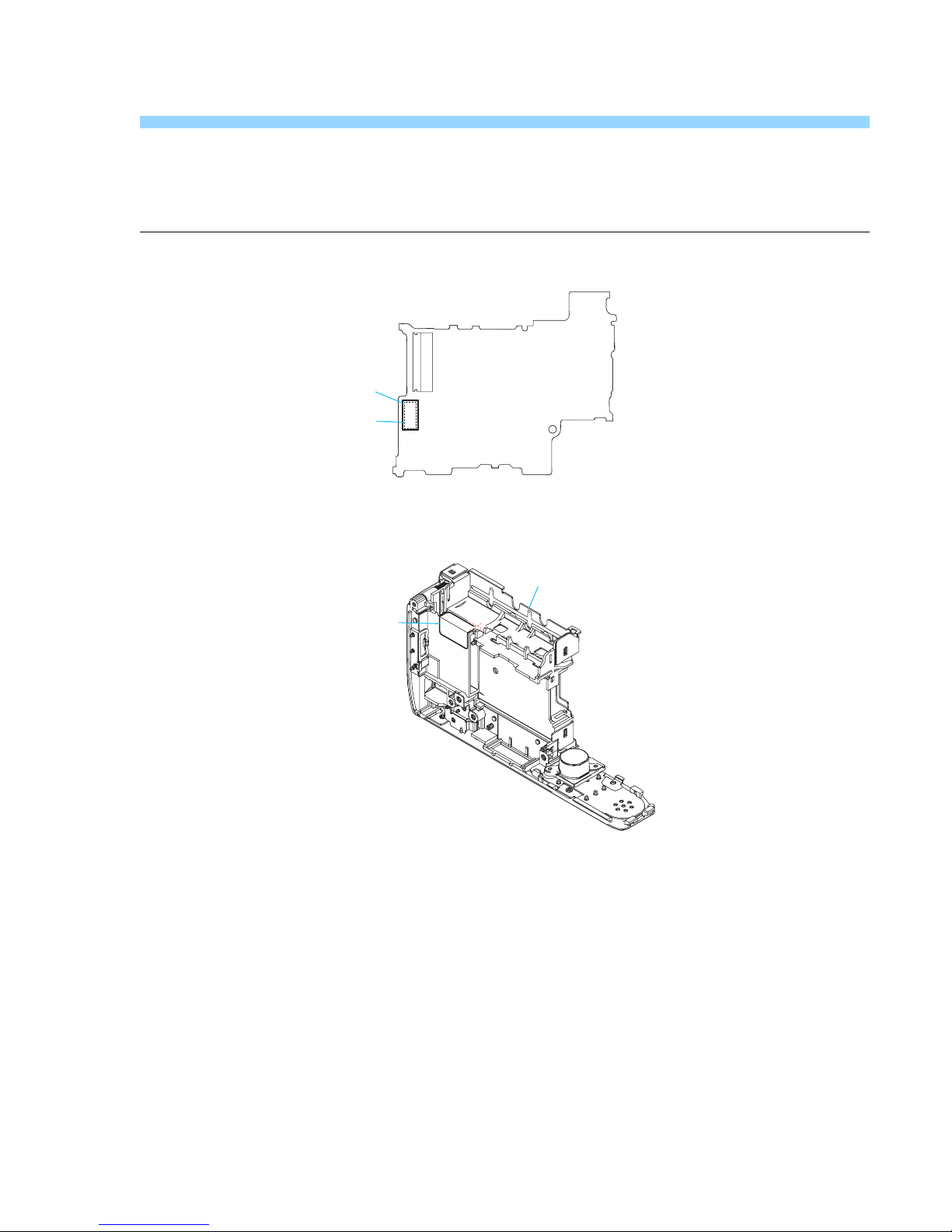
HELP
Sheet attachment positions and procedures of processing the flexible boards/harnesses are shown.

DSC-P100/P120
Link
Link
3. BLOCK DIAGRAMS
OVERALL BLOCK DIAGRAM (2/2) POWER BLOCK DIAGRAM (2/2)
POWER BLOCK DIAGRAM (1/2)OVERALL BLOCK DIAGRAM (1/2)
OVERALL BLOCK DIAGRAM (2/2) POWER BLOCK DIAGRAM (2/2)
POWER BLOCK DIAGRAM (1/2)OVERALL BLOCK DIAGRAM (1/2)
 Loading...