

SONY D-NE330, D44H-D, D18, D44H11G, D44H8G Service Manual
...
D44H Series (NPN),
D45H Series (PNP)
Preferred Devices
Complementary Silicon
Power Transistors
These series of plastic, silicon NPN and PNP power transistors can
be used as general purpose power amplification and switching such
as output or driver stages in applications such as switching regulators,
converters and power amplifiers.
Features
•Low Collector-Emitter Saturation Voltage
V
•Fast Switching Speeds
•Complementary Pairs Simplifies Designs
•Pb-Free Packages are Available*
MAXIMUM RATINGS
Collector-Emitter Voltage
D44H8, D45H8
D44H11, D45H11
Emitter Base Voltage V
Collector Current
- Continuous
- Peak (Note 1)
Total Power Dissipation
@ TC = 25°C
@ TA = 25°C
Operating and Storage Junction
Temperature Range
THERMAL CHARACTERISTICS
Thermal Resistance, Junction-to-Case
Thermal Resistance, Junction-to-Ambient
Maximum Lead Temperature for Soldering
Purposes: 1/8″ from Case for 5 Seconds
Stresses exceeding Maximum Ratings may damage the device. Maximum
Ratings are stress ratings only. Functional operation above the Recommended
Operating Conditions is not implied. Extended exposure to stresses above the
Recommended Operating Conditions may affect device reliability.
1. Pulse Width v 6.0 ms, Duty Cycle v 50%.
*For additional information on our Pb-Free strategy and soldering details, please
download the ON Semiconductor Soldering and Mounting Techniques
Reference Manual, SOLDERRM/D.
= 1.0 V (Max) @ 8.0 A
CE(sat)
Rating Symbol Value Unit
V
CEO
EB
I
C
P
D
TJ, T
stg
Characteristic Symbol Max Unit
R
q
JC
R
q
JA
T
L
60
80
5.0 Vdc
10
20
70
2.0
-55 to +150 °C
1.8 °C/W
62.5 °C/W
275 °C
Vdc
Adc
W
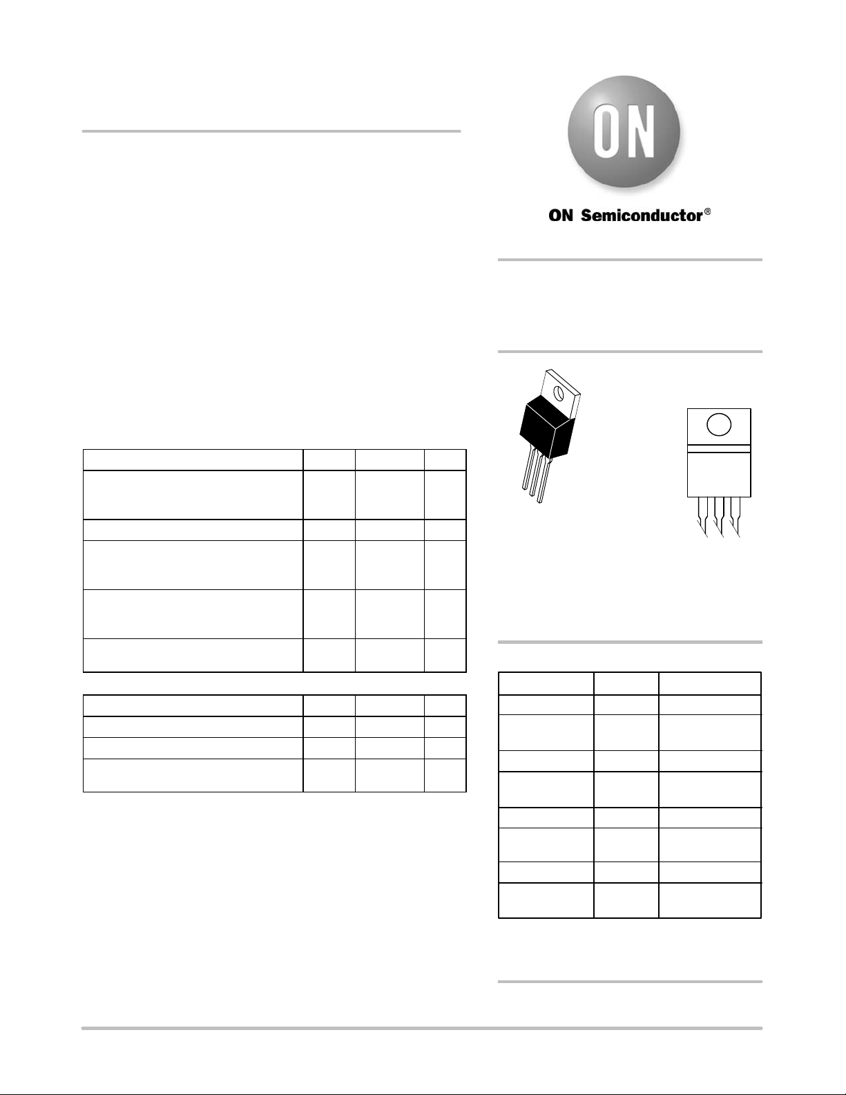
http://onsemi.com
10 AMP COMPLEMENTARY
SILICON POWER
TRANSISTORS 60, 80 VOLTS
4
TO-220AB
CASE 221A-09
1
2
3
D4xHyy = Device Code
A = Assembly Location
Y = Year
WW = Work Week
G = Pb-Free Package
STYLE 1
x = 4 or 5
yy = 8 or 11
ORDERING INFORMATION
Device Package Shipping
D44H8 TO-220
D44H8G TO-220
D44H11 TO-220 50 Units/Rail
D44H11G TO-220
D45H8 TO-220 50 Units/Rail
D45H8G TO-220
D45H11 TO-220 50 Units/Rail
D45H11G TO-220
†For information on tape and reel specifications,
including part orientation and tape sizes, please
refer to our Tape and Reel Packaging Specifications
Brochure, BRD8011/D.
Preferred devices are recommended choices for future use
and best overall value.
(Pb-Free)
(Pb-Free)
(Pb-Free)
(Pb-Free)
MARKING
DIAGRAM
D4xHyyG
AYWW
†
50 Units/Rail
50 Units/Rail
50 Units/Rail
50 Units/Rail
50 Units/Rail
© Semiconductor Components Industries, LLC, 2007
November, 2007 - Rev. 10
1 Publication Order Number:
D44H/D
D44H Series (NPN),
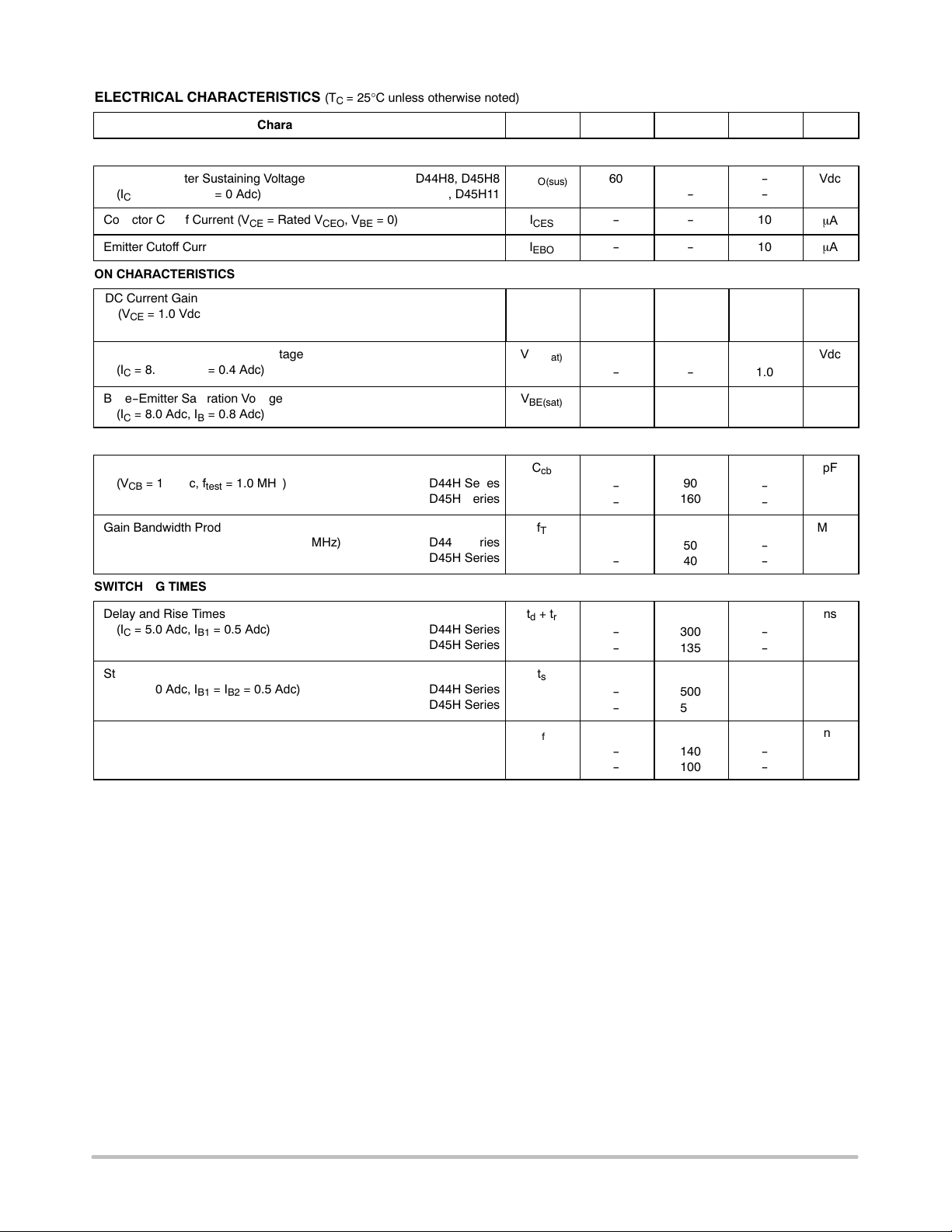
ELECTRICAL CHARACTERISTICS (T
= 25°C unless otherwise noted)
C
Characteristic
OFF CHARACTERISTICS
Collector-Emitter Sustaining Voltage D44H8, D45H8
(I
= 30 mAdc, IB = 0 Adc) D44H11, D45H11
C
Collector Cutoff Current (VCE = Rated V
, VBE = 0)
CEO
Emitter Cutoff Current (VEB = 5.0 Vdc)
ON CHARACTERISTICS
DC Current Gain
(VCE = 1.0 Vdc, IC = 2.0 Adc)
(VCE = 1.0 Vdc, IC = 4.0 Adc)
Collector-Emitter Saturation Voltage
(IC = 8.0 Adc, IB = 0.4 Adc)
Base-Emitter Saturation Voltage
(IC = 8.0 Adc, IB = 0.8 Adc)
DYNAMIC CHARACTERISTICS
Collector Capacitance
(VCB = 10 Vdc, f
= 1.0 MHz) D44H Series
test
D45H Series
Gain Bandwidth Product
(IC = 0.5 Adc, VCE = 10 Vdc, f = 20 MHz) D44H Series
D45H Series
SWITCHING TIMES
Symbol
V
CEO(sus)
I
CES
I
EBO
h
FE
V
CE(sat)
V
BE(sat)
C
cb
f
T
Min
60
80
-
-
60
40
-
-
-
-
-
-
Typ
-
-
-
-
-
-
-
-
90
160
50
40
Max
-
-
10
10
-
-
1.0
1.5
-
-
-
-
Unit
Vdc
mA
mA
-
Vdc
Vdc
pF
MHz
Delay and Rise Times
(IC = 5.0 Adc, IB1 = 0.5 Adc) D44H Series
D45H Series
Storage Time
(IC = 5.0 Adc, IB1 = IB2 = 0.5 Adc) D44H Series
D45H Series
Fall Time
(IC = 5.0 Adc, IB1 = 102 = 0.5 Adc) D44H Series
D45H Series
td + t
t
t
r
s
f
-
-
-
-
-
-
300
135
500
500
140
100
-
-
-
-
-
-
ns
ns
ns
http://onsemi.com
2
 Loading...