

Sony CXR702080 Datasheet

CXR702080
CMOS 32-bit Single Chip Microcomputer
Description
The CXR702080 is a CMOS 32-bit microcomputer
integrating on a single chip an A/D converter, serial
interface, timer, bus interface unit, DMA controller,
memory stick interface, and as well as basic
configurations like a 32-bit RISC CPU, ROM, RAM,
and I/O port.
This also provides the idle/sleep/stop functions that
enable lower power consumption.
Features
• CPU SR11 series 32-bit RISC CPU core
• Minimum instruction cycle 54.3ns (fSRC: 18.432MHz)
30.5µs (fTEX: 32.768kHz)
• Incorporated ROM 256K bytes
• Incorporated RAM 16K bytes
• Peripheral functions
— Bus interface unit
— DMA controller 4 channels
— A/D converter 8-bit 4-analog input, successive approximation system
— Serial interface Clock synchronization, 2 channels
Clock synchronization, 1 channel (Incorporated 64-byte buffer RAM)
Asynchronization, 2 channels
— Timers 8-bit timer, 8 channels
16-bit capture timer, 3 channels
8-bit time-base timer
Clock prescaler
16-bit watchdog timer
— Memory stick interface
— Beep output circuit
— External interruption 11 channels (polarity selection and both edge detection possible)
• Standby mode Idle/sleep/stop
• Package 176-pin plastic LFLGA
176 pin LFLGA (Plastic)
Structure
Silicon gate CMOS IC
Sony reserves the right to change products and specifications without prior notice. This information does not convey any license by
any implication or otherwise under any patents or other right. Application circuits shown, if any, are typical examples illustrating the
operation of the devices. Sony cannot assume responsibility for any problems arising out of the use of these circuits.
– 1 –
E01701A22-PS
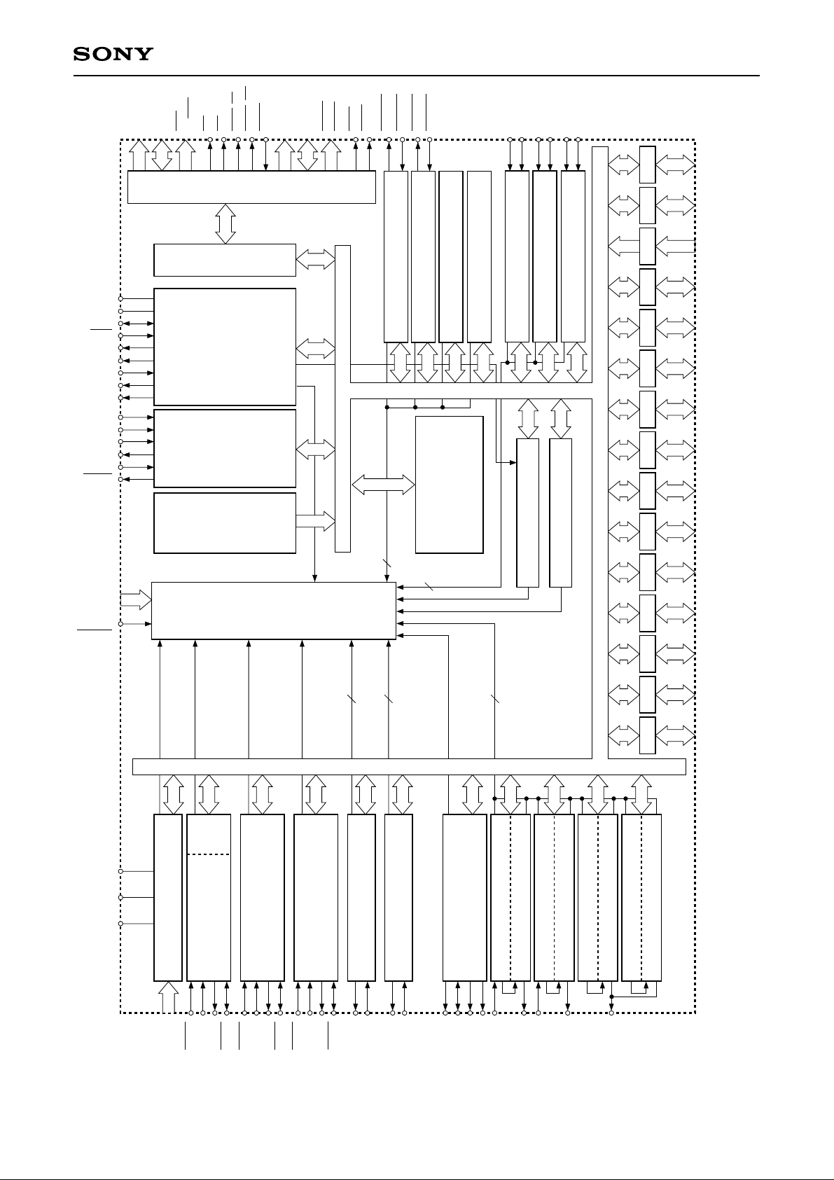
A0
to A23D0to D15
16
24
CS0
to CS7RDWE
8
LWR/LB
UWR/UB
WAIT
MA0
to MA18
19
EXTERNAL BUS
MD0
to MD7
8
MCS0,
MCS1
2
MRD
MWE
DACK0
DREQ0
DACK1
DREQ1
CT0ED0
CT0ED1
CT1ED0
CT1ED1
CT2ED0
CT2ED1
CXR702080
4
PORT O
8
PORT N
V
SS
V
DD
RST
EXTAL
XTAL
XOUT
TEX
TX
TXOUT
TDI
TMS
TCK
RTCK
TRST
TDO
to INT9
INT0
MSINS
BUS INTERFACE UNIT
DMAC (CH0)
DMAC (CH1)
DMAC (CH2)
DMAC (CH3)
16-BIT CAPTURE TIMER (CH0)
16-BIT CAPTURE TIMER (CH1)
SYSTEM CONTROLLER
16-BIT CAPTURE TIMER (CH2)
CLOCK GENERATOR/
3
PORT M
7
PORT L
8
PORT K
8
PORT J
8
CPU CORE
PORT I
ARM7TDMI
RAM
256K BYTES
16K BYTES
ROM
6
1
∗
1
∗
10
INTERRUPT CONTROLLER
3
WATCHDOG TIMER
TOKEI PRESCALER
4
PORT H
6
PORT G
6
PORT F
8
PORT E
4
PORT D
SS
REF
DD
Block Diagram
AV
AV
AV
A/D CONVERTER
4
AN0
to AN3
RAM
SERIAL INTERFACE
SI0
SCS0
SERIAL INTERFACE
UNIT (CH0)
SI1
SO0
SCK0
SCS1
UNIT (CH1)
SERIAL INTERFACE
SI2
SO1
SCK1
SCS2
2
∗
2
UART (CH0)
UNIT (CH2)
SO2
TxD0
RxD0
SCK2
2
∗
2
UART (CH1)
TxD1
RxD1
– 2 –
2
∗
MEMORY STICK INTERFACE
MSBS
MSDIO
EC0
MSIDR
MSSCLK
1
∗
8
8-BIT TIMER/COUNTER (CH0)
8-BIT TIMER (CH1)
T1
EC2
8-BIT TIMER/COUNTER (CH2)
8-BIT TIMER (CH3)
T3
8-BIT TIMER (CH4)
8-BIT TIMER (CH5)
BEEP
PORT C
PORT B
PORT A
8-BIT TIMER (CH6)
8-BIT TIMER (CH7)
6
8
6
The number of causes of interrupts generated from the module is as shown. But the number of causes input to the interrupt controller differs from the shown becauses of OR.
A part of the interrupt signals generated from UART, MEMORY STICK INTERFACE is input to the interrupt controller via DMA depending on applications.
1
2
∗
∗
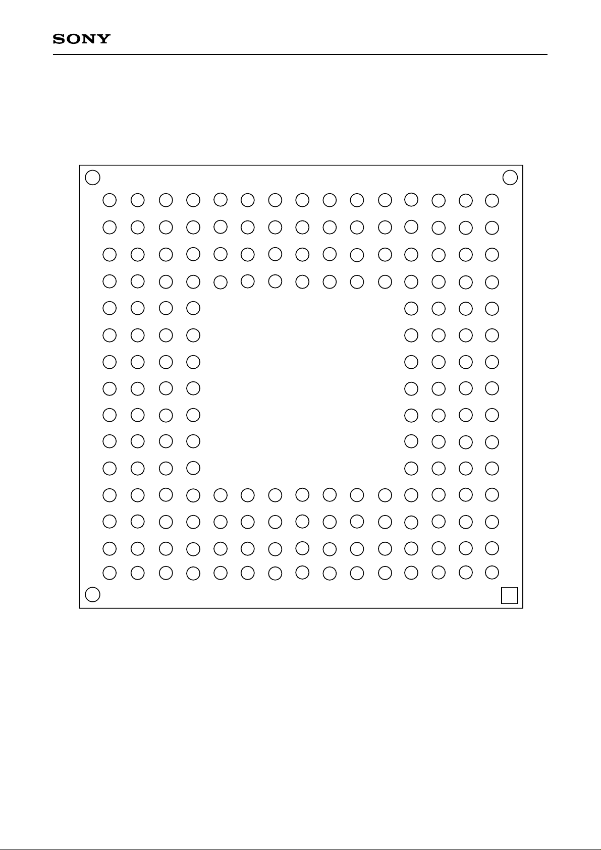
Pin Assignment (Top View) 176-pin LFLGA package
• Pin Assignment
CXR702080
23456789101112131415 1
80
78
79
75
77
72
76
74
8591
111
115
119
123
838687
818290
84
9495
102103100
106107104
110
114
118
122
R
P
N
M
L
K
J
H
G
F
E
88
89
93
97
101
105
109
113
117
121
124
92
96 99 98
108
112
116
120
68
71
70
6973
64
67
66
65
60
63
62
61
56
59
58
57
52
55
54
53
49
48
47
51
41
4050
34
35
30 2831
26
27 24
22 23
19
18
14
15
10
45
46
38
37
32
20
16
12
44
43
42
39
36
33
29
25
21
17
811
13
R
P
N
M
L
K
J
H
G
F
E
128
125
D
C
B
A
127
130
131
132
126
134
133
1415
129
135
137
138
139
136
141
142
143
140
145
146
147
144
149
150
151
148
153
154
155
152
157
158
159
156
161
162
163
160
165
166
167
164
168
6
172
169
171
173
170
174
4
3
2
175
2345678910111213
9
5
1
176
1
D
C
B
A
7
– 3 –
• Pin Assignment Table
CXR702080
Pin
No.
1
2
3
4
5
6
7
8
9
10
11
12
13
14
15
16
17
18
19
20
21
22
23
24
25
26
27
28
29
30
31
32
33
34
35
36
37
Pin
position
B1
B2
C2
D2
C1
D4
D3
E2
D1
E4
E3
F2
E1
F4
F3
G2
F1
G4
G3
H2
G1
H4
H3
J2
H1
J4
J3
K2
J1
K4
K3
L2
K1
L4
L3
L1
M2
Symbol
PB3
PB4
PB5
PB6
PB7
VDD
VSS
PC0
PC1
PC2
PC3
PC4
PC5
PD0
PD1
PD2
PD3
VDD
VSS
PE0/INT0
PE1/INT1
PE2/INT2
PE3/INT3
PE4/INT4
PE5/INT5
PE6/INT6
PE7/INT7
PF0/EC0
PF1/T1
PF2/EC2
PF3/T3
PF4/BEEP
PF5/TXOUT
VDD
VSS
PG0/CT0ED0
PG1/CT0ED1
Pin
No.
38
39
40
41
42
43
44
45
46
47
48
49
50
51
52
53
54
55
56
57
58
59
60
61
62
63
64
65
66
67
68
69
70
71
72
73
74
Pin
position
N2
M1
M3
N3
N1
P1
R1
R2
P2
P3
P4
R3
M4
N4
P5
R4
M5
N5
P6
R5
M6
N6
P7
R6
M7
N7
P8
R7
M8
N8
P9
R8
M9
N9
P10
R9
M10
Symbol
PG2/CT1ED0
PG3/CT1ED1
PG4/CT2ED0
PG5/CT2ED1
PH0/TxD0
PH1/RxD0
PH2/TxD1
PH3/RxD1
VDD
VSS
PI0/MD0
PI1/MD1
PI2/MD2
PI3/MD3
PI4/MD4
PI5/MD5
PI6/MD6
PI7/MD7
VDD
VSS
PJ0/D0
PJ1/D1
PJ2/D2
PJ3/D3
PJ4/D4
PJ5/D5
PJ6/D6
PJ7/D7
VDD
VSS
PK0/D8
PK1/D9
PK2/D10
PK3/D11
PK4/D12
PK5/D13
PK6/D14
– 4 –
Pin
No.
75
76
77
78
79
80
81
82
83
84
85
86
87
88
89
90
91
92
93
94
95
96
97
98
99
100
101
102
103
104
105
106
107
108
109
110
111
Pin
position
M11
N10
R10
P11
N11
R11
P12
P13
R12
N12
N13
R13
R14
R15
P15
P14
N14
M14
N15
M12
M13
L14
M15
L12
L13
K14
L15
K12
K13
J14
K15
J12
J13
H14
J15
H12
H13
Symbol
PK7/D15
VDD
TEX
TX
VSS
CS0
CS1
RD
LWR/LB
UWR/UB
MRD
MWE/WE
MCS0
VDD
VSS
MA0
MA1/A9
MA2/A10
MA3/A11
MA4/A12
MA5/A13
MA6/A14
MA7/A15
MA8/A16
PL0/MA9/A17
PL1/MA10/A18
PL2/MA11/A19
PL3/MA12/A20
PL4/MA13/A21
PL5/MA14/A22
PL6/MA15/A23
VDD
VSS
MA16
MA17
MA18/A0
A1
CXR702080
Pin
No.
112
113
114
115
116
117
118
119
120
121
122
123
124
125
126
127
128
129
130
131
132
133
Pin
position
G14
H15
G12
G13
F14
G15
F12
F13
E14
F15
E12
E13
E15
D14
C14
D15
D13
C13
C15
B15
A15
A14
Symbol
A2
A3
A4
A5
A6
A7
A8
VDD
EXTAL
XTAL
VSS
MSDIO
MSBS
MSSCLK
MSDIR
MSINS
DACK0
DACK1
DREQ0
DREQ1
TEST2
TEST0
Pin
No.
134
135
136
137
138
139
140
141
142
143
144
145
146
147
148
149
150
151
152
153
154
155
Pin
position
B14
B13
B12
A13
D12
C12
B11
A12
D11
C11
B10
A11
D10
C10
B9
A10
D9
C9
B8
A9
D8
C8
Symbol
TEST1
AN0
PM0/AN1
PM1/AN2
PM2/AN3
AVSS
AVREF
AVDD
TDI
TMS
TRST
TCK
RTCK
TDO
RST
VDD
VSS
PN0/SCK0
PN1/SO0
PN2/SI0
PN3/SCS0/INT8
PN4/SCK1
Pin
No.
156
157
158
159
160
161
162
163
164
165
166
167
168
169
170
171
172
173
174
175
176
Pin
position
B7
A8
D7
C7
B6
A7
D6
C6
B5
A6
D5
C5
A5
B4
B3
A4
C4
C3
A3
A2
A1
Symbol
PN5/SO1
PN6/SI1
PN7/SCS1/INT9
PO0/SCK2
PO1/SO2
PO2/SI2
PO3/SCS2
XOUT/CKO
V
DD
VSS
NC
NC
PA0/WAIT
PA1/CS2
PA2/CS3
PA3/CS4
PA4/CS5
PA5/MCS1
PB0
PB1
PB2
– 5 –
Pin Functions
CXR702080
Symbol
PA0/WAIT
PA1/CS2
to PA4/CS5
PA5/MCS1
PB0 to PB7
PC0 to PC5
PD0, PD1
PD2, PD3
I/O
I/O / Input
I/O / Output
I/O / Output
I/O
I/O
Output
I/O
Functions
(Port A)
6-bit I/O port.
Wait input for external bus
I/O can be specified in
1-bit units.
Pull-up resistor can be
Chip select output for external S bus
(4 pins)
incorporated through
program in 1-bit units.
(6 pins)
Chip select output for external M bus.
(Port B)
8-bit I/O port.
I/O can be specified in 1-bit units.
Pull-up resistor can be incorporated through program in 1-bit units.
(8 pins)
(Port C)
6-bit I/O port.
I/O can be specified in 1-bit units.
Pull-up resistor can be incorporated through program in 1-bit units.
(6 pins)
(Port D)
4-bit open drain port. Lower 2 bits are for output; upper 2 bits are for I/O.
(4mA drive)
Upper 2 bits can be specified in 1-bit units.
(4 pins)
PE0/INT0
to PE7/INT7
PF0/EC0
PF1/T1
PF2/EC2
PF3/T3
PF4/BEEP
PF5/TXOUT
PG0/CT0ED0
to PG5/
CT2ED1
I/O / Input
I/O / Input
I/O / Output
I/O / Input
I/O / Output
I/O / Output
I/O / Output
I/O / Input
(Port E)
8-bit I/O port.
I/O can be specified in
1-bit units.
Pull-up resistor can be
incorporated through
program in 1-bit units.
(8 pins)
(Port F)
6-bit I/O port.
I/O can be specified in
1-bit units.
Pull-up resistor can be
incorporated through
program in 1-bit units.
(6 pins)
(Port G)
6-bit I/O port.
I/O can be specified in
1-bit units.
Pull-up resistor can be
incorporated through
program in 1-bit units.
(6 pins)
External interruption request input.
(8 pins)
External event input to 8-bit timer (CH0).
8-bit timer (CH1) output.
External event input to 8-bit timer (CH2).
8-bit timer (CH3) output.
Beep output.
Sub oscillation output.
Capture input of 16-bit capture timer.
(6 pins)
– 6 –

CXR702080
Symbol
PH0/TxD0
PH1/RxD0
PH2/TxD1
PH3/RxD1
PI0/MD0
to PI7/MD7
PJ0/D0
to PJ7/D7
PK0/D8
to PK7/D15
I/O
I/O / Output
I/O / Input
I/O / Output
I/O / Input
I/O / I/O
I/O / I/O
I/O / I/O
(Port H)
4-bit I/O port.
I/O can be specified in
1-bit units.
Pull-up resistor can be
incorporated through
program in 1-bit units.
(4 pins)
(Port I)
8-bit I/O port.
I/O can be specified in
1-bit units.
Pull-up resistor can be
incorporated through
program in 1-bit units.
(8 pins)
(Port J)
8-bit I/O port.
I/O can be specified in
1-bit units.
Pull-up resistor can be
incorporated through
program in 1-bit units.
(8 pins)
(Port K)
8-bit I/O port.
I/O can be specified in
1-bit units.
Pull-up resistor can be
incorporated through
program in 1-bit units.
(8 pins)
Functios
UART (CH0) transmit data output.
UART (CH0) receive data input.
UART (CH1) transmit data output.
UART (CH1) receive data input.
Data bus for external M bus.
(8 pins)
Data bus for external S bus.
(16 pins)
A1 to A8
MA18/A0
MA1/A9
to MA8/A16
PL0/MA9/A17
to PL6/MA15/
A23
MA0
MA16, MA17
AN0
PM0/AN1
to PM2/AN3
Output
Output / Output
Output / Output
I/O / Output /
Output
Output
Output
Input
Input / Input
(Port L)
7-bit I/O port.
I/O can be specified in
1-bit units.
Pull-up resistor can be
incorporated through
program in 1-bit units.
(7 pins)
(Port M)
3-bit input port.
(3-pins)
– 7 –
Address bus output for
external S bus.
(24 pins)
Address bus output for
external M bus
(19 pins)
Analog input to A/D converter.
(4 pins)
CXR702080
Symbol
PN0/SCK0
PN1/SO0
PN2/SI0
PN3/SCS0/
INT8
PN4/SCK1
PN5/SO1
PN6/SI1
PN7/SCS1/
INT9
PO0/SCK2
PO1/SO2
PO2/SI2
PO3/SCS2
I/O
I/O / I/O
I/O / Output
I/O / Input
I/O / Input /
Input
I/O / I/O
I/O / Output
I/O / Input
I/O / Input /
Input
I/O / I/O
I/O / Output
I/O / Input
I/O / Input
(Port N)
8-bit I/O port.
I/O can be specified in
1-bit units.
Pull-up resistor can be
incorporated through
program in 1-bit units.
(8 pins)
(Port O)
4-bit I/O port.
I/O can be specified in
1-bit units.
Pull-up resistor can be
incorporated through
program in 1-bit units.
(4 pins)
Functios
Serial clock (CH0) I/O.
Serial data (CH0) output.
Serial data (CH0) input.
Serial chip select (CH0) External interruption
input. request input.
Serial clock (CH1) I/O.
Serial data (CH1) output.
Serial data (CH1) input.
Serial chip select (CH1) External interruption
input. request input.
Serial clock (CH2) I/O.
Serial data (CH2) output.
Serial data (CH2) input.
Serial chip select (CH2) input.
CS0, CS1
RD
LWR/LB
UWR/UB
MRD
MWE/WE
MCS0
DACK0
DREQ0
DACK1
DREQ1
MSDIR
MSBS
MSSCLK
MSDIO
Output
Output
Output / Output
Output / Output
Output
Output / Output
Output
Output
Input
Output
Input
Output
Output
Output
I/O
Chip select output for external S bus.
(2 pins)
Read signal output for external S bus.
Write strobe signal output for D0 to
D7.
Write strobe signal output for D8 to
D15.
Strobe signal output indicates
access to D0 to D7.
Strobe signal output indicates
access to D8 to D15.
Read signal output for external M bus.
Write signal output for external M bus.
Write signal output for external S bus.
Chip select output for external M bus.
Transfer request acknowledge signal output from DMA controller (CH0).
Transfer request input to DMA controller (CH0).
Transfer request acknowledge signal output from DMA controller (CH1).
Transfer request input to DMA controller (CH1).
Memory stick interface data I/O direction monitor.
Memory stick interface bus state output.
Memory stick interface clock output.
Memory stick interface data I/O direction monitor.
MSINS
TEST0
TEST1
TEST2
TDI
Input
Input
Input
Input
Input
Memory stick interface card detection.
Test. (Connect to Vss.)
Data input for JTAG boundary scanning test.
– 8 –
CXR702080
Symbol
TMS
TRST
TCK
RTCK
TDO
EXTAL
XTAL
XOUT/CKO
TEX
TX
RST
NC
AVDD
AVREF
AVSS
VDD
VSS
I/O
Input
Input
Input
Output
Output
Input
Output
Output / Output
Input
Output
I/O
Input
Functions
Test mode control input for JTAG boundary scanning test.
Reset input for JTAG boundary scanning test.
Clock input for JTAG boundary scanning test.
Clock output for JTAG boundary scanning test.
Data output for JTAG boundary scanning test.
Oscillation connector of main oscillation.
(When a clock is supplied externally, input it to EXTAL; opposite phase
clock should be input to XTAL.)
Main oscillation output.
System clock output.
Oscillation connector of main oscillation.
(When a clock is supplied externally, input it to TEX; opposite phase
clock should be input to TX.)
System reset.
NC. (Leave this pin open or connect to Vss.)
Positive power supply for A/D converter.
Reference voltage input for A/D converter.
GND for A/D converter.
Positive power supply (Connect all twelve VDD pins to positive power supply.)
GND (Connect all twelve Vss pins to GND)
– 9 –
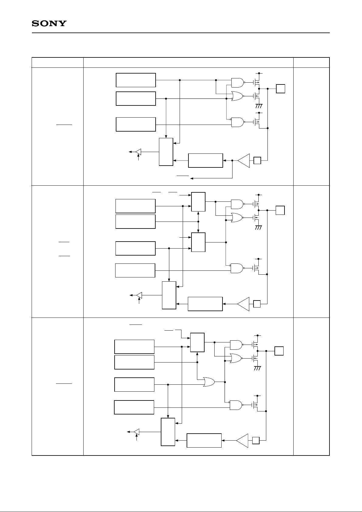
I/O Circuit Format for Pins
Pin Circuit format After a reset
CXR702080
Port A data
Port A direction
"0" after a reset
PA0/WAIT
PA1/CS2
to
PA4/CS5
Pull-up resistor
"0" after a reset
Internal data bus
Port A
function select
"0" after a reset
Port A direction
"0" after a reset
Pull-up resistor
"0" after a reset
Internal data bus
RD
Port A data
RD
MPX
CS2 to CS5
S bus pin active
MPX
WAIT
Input data
latch
MPX
MPX
Input data
latch
Hi-Z
IP
Hi-Z
IP
PA5/MCS1
Port A
function select
"0" after a reset
Port A direction
"0" after a reset
Pull-up resistor
"0" after a reset
Internal data bus
MCS1
(M bus unused: CS7)
Port A data
RD
MPX
– 10 –
MPX
Input data
latch
Hi-Z
IP
 Loading...