

Sony CXP972032, CXP973064, CXP973032 Datasheet

CMOS 16-bit Single Chip Microcomputer
Description
The CXP972032/973032/973064 is a CMOS 16-bit
microcomputer integrating on a single chip an A/D
converter, serial interface, I2C bus interface, timer,
PWM output circuit, programmable pattern
generator, remote control receive circuit, parallel
interface, as well as basic configurations like a 16-bit
CPU, ROM, RAM, and I/O port.
This LSI also provides the sleep/stop functions that
enable lower power consumption.
Features
• An efficient instruction set as a controller
— Direct addressing, numerous abbreviated forms,
multiplication and division instructions
• Instruction sets for C language and RTOS
— Highly quadratic instruction system,
general-
purpose register of 16-bit × 8-pin × 16-bank
configuration
• Minimum instruction cycle
50ns at 40MHz operation (2.7 to 3.6V)
• Incorporated ROM capacity
128K bytes (CXP972032/973032)
256K bytes (CXP973064)
• Incorporated RAM capacity
7.5K bytes (CXP972032)
11.5K bytes (CXP973032/973064)
• Peripheral functions
— A/D converter 8-bit 12-analog input, successive approximation system,
3-stage FIFO (Conversion time: 1.55µs at 40MHz)
— Serial interface Asynchronous serial interface (UART)
128-byte buffer RAM, 3 channels
— I2C bus interface 64-byte buffer RAM
(supports master/slave and automatic transfer mode)
— Timers 8-bit timer/counter, 2 channels (with timing output)
16-bit capture timer/counter (with timing output)
16-bit timer, 4 channels, watchdog timer
— PWM output circuit 14-bit PWM, 4 channels
(2 channels of binary output switch function by PPG)
— Programmable pattern generator 16-bit output, 64-byte buffer RAM, 1 channel
— Remote control receive circuit 8-bit pulse measurement counter, 10-stage FIFO
— Parallel interface External register interface (8-bit parallel bus), 4-chip select
• Interruption 33 factors, 33 vectors, multi-interruption and priority selection possible
• Standby mode Sleep/stop
• Package 100-pin plastic QFP (CXP972032/973032/973064)
100-pin plastic LQFP (CXP972032/973032/973064)
104-pin plastic LFLGA (CXP973064)
• Piggy/evaluation chip CXP971000
•
FLASH EEPROM incorporated version
CXP973F064
Structure
Silicon gate CMOS IC
– 1 –
E99930A14-PS
Sony reserves the right to change products and specifications without prior notice. This information does not convey any license by
any implication or otherwise under any patents or other right. Application circuits shown, if any, are typical examples illustrating the
operation of the devices. Sony cannot assume responsibility for any problems arising out of the use of these circuits.
CXP972032/973032/973064
100 pin QFP (Plastic) 100 pin LQFP (Plastic)
104 pin LFLGA (Plastic)
Perchase of Sony's I2C components conveys a licence under the Philips I2C Patent Rights to use these components
in an I2C system, provided that the system conforms to the I2C Standard Specifications as defined by Philips.
– 2 –
CXP972032/973032/973064
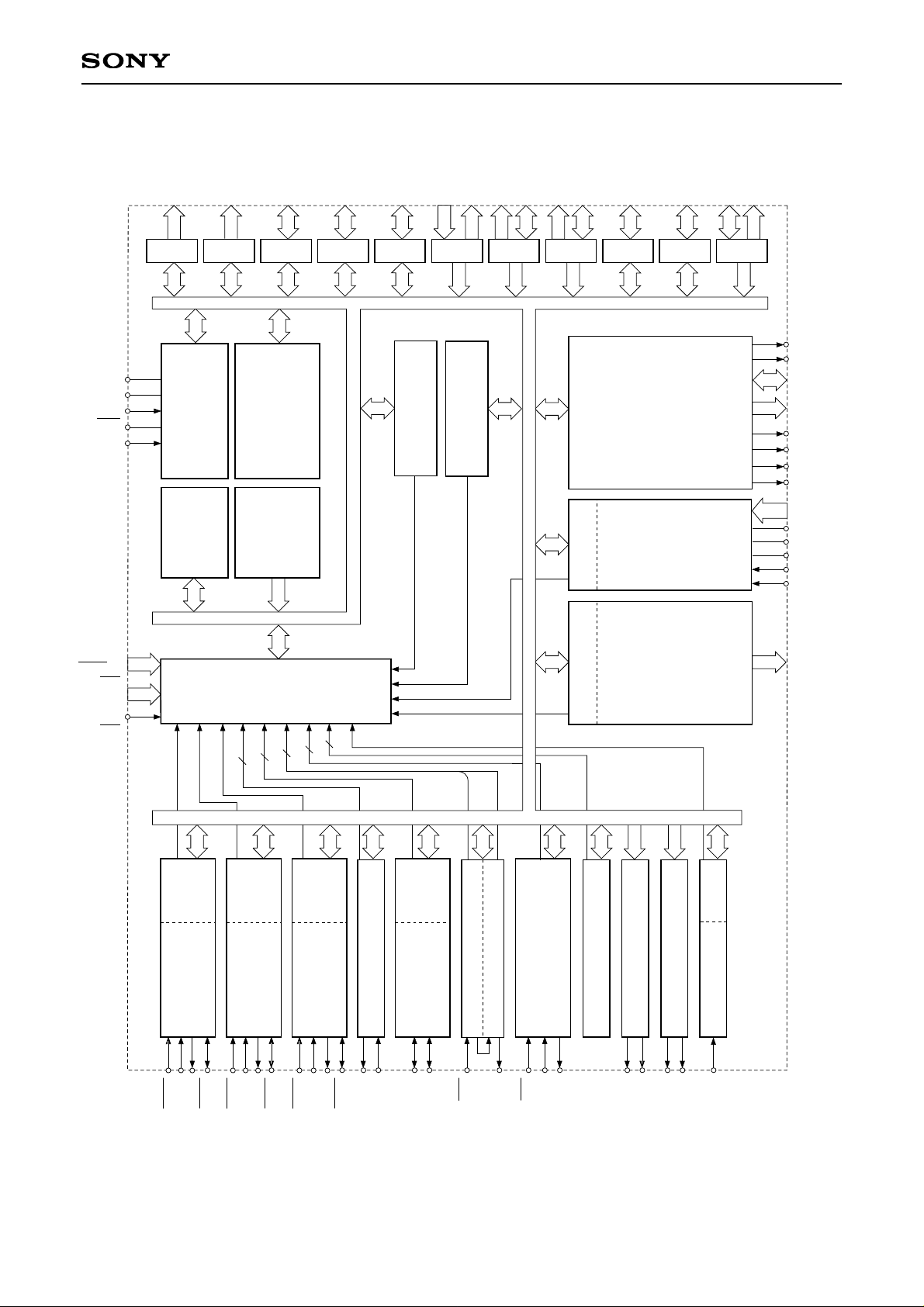
Block Diagram
PA0 to PA7
PB0 to PB7
PC0 to PC7
PD0 to PD7
PE0 to PE7
PF0 to PF5
PF6, PF7
PH0, PH1,
PH6, PH7
PI0 to PI7
PJ0 to PJ7
SCS0
SO0
SI0
SCK0
SI1
SCS1
SCK1
SO1
SCS2
SO2
SI2
SCK2
T1
PWM0
EC0
RMC
PORT A
16-BIT CAPTURE
TIMER/COUNTER (CH2)
BUFFER
RAM
I
2
C BUS
INTERFACE
UNIT
BUFFER
RAM
SERIAL
INTERFACE
UNIT (CH2)
BUFFER
RAM
SERIAL
INTERFACE
UNIT (CH1)
BUFFER
RAM
SERIAL
INTERFACE
UNIT (CH0)
8
8 20
PORT B
8
PORT C
8
PORT D
8
PG4 to PG74PH2 to PH5
4
PORT E
8
PORT F
6
2
PG0 to PG34
4
PORT G
PK0 to PK4
5
PK5 to PK62
PORT K
PORT HPORT IPORT J
8
8
SPC970
CPU CORE
CLOCK GENERAT OR/
SYSTEM CONTROLLER
ROM
128K/256K
BYTES
RAM
7.5K/11.5K
BYTES
PWM1
PWM2
PWM3
T2
PRESCALER/
TIME-BASE TIMER
EC2
CINT
SCL
SDA
TxD
RxD
INT0
to INT7
KS0
to KS19
NMI
RST
EXTAL
XTAL
V
DD
VSS
16
A/D
CONVERTER
12
8
REMOCON
FIFO
2CH 14-BIT PWM (PPG)
2CH 14-BIT PWM
4CH 16-BIT TIMER
UART
INTERRUPT CONTROLLER
AN0
to AN11
PPO00
to PPO15
16
D0 to D7
A0 to A15
ADTEN
ADTRG
XCS3
XCS2
XCS1
XCS0
XRD
XWR
AVSS
AVREF
AVDD
8-BIT TIMER/COUNTER (CH0)
8-BIT TIMER (CH1)
2
4
2
3
2
PROGRAMABLE
PATTEERN
GENERATOR
EXT. REGISTERS
INTERFACE
BUFFER RAM FIFO
TOKEI PRESCALER
– 3 –
CXP972032/973032/973064
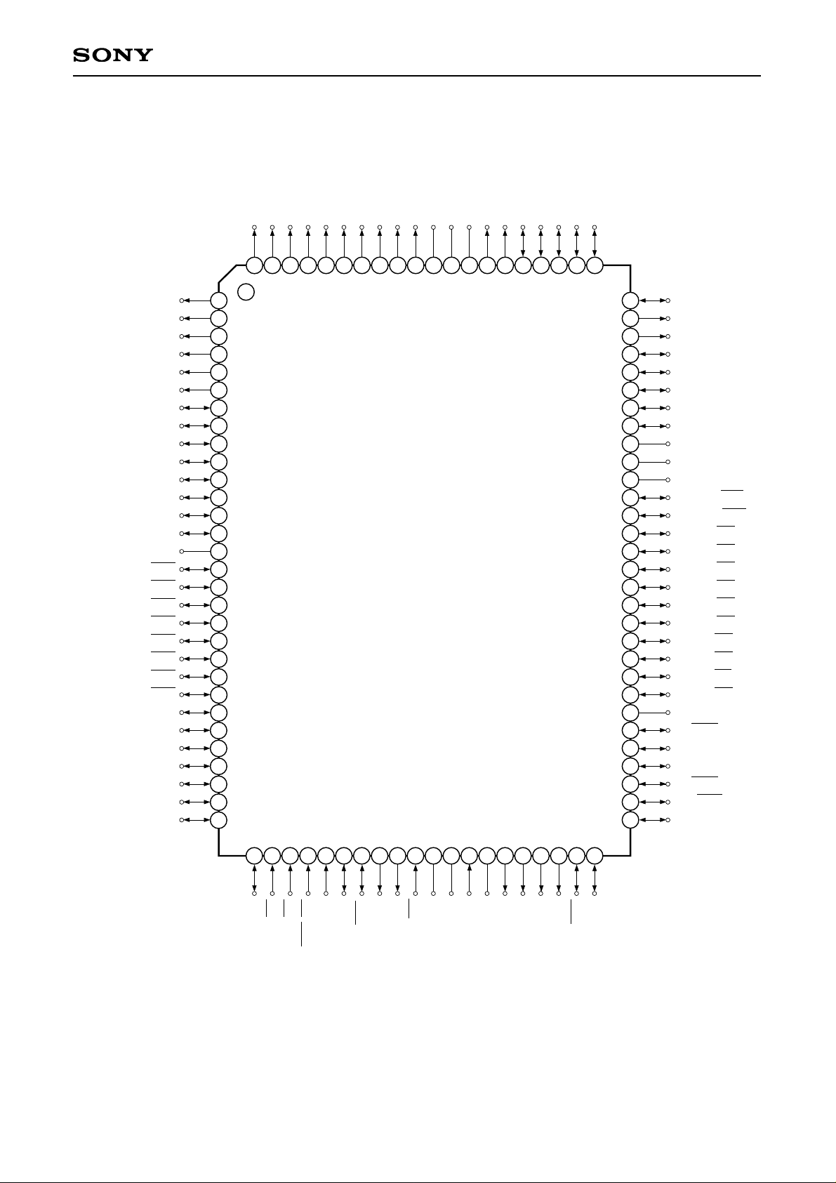
Pin Assignment 1 (Top View) 100-pin QFP package
31 32 33 34 35 36 37 38 39 404142 43 44 45
46
47
48 49 50
57
58
59
60
61
62
63
64
65
66
67
68
69
70
71
72
73
74
75
76
77
78
79
80
81828384858687888990919293949596979899
1
2
3
4
5
6
7
8
9
10
11
12
13
14
15
16
17
18
19
20
21
22
23
24
PE7/INT7/CINT
PF0/EC0
PF1/EC2
PF2/SCS1/NMI
PF3/SI1
PF4/SO1
PF5/SCK1
PF6/T1
PF7/T2
RST
V
SS
XTAL
EXTAL
V
DD
PG0/PWM0
PG1/PWM1
PG2/PWM2
PG3/PWM3
PG4/SCS0
PG5/SI0
PH0/SDA
PK6
PK5
PK4/ADTRG
PK3/ADTEN
PK2
PK1
PK0
AV
DD
AVREF
AVSS
PJ7/AN11/KS11
PJ6/AN10/KS10
PJ5/AN9/KS9
PJ4/AN8/KS8
PJ3/AN7/KS7
PJ2/AN6/KS6
PJ1/AN5/KS5
PJ0/AN4/KS4
PI7/AN3/KS3
PI6/AN2/KS2
PI5/AN1/KS1
PI4/AN0/KS0
Vss
PI3/SCK2
51
52
53
54
55
56
PI2/SO2
PI1/SI2
PI0/SCS2
PG7/SCK0
PG6/SO0
PB2/PPO02/A10
PB3/PPO03/A11
PB4/PPO04/A12
PB5/PPO05/A13
PB6/PPO06/A14
PB7/PPO07/A15
PC0/PPO08
PC1/PPO09
PC2/PPO10
PC3/PPO11
PC4/PPO12/XCS3
PC5/PPO13/XCS2
PC6/PPO14/XCS1
PC7/PPO15/XCS0
V
SS
PD0/D0/KS12
PD1/D1/KS13
PD2/D2/KS14
PD3/D3/KS15
PD4/D4/KS16
PD5/D5/KS17
PD6/D6/KS18
PD7/D7/KS19
PE0/INT0
25
26
27
28
29
PE1/INT1
PE2/INT2
PE3/INT3
PE4/INT4
PE5/INT5
30
PE6/INT6
PB1/PPO01/A9
PB0/PPO00/A8
PA7/A7
PA6/A6
PA5/A5
PA4/A4
PA3/A3
PA2/A2
PA1/A1
PA0/A0
VSSVDDNCPH7/XRD
PH6/XWR
PH5
PH4/RMC
PH3/TxD
PH2/RxD
PH1/SCL
100
Note) 1. NC (Pin 88) must be left open. However, use this pin for FLASH EEPROM
incorporated version.
2. Vss and AVss (Pins 15, 41, 57, 70 and 90) must be connected to GND.
3. VDD and AVDD (Pins 44, 72 and 89) must be connected to VDD.
– 4 –
CXP972032/973032/973064
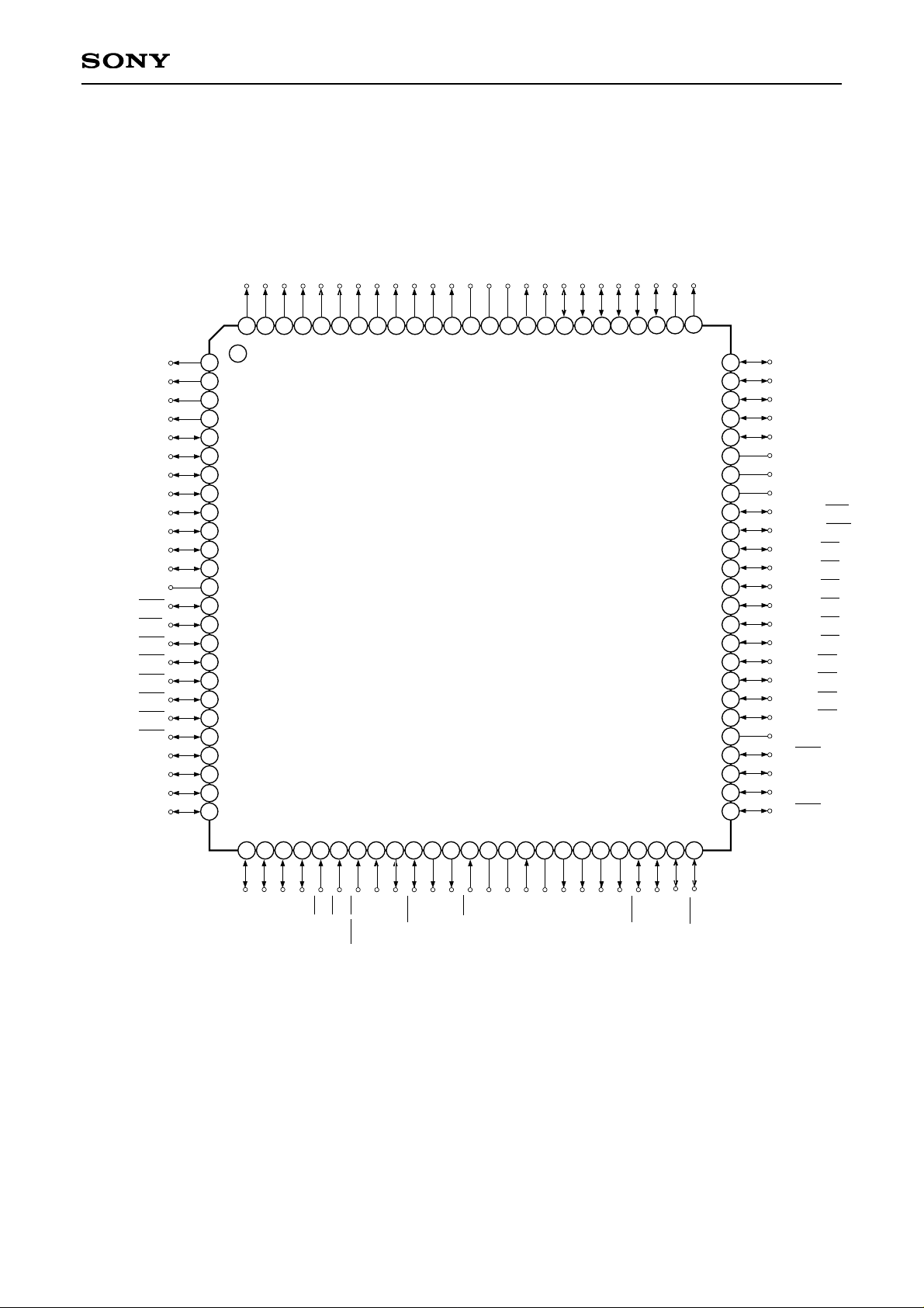
Pin Assignment 2 (Top View) 100-pin LQFP package
31 32 33 34 35 36 37 38 39 404142 43 44 45
46
47
48 49 50
57
58
59
60
61
62
63
64
65
66
67
68
69
70
71
72
73
74
75
76
77
78
79
80
81828384858687888990919293949596979899
1
2
3
4
5
6
7
8
9
10
11
12
13
14
15
16
17
18
19
20
21
22
23
24
PE7/INT7/CINT
PF0/EC0
PF1/EC2
PF2/SCS1/NMI
PF3/SI1
PF4/SO1
PF5/SCK1
PF6/T1
PF7/T2
RST
V
SS
XTAL
EXTAL
V
DD
PG0/PWM0
PG1/PWM1
PG2/PWM2
PG3/PWM3
PG4/SCS0
PG5/SI0
PH0/SDA
PK6
PK5
PK4/ADTRG
PK3/ADTEN
PK2
PK1
PK0
AV
DD
AVREF
AVSS
PJ7/AN11/KS11
PJ6/AN10/KS10
PJ5/AN9/KS9
PJ4/AN8/KS8
PJ3/AN7/KS7
PJ2/AN6/KS6
PJ1/AN5/KS5
PJ0/AN4/KS4
PI7/AN3/KS3
PI6/AN2/KS2
PI5/AN1/KS1
PI4/AN0/KS0
Vss
PI3/SCK2
51
52
53
54
55
56
PI2/SO2
PI1/SI2
PI0/SCS2
PB4/PPO04/A12
PB5/PPO05/A13
PB6/PPO06/A14
PB7/PPO07/A15
PC0/PPO08
PC1/PPO09
PC2/PPO10
PC3/PPO11
PC4/PPO12/XCS3
PC5/PPO13/XCS2
PC6/PPO14/XCS1
PC7/PPO15/XCS0
V
SS
PD0/D0/KS12
PD1/D1/KS13
PD2/D2/KS14
PD3/D3/KS15
PD4/D4/KS16
PD5/D5/KS17
PD6/D6/KS18
PD7/D7/KS19
PE0/INT0
25
26
27 28 29
PE1/INT1
PE2/INT2
PE3/INT3
30
PE4/INT4
PE5/INT5
PE6/INT6
PB1/PPO01/A9
PB2/PPO02/A10
PB3/PPO03/A11
PB0/PPO00/A8
PA7/A7
PA6/A6
PA5/A5
PA4/A4
PA3/A3
PA2/A2
PA1/A1
PA0/A0
V
SS
VDDNCPH7/XRD
PH6/XWR
PH5
PH4/RMC
PH3/TxD
PH2/RxD
PH1/SCL
100
PG7/SCK0
PG6/SO0
Note) 1. NC (Pin 86) must be left open. However, use this pin for FLASH EEPROM
incorporated version.
2. Vss and AVss (Pins 13, 39, 55, 68 and 88) must be connected to GND.
3. VDD and AVDD (Pins 42, 70 and 87) must be connected to VDD.
– 5 –
CXP972032/973032/973064
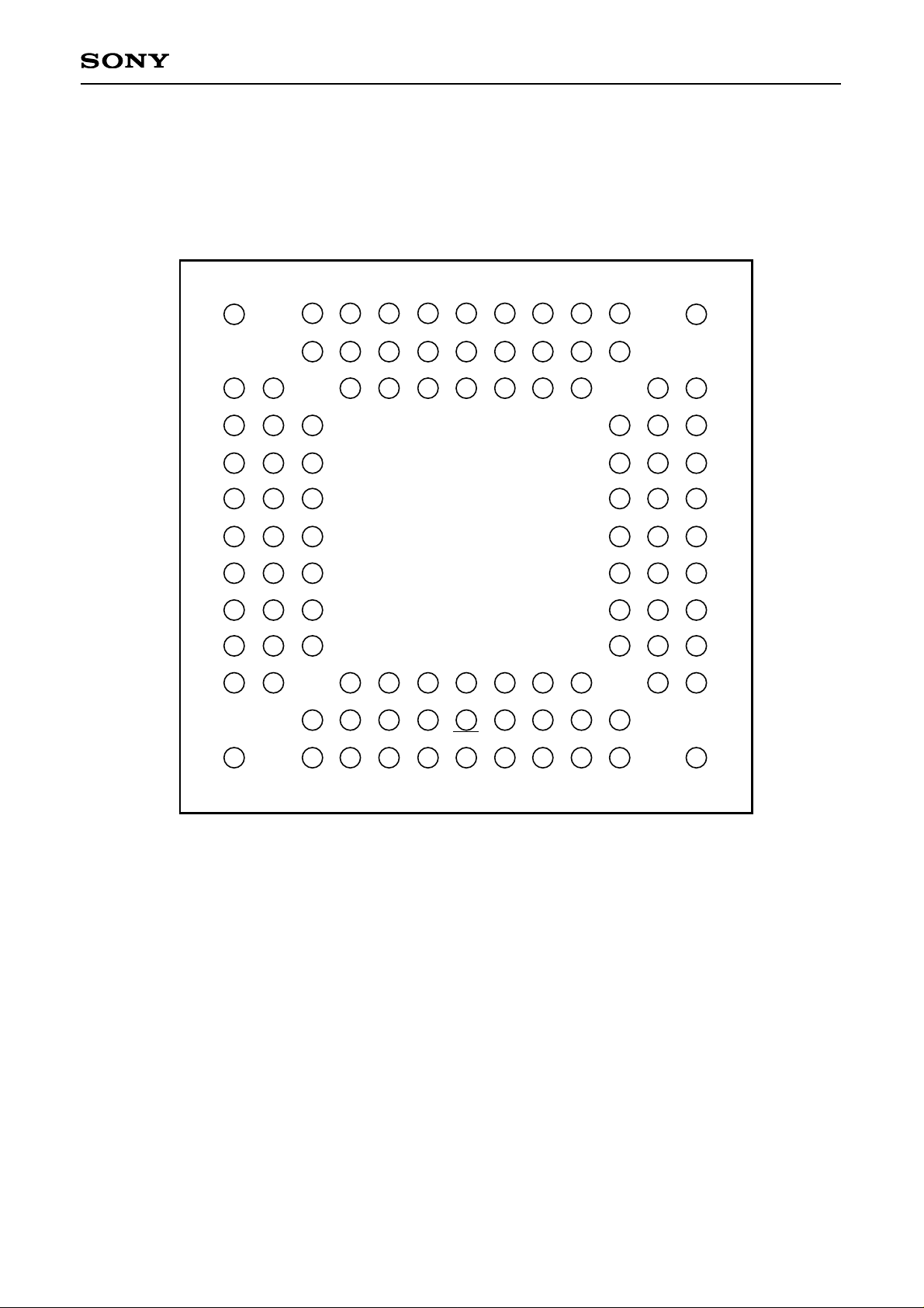
Pin Assignment 3 (Top View) 104-pin LFLGA package
3
100
2
1
5
4
6
7
8
9
10
13
12 11
15
16
14
17
18 19
20
21
22 24
23
28
25
27
26
29
30
32
31
33
353438
373639
40
41
42
43
46
444547
49
48
53
50 52
51 55
54 56 57
58 60 59
61 6263
646566
676871
6970
7274
73
78
75
77
76
80
79
81
82
83
85
84
88
87
86
90
91
89
92
93
94
95
96
97
99
98
12345678910111213
PB0 PA6 PA3 PA1 V
DD PH6 PH4 PH2 PK6
A
PB2 PA7 PA4 PA2 VSS PH7 PH3 PK5 PK4
B
PB5 PB3 PB1 PA5 PA0 NC PH5 PH1 PH0 PK3 PK1
C
PC0 PB4 PB6 PK2 AVDD AVREF
D
PC2 PC1 PB7 PK0 AV
SS PJ7
E
PC5 PC4 PC3 PJ6 PJ5 PJ4
F
PC7 V
SS PC6 PJ3 PJ1 PJ2
G
PD1 PD2 PD0 PI6 PJ0 PI7
H
PD3 PD4 PD5 PI3 PI4 PI5
J
PD6 PD7 PE1 PI2 PI0 VSS
K
PE0 PE2 PE6 PF0 PF3 PF6 EXTAL PG3 PG5 PG7 PI1
L
PE3 PE4 PF2 PF5 RST XTAL PG0 PG2 PG6
M
PE5 PE7 PF1 PF4
PF7
VSS VDD PG1 PG4
N
Note) 1. NC (Pin C7) must be left open. However, use this pin for FLASH EEPROM
incorporated version.
2. Vss and AVss (Pins B7, E12, G2, K13 and N8) must be connected to GND.
3. VDD and AVDD (Pins A7, D12 and N9) must be connected to VDD.
– 6 –
CXP972032/973032/973064
Pin Functions
Symbol
I/O
Functions
PA0/A0
to PA7/A7
PB0/PPO00/
A8
to PB7/PPO07/
A15
PC0/PPO08
to PC3/PPO11
PC4/PPO12/
XCS3
to PC7/PPO15/
XCS0
PD0/D0/
KS12
to PD7/D7/
KS19
PE0/INT0
to PE6/INT6
PE7/INT7/
CINT
PF0/EC0
PF1/EC2
PF2/SCS1/
NMI
PF3/SI1
PF4/SO1
PF5/SCK1
PF6/T1
PF7/T2
PG0/PWM0
to PG1/PWM1
PG2/PWM2
PG3/PWM3
PG4/SCS0
PG5/SI0
PG6/SO0
PG7/SCK0
Output / Output
Output /
Output / Output
I/O / Output
I/O / Output /
Output
I/O / I/O / Input
I/O / Input
I/O / Input /
Input
Input / Input
Input / Input /
Input
Input / Input
Input / Output
Input / I/O
Output / Output
Output / Output
Output / Output
Output / Output
I/O / Input
I/O / Input
I/O / Output
I/O / I/O
(Port A)
8-bit output port.
(8 pins)
(Port B)
8-bit output port. PPO
value and OR output.
(8 pins)
(Port C)
8-bit I/O port. I/O can
be specified in 1-bit
units. PPO value and
OR output.
(8 pins)
(Port D)
8-bit I/O port. I/O can
be specified in 1-bit
units.
(8 pins)
(Port E)
8-bit I/O port. I/O can
be specified in 1-bit
units. (8 pins)
External register interface address bus port
output data value and OR output.
(8 pins)
Programmable pattern generator outputs.
(16 pins)
External register
interface data bus.
(8 pins)
External interrupt inputs.
(8 pins)
External event inputs for 8-bit timer/counter.
(2 pins)
Serial chip select
(CH1) input.
Serial data (CH1) input.
Serial data (CH1) output.
Serial clock (CH1) I/O.
8-bit timer/counter output.
16-bit capture timer/counter timing output.
14-bit PWM output with output value switch
control by programmable pattern generator.
(2 pins)
14-bit PWM output.
(2 pins)
Serial chip select (CH0) input.
Serial data (CH0) input.
Serial data (CH0) output.
Serial clock (CH0) I/O.
External register interface address bus.
Address width can be extended in 1-bit
units.
(8 pins)
External register interface chip select
signal. Chip select signal output function
can be selected in 1-bit units.
(4 pins)
External capture input for 16-bit capture
timer/counter.
Standby release input
function can be
specified in 1-bit units.
(8 pins)
Non-maskable external
interrupt input.
(Port F)
8-bit port. Lower 6 bits
are for input; upper 2
bits are for output.
(8 pins)
(Port G)
8-bit port. Lower 4 bits
are for output; upper 4
bits are for I/O. Upper
4 bits can be specified
in 1-bit units.
(8 pins)
– 7 –
CXP972032/973032/973064
PH0/SDA
PH1/SCL
PH2/RxD
PH3/TxD
PH4/RMC
PH5
PH6/XWR
PH7/XRD
PI0/SCS2
PI1/SI2
PI2/SO2
PI3/SCK2
PI4/AN0/
KS0
to PI7/AN3/
KS3
PJ0/AN4/
KS4
to PJ7/AN11/
KS11
PK0 to PK2
PK3/ADTEN
PK4/ADTRG
PK5
PK6
EXTAL
XTAL
RST
AVDD
AVREF
AVss
VDD
Vss
NC
Output / I/O
Output / I/O
I/O / Input
I/O / Output
I/O / Input
I/O
Output / Output
Output / Output
I/O / Input
I/O / Input
I/O / Output
I/O / I/O
I/O / Input /
Input
I/O / Input /
Input
I/O
I/O / Input
I/O / Input
Output
Input
Input
Input
(Port I)
8-bit I/O port. I/O can
be specified in 1-bit
units.
(8 pins)
(Port J)
8-bit I/O port. I/O can
be specified in 1-bit
units.
(8 pins)
(Port K)
7-bit port. Lower 5 bits
are for I/O; upper 2 bits
are for output. Lower
5 bits can be specified
in 1-bit units.
(7 pins)
Connects a crystal for main clock oscillation. (When the clock is supplied
externally, input it to EXTAL and input an opposite phase clock to XTAL.)
System reset. Active at "L" level.
Positive power supply for A/D converter. (Must be the same voltage with
VDD)
Reference voltage input for A/D converter. (Must be the same voltage with
VDD)
GND for A/D converter.
Positive power supply.
(Connect both V
DD pins to positive power supply.)
GND. (Connect all four Vss pins to GND.)
NC. (NC is used for FLASH EEPROM incorporated version.)
I
2
C bus interface data I/O.
I2C bus interface clock I/O.
UART reception data input.
UART transmission data output.
Remote control receive circuit input.
External register interface write signal.
External register interface read signal.
Serial chip select (CH2) input.
Serial data (CH2) input.
Serial data (CH2) output.
Serial clock (CH2) I/O.
Analog input for
A/D converter.
(12 pins)
A/D converter operation enable input by external
trigger.
External trigger input for A/D converter.
Standby release input
function can be
specified in 1-bit units.
(12 pins)
Symbol
I/O
Functions
(Port H)
8-bit port. Lower 2 bits
are for large current
N-ch open drain
outputs; medium 4 bits
are for I/O; upper 2 bits
are for output. Medium
4 bits can be specified
in 1-bit units.
(8 pins)
– 8 –
CXP972032/973032/973064
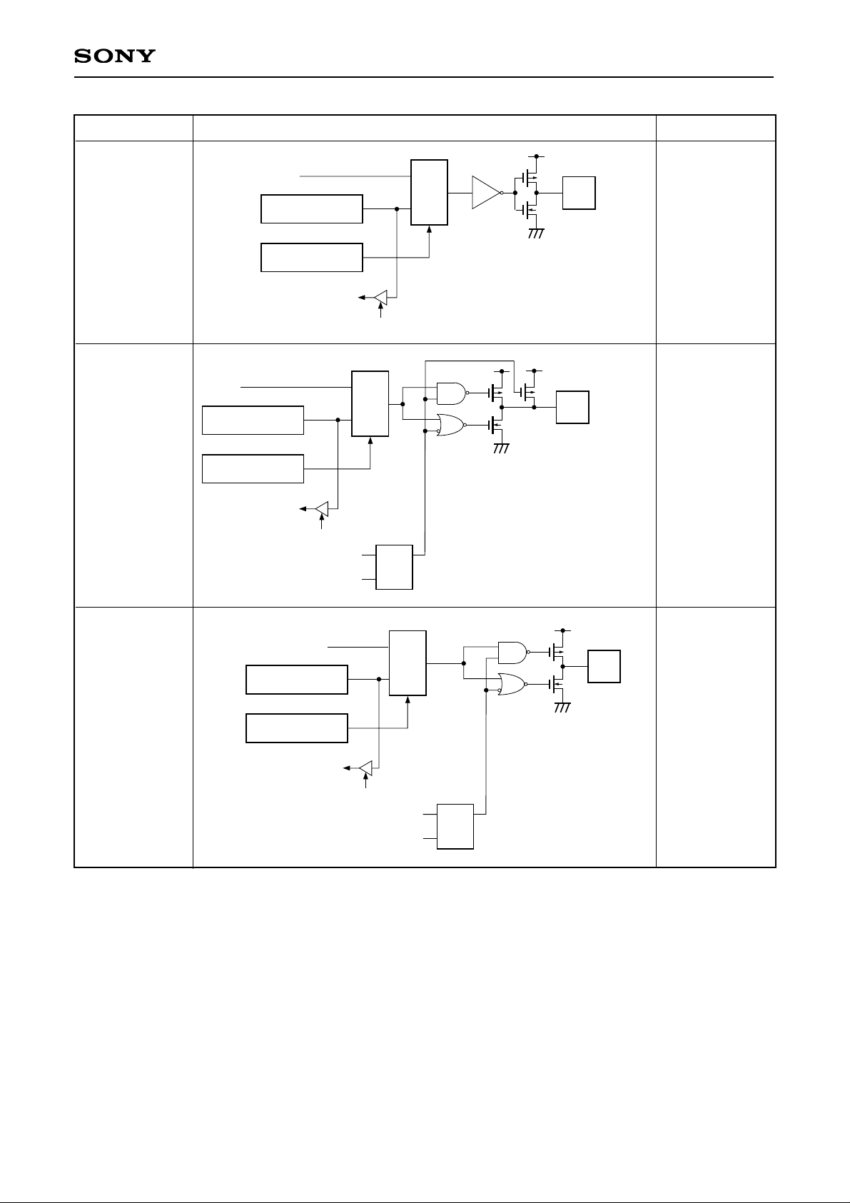
I/O Circuit Format for Pins
Pin Circuit format After a reset
PA0/A0
to PA7/A7
Hi-Z
PB0/PPO00/A8
to PB7/PPO07/
A15
Hi-Z
PC0/PPO08
to PC3/PPO11
Hi-Z
A0 to A7
RD
PA register
PA register write
(Undefined after a reset)
Reset
Internal
data bus
QS
R
A8 to A15
PPO00 to PPO07
RD
PB register
PB register write
Address width
setting
(Undefined after a reset)
("0" after a reset)
Reset
Internal
data bus
QS
R
1
MPX
0
PPO08 to PPO11
RD
PC register
Input
protection
circuit
("0" after a reset)
Internal
data bus
PCD register
("0" after a reset)
IP
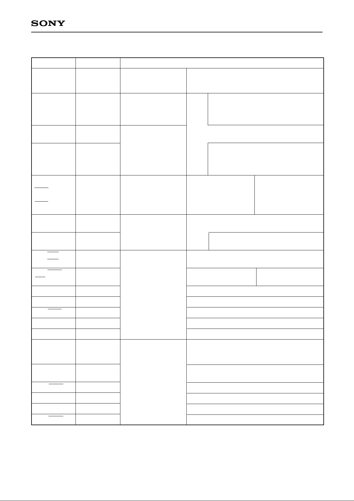
– 9 –
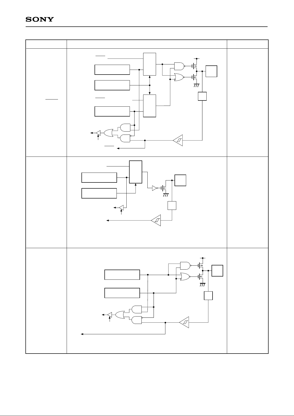
CXP972032/973032/973064
PC4/PPO12/
XCS3
to PC7/PPO15/
XCS0
Hi-Z
PD0/D0/KS12
to PD7/D7/
KS19
Hi-Z
PE0/INT0
to PE7/INT7/
CINT
Hi-Z
XCS3 to XCS0
PPO12 to PPO15
XCS output setting
1
MPX
0
RD
PC register
PCD register
Internal
data bus
("0" after a reset)
("0" after a reset)
("0" after a reset)
IP
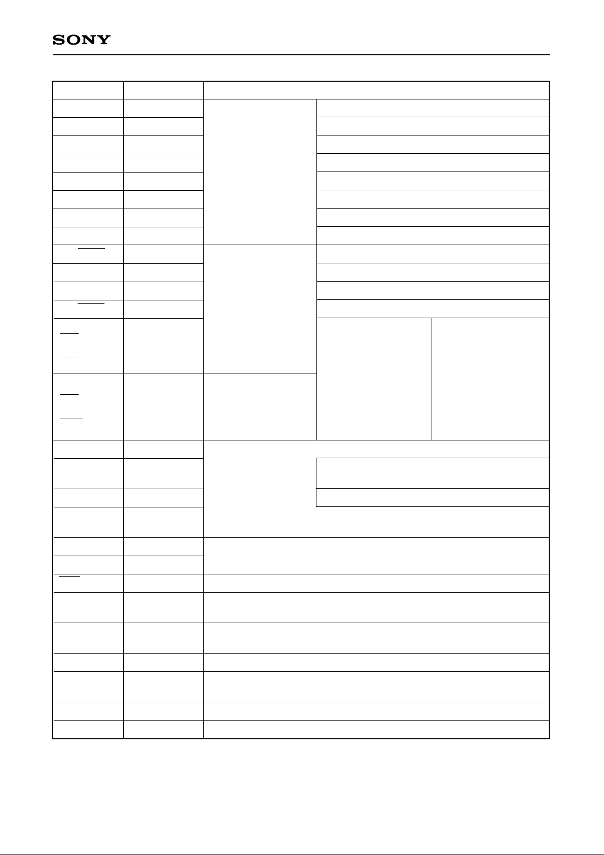
RD
PD register
PDD register
External register
I/F
External register
I/F
WR (external register area)
Internal data bus
Internal data bus
Internal data bus
External register operation enable
Standby release
("0" after a reset)
("0" after a reset)
RD (external register area)
External register operation enable
IP
CLR
CLR
∗
Large current drive
5mA (VDD = 2.7 to 3.6V)
∗
RD
PE register
PED register
Internal data bus
INT0 to INT7/CINT
(Undefined after a reset)
("0" after a reset)
CMOS Schmitt input
IP
Pin Circuit format After a reset

– 10 –
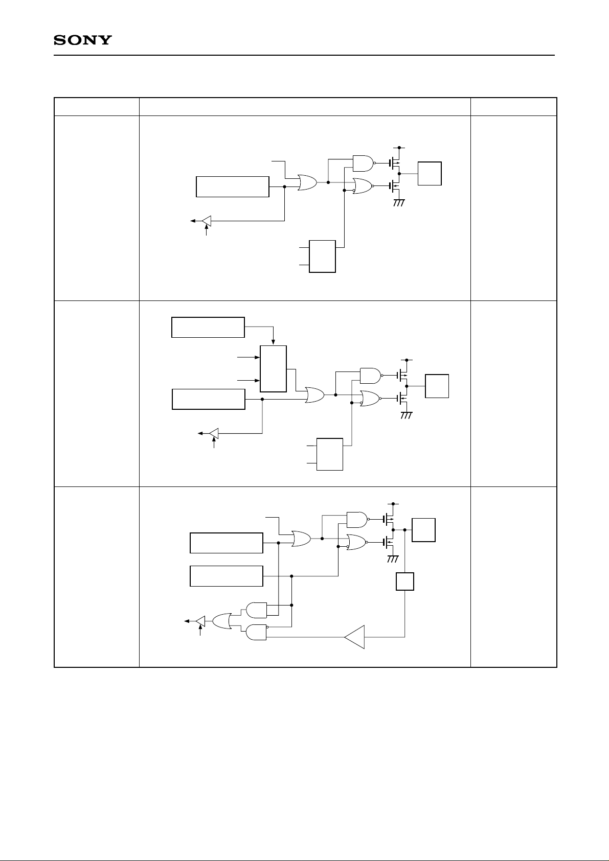
CXP972032/973032/973064
PF0/EC0
PF1/EC2
Hi-Z
PF2/SCS1/
NMI
Hi-Z
PF3/SI1
Hi-Z
PF4/SO1
Hi-Z
PF5/SCK1
Hi-Z
Internal data bus
EC0, EC2
RD
CMOS Schmitt input
IP
PFSL register
("0" after a reset)
NMI input enable
("0" after a reset)
Internal data bus
RD
CMOS Schmitt input
SCS1
NMI
IP
PFSL register
("0" after a reset)
Internal data bus
RD
CMOS Schmitt input
SI1
IP
RD
PFSL register
("0" after a reset)
SO1 output enable
SO1
Internal data bus
IP
RD
CMOS Schmitt input
PFSL register
("0" after a reset)
SCK1 output enable
SCK1
Internal data bus
IP
SCK1
Pin Circuit format After a reset
– 11 –
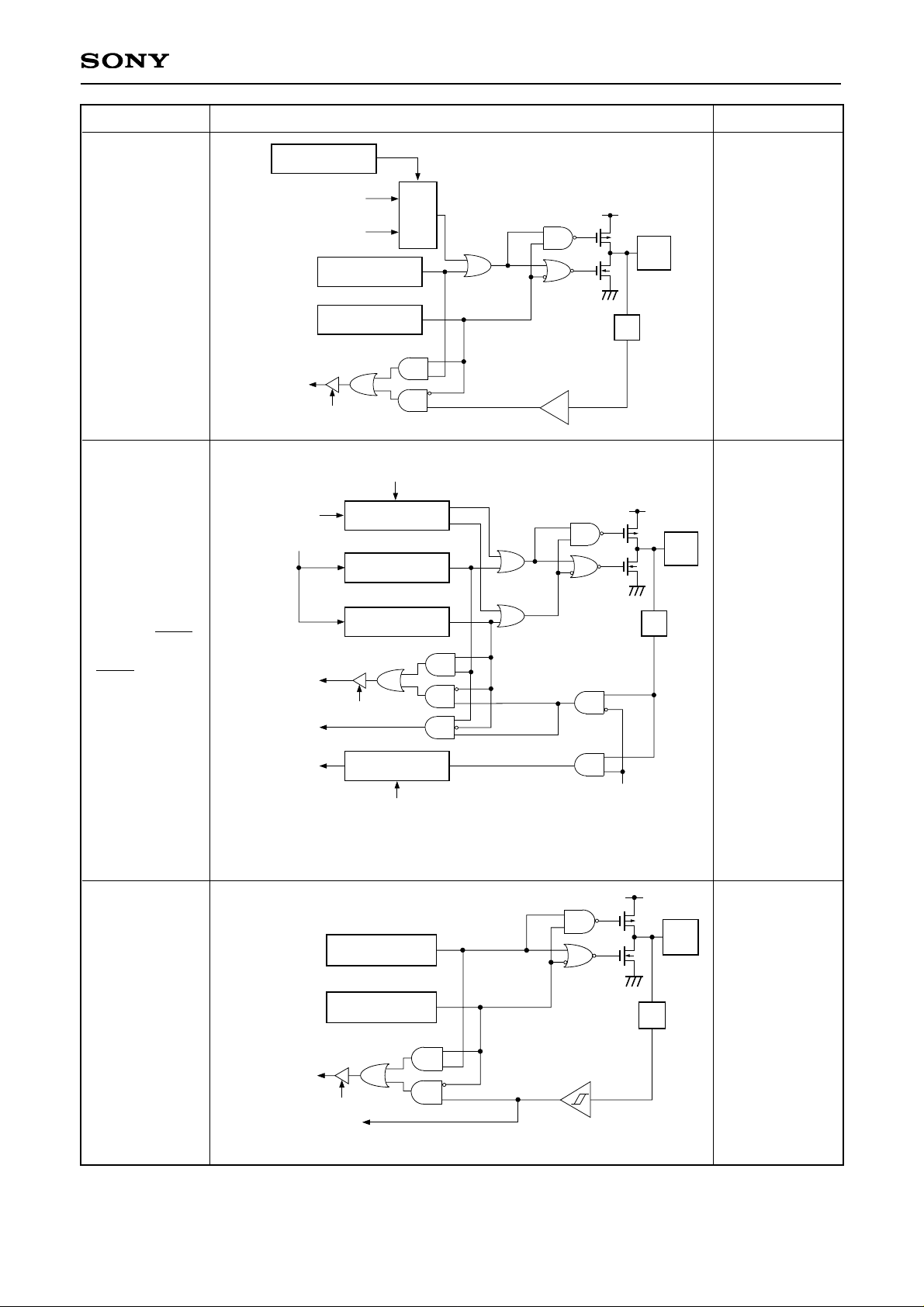
CXP972032/973032/973064
PF6/T1
"H" level
PF7/T2
"H" level
("H" level at ON
resistance of
pull-up transistor
by a reset.)
PG0/PWM0
to PG3/PWM3
Hi-Z
T1
RD
PFSL register
("1" after a reset)
("0" after a reset)
Internal data bus
1
0
MPX
PF register
PF register write
Reset
QS
R
T2
RD
PFSL register
("1" after a reset)
("0" after a reset)
Internal data bus
1
0
MPX
PF register
∗
∗
Pull-up transistor
approximately 150kΩ (VDD = 2.7 to 3.6V)
PG register write
Reset
QS
R
PWM0 to PWM3
RD
PGSL register
(Undefined after a reset)
("0" after a reset)
Internal data bus
1
0
MPX
PG register
Pin Circuit format After a reset

– 12 –
CXP972032/973032/973064
PG4/SCS0
Hi-Z
PG5/SI0
Hi-Z
PG6/SO0
Hi-Z
RD
PGD register
PGSL register
Internal data bus
SCS0
("0" after a reset)
PG register
(Undefined after a reset)
("0" after a reset)
IP
CMOS Schmitt input
RD
PGD register
PGSL register
Internal data bus
SI0
("0" after a reset)
PG register
(Undefined after a reset)
("0" after a reset)
IP
CMOS Schmitt input
RD
PG register
PGSL register
Internal
data bus
(Undefined after a reset)
("0" after a reset)
PGD register
("0" after a reset)
SO0 output enable
SO0
IP
1
MPX
0
1
MPX
0
Pin Circuit format After a reset
– 13 –
CXP972032/973032/973064
PG7/SCK0
Hi-Z
PH0/SDA
PH1/SCL
Hi-Z
PH2/RxD
Hi-Z
RD
PG register
PGSL register
Internal
data bus
(Undefined after a reset)
("0" after a reset)
PGD register
("0" after a reset)
SCK0 output enable
CMOS Schmitt input
SCK0
SCK0
IP
1
MPX
0
1
MPX
0
CMOS Schmitt input
RD
PHSL register
Internal data bus
("0" after a reset)
PH register
("1" after a reset)
SDA, SCL
SDA, SCL
IP
1
MPX
0
∗
Large current drive
5mA (VDD = 2.7 to 3.6V)
∗
CMOS Schmitt input
RD
PHL register
PHD register
Internal data bus
RxD
(Undefined after a reset)
("0" after a reset)
IP
Pin Circuit format After a reset

– 14 –
CXP972032/973032/973064
PH3/TxD
Hi-Z
PH4/RMC
Hi-Z
PH5
Hi-Z
PH6/XWR
PH7/XRD
Hi-Z
RD
PH register
Internal
data bus
(Undefined after a reset)
PHD register
("0" after a reset)
TxD output enable
TxD
IP
1
MPX
0
CMOS Schmitt input
RD
PH register
PHD register
Internal data bus
RMC
(Undefined after a reset)
("0" after a reset)
IP
CMOS Schmitt input
RD
PH register
PHD register
Internal data bus
(Undefined after a reset)
("0" after a reset)
IP
XWR, XRD
RD
PH register
PH register write
PHSL register
(Undefined after a reset)
("0" after a reset)
Reset
Internal
data bus
QS
R
1
MPX
0
Pin Circuit format After a reset
 Loading...