

Sony CXP971000 Datasheet
CMOS 16-bit Single Chip Microcomputer
Description
The CXP971000 is a CMOS 16-bit single chip
microcomputer of piggyback/evaluator combined
type, which is developed for evaluating the function
of the CXP972032/973032/973064.
Features
• An efficient instruction set as a controller
– Direct addressing, numerous abbreviated forms,
multiplication and division instructions
• Instruction sets for C language and RTOS
– Highly quadratic instruction system,
general-purpose register of eight 16-bit × 16-bank configuration
• Minimum instruction cycle time 50ns at 40MHz operation (2.7 to 3.6V)
• Incorporated EPROM CXP27V1000K
• Incorporated RAM capacity 23.5K bytes
• Peripheral functions
— A/D converter 8-bit 12-analog input, successive approximation system,
3-stage FIFO (Conversion time: 1.55µs at 40MHz)
— Serial interface Asynchronous serial interface (UART)
128-byte buffer RAM, 3 channels
— I2C bus interface 64-byte buffer RAM
(supports master/slave and automatic transfer mode)
— Timers 8-bit timer/counter, 2 channels (with timing output)
16-bit capture timer/counter (with timing output)
16-bit timer, 4 channels, watchdog timer
— PWM output circuit 14-bit PWM, 4 channels
(2-channel of binary output switch function by PPG)
— Programmable pattern generator 16-bit output, 64-byte buffer RAM, 1 channel
— Remote control receive circuit 8-bit pulse measurement counter, 10-stage FIFO
— Parallel interface External register interface (8-bit parallel bus), 4-chip select
• Interruption 33 factors, 33 vectors, multi-interruption and priority selection possible
• Standby mode Sleep/stop
• Package 100-pin Ceramic PQFP
• Mask ROM CXP972032/973032/973064
•
FLASH EEPROM incorporated type
CXP973F064
Structure
Silicon gate CMOS IC
– 1 –
E00423A08-PS
Sony reserves the right to change products and specifications without prior notice. This information does not convey any license by
any implication or otherwise under any patents or other right. Application circuits shown, if any, are typical examples illustrating the
operation of the devices. Sony cannot assume responsibility for any problems arising out of the use of these circuits.
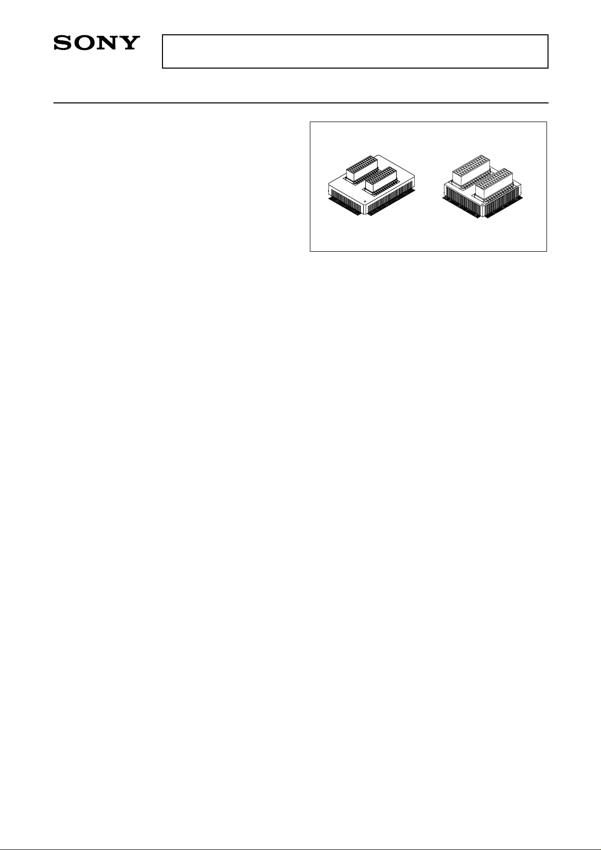
CXP971000
100 pin PQFP (Ceramic)
Piggy/
evaluation type
(QFP supported)
(LQFP supported)
– 2 –
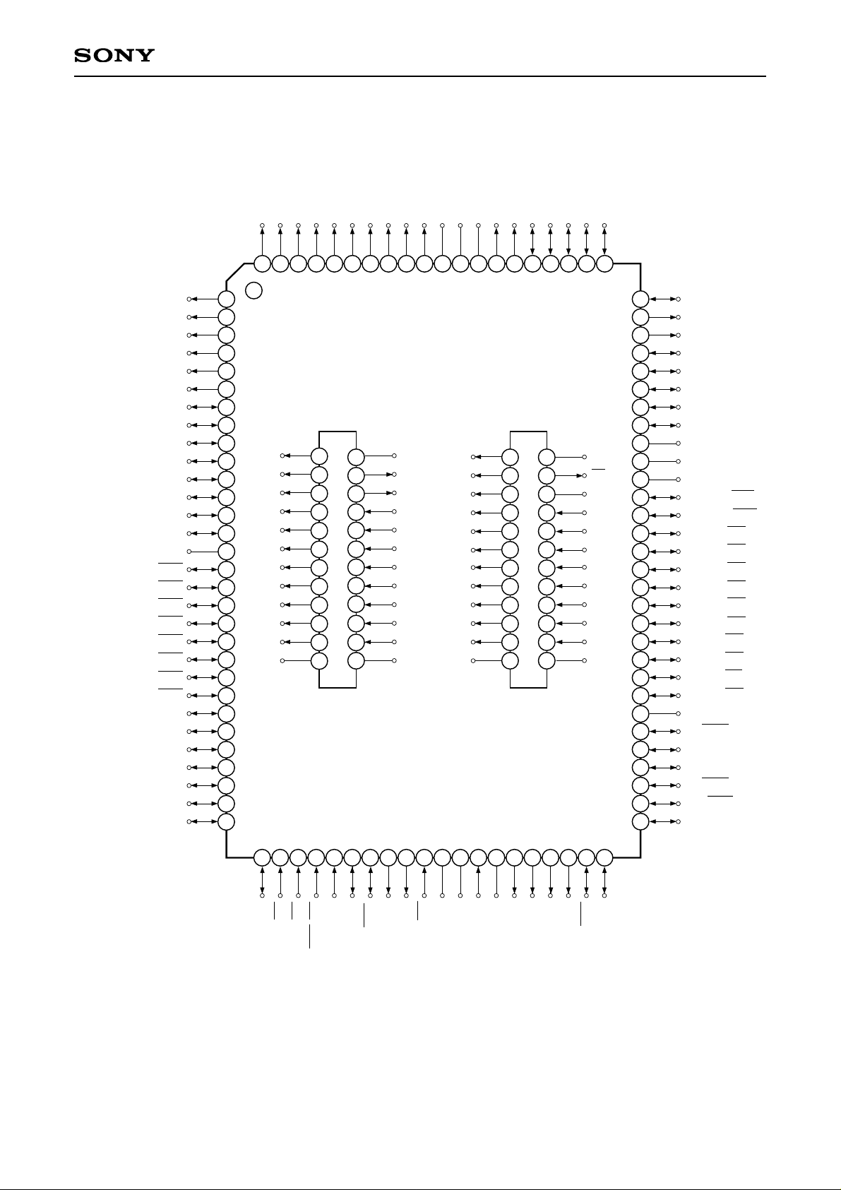
CXP971000
Pin Assignment in Piggyback Mode (Top View) 100-pin QFP package
31 32 33 34 35 36 37 38 39 404142 43 44 45
46
47
48 49 50
57
58
59
60
61
62
63
64
65
66
67
68
69
70
71
72
73
74
75
76
77
78
79
80
81828384858687888990919293949596979899
1
2
3
4
5
6
7
8
9
10
11
12
13
14
15
16
17
18
19
20
21
22
23
24
PE7/INT7/CINT
PF0/EC0
PF1/EC2
PF2/SCS1/NMI
PF3/SI1
PF4/SO1
PF5/SCK1
PF6/T1
PF7/T2
RST
V
SS
XTAL
EXTAL
V
DD
PG0/PWM0
PG1/PWM1
PG2/PWM2
PG3/PWM3
PG4/SCS0
PG5/SI0
PH0/SDA
PK6
PK5
PK4/ADTRG
PK3/ADTEN
PK2
PK1
PK0
AV
DD
AVREF
AVSS
PJ7/AN11/KS11
PJ6/AN10/KS10
PJ5/AN9/KS9
PJ4/AN8/KS8
PJ3/AN7/KS7
PJ2/AN6/KS6
PJ1/AN5/KS5
PJ0/AN4/KS4
PI7/AN3/KS3
PI6/AN2/KS2
PI5/AN1/KS1
PI4/AN0/KS0
Vss
PI3/SCK2
51
52
53
54
55
56
PI2/SO2
PI1/SI2
PI0/SCS2
PG7/SCK0
PG6/SO0
PB2/PPO02/A10
PB3/PPO03/A11
PB4/PPO04/A12
PB5/PPO05/A13
PB6/PPO06/A14
PB7/PPO07/A15
PC0/PPO08
PC1/PPO09
PC2/PPO10
PC3/PPO11
PC4/PPO12/XCS3
PC5/PPO13/XCS2
PC6/PPO14/XCS1
PC7/PPO15/XCS0
V
SS
PD0/D0/KS12
PD1/D1/KS13
PD2/D2/KS14
PD3/D3/KS15
PD4/D4/KS16
PD5/D5/KS17
PD6/D6/KS18
PD7/D7/KS19
PE0/INT0
25
26
27
28
29
PE1/INT1
PE2/INT2
PE3/INT3
PE4/INT4
PE5/INT5
30
PE6/INT6
PB1/PPO01/A9
PB0/PPO00/A8
PA7/A7
PA6/A6
PA5/A5
PA4/A4
PA3/A3
PA2/A2
PA1/A1
PA0/A0
VSSVDDNCPH7/XRD
PH6/XWR
PH5
PH4/RMC
PH3/TxD
PH2/RxD
PH1/SCL
100
1
2
3
4
5
6
7
8
9
10
11
12
13
14
15
16
17
18
19
20
21
22
23
24
A10
A9
A8
A7
A6
A5
A4
A3
A2
A1
A0
Vss
VDD
A11
A12
D7
D6
D5
D4
D3
D2
D1
D0
Vss
25
26
27
28
29
30
31
32
33
34
35
36 37
38
39
40
41
42
43
44
45
46
47
48
A23
A22
A21
A20
A19
A18
A17
A16
A15
A14
A13
Vss
VDD
CE
NC
D15
D14
D13
D12
D11
D10
D9
D8
Vss
Note) 1. NC (Pin 88) must be left open. However, use this pin for FLASH EEPROM
incorporated version.
2. Vss and AVss (Pins 15, 41, 57, 70 and 90) must be connected to GND.
3. VDD and AVDD (Pins 44, 72 and 89) must be connected to VDD.
– 3 –
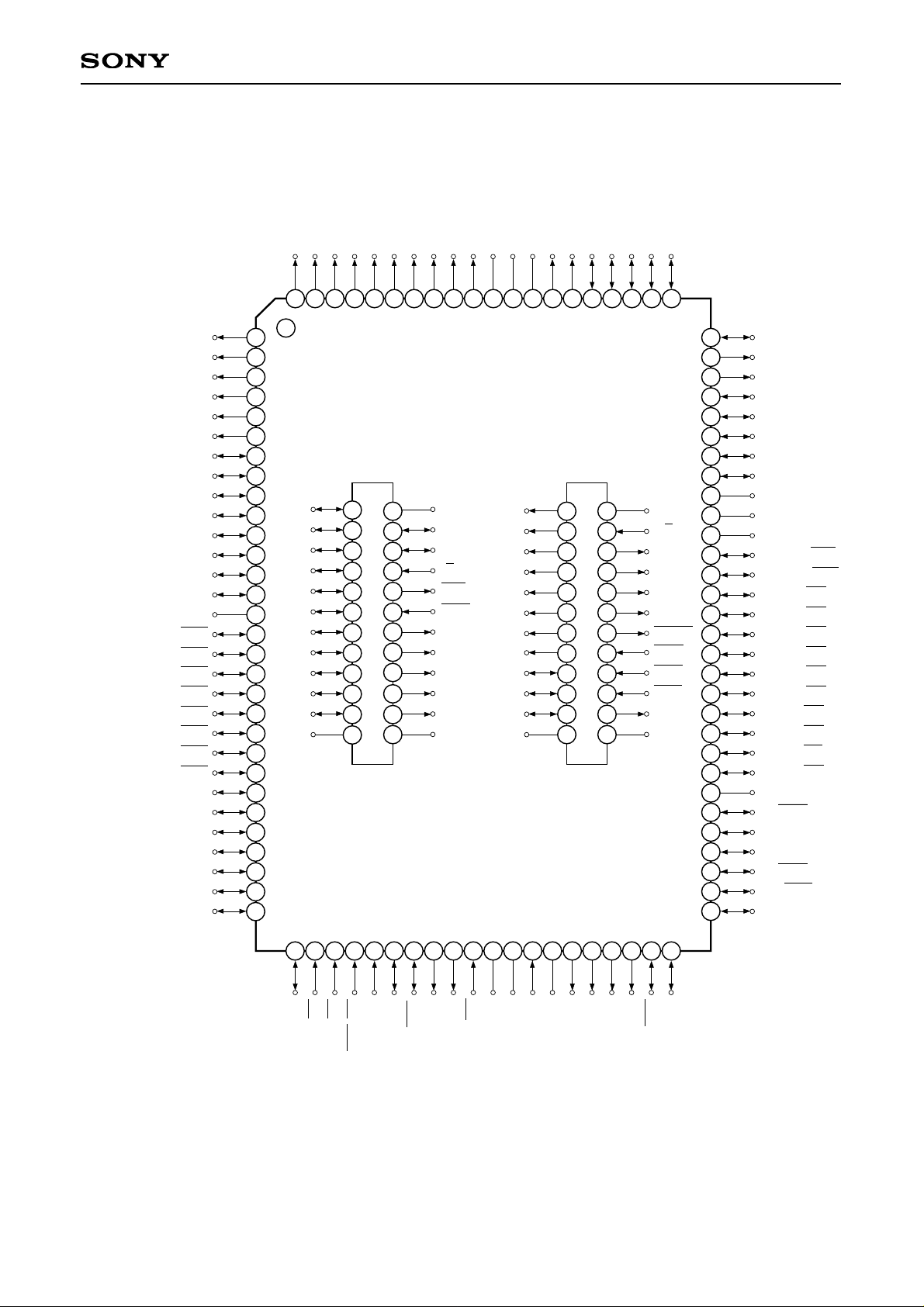
CXP971000
31 32 33 34 35 36 37 38 39 404142 43 44 45
46
47
48 49 50
57
58
59
60
61
62
63
64
65
66
67
68
69
70
71
72
73
74
75
76
77
78
79
80
81828384858687888990919293949596979899
1
2
3
4
5
6
7
8
9
10
11
12
13
14
15
16
17
18
19
20
21
22
23
24
PE7/INT7/CINT
PF0/EC0
PF1/EC2
PF2/SCS1/NMI
PF3/SI1
PF4/SO1
PF5/SCK1
PF6/T1
PF7/T2
RST
V
SS
XTAL
EXTAL
V
DD
PG0/PWM0
PG1/PWM1
PG2/PWM2
PG3/PWM3
PG4/SCS0
PG5/SI0
PH0/SDA
PK6
PK5
PK4/ADTRG
PK3/ADTEN
PK2
PK1
PK0
AV
DD
AVREF
AVSS
PJ7/AN11/KS11
PJ6/AN10/KS10
PJ5/AN9/KS9
PJ4/AN8/KS8
PJ3/AN7/KS7
PJ2/AN6/KS6
PJ1/AN5/KS5
PJ0/AN4/KS4
PI7/AN3/KS3
PI6/AN2/KS2
PI5/AN1/KS1
PI4/AN0/KS0
Vss
PI3/SCK2
51
52
53
54
55
56
PI2/SO2
PI1/SI2
PI0/SCS2
PG7/SCK0
PG6/SO0
PB2/PPO02/A10
PB3/PPO03/A11
PB4/PPO04/A12
PB5/PPO05/A13
PB6/PPO06/A14
PB7/PPO07/A15
PC0/PPO08
PC1/PPO09
PC2/PPO10
PC3/PPO11
PC4/PPO12/XCS3
PC5/PPO13/XCS2
PC6/PPO14/XCS1
PC7/PPO15/XCS0
V
SS
PD0/D0/KS12
PD1/D1/KS13
PD2/D2/KS14
PD3/D3/KS15
PD4/D4/KS16
PD5/D5/KS17
PD6/D6/KS18
PD7/D7/KS19
PE0/INT0
25
26
27
28
29
PE1/INT1
PE2/INT2
PE3/INT3
PE4/INT4
PE5/INT5
30
PE6/INT6
PB1/PPO01/A9
PB0/PPO00/A8
PA7/A7
PA6/A6
PA5/A5
PA4/A4
PA3/A3
PA2/A2
PA1/A1
PA0/A0
VSSVDDNCPH7/XRD
PH6/XWR
PH5
PH4/RMC
PH3/TxD
PH2/RxD
PH1/SCL
100
1
2
3
4
5
6
7
8
9
10
11
12
13
14
15
16
17
18
19
20
21
22
23
24
AD10
AD9
AD8
AD7
AD6
AD5
AD4
AD3
AD2
AD1
AD0
Vss
VDD
AD11
AD12
I/T
MON
ERST
C1
C2
QS0
QS1
QS2
Vss
25
26
27
28
29
30
31
32
33
34
35
36 37
38
39
40
41
42
43
44
45
46
47
48
A23
A22
A21
A20
A19
A18
A17
A16
AD15
AD14
AD13
Vss
VDD
E/P
ST0
ST1
ST2
ST3
WTACK
JRQH
JRQL
ENMI
MS
Vss
Pin Assignment in Evaluator Mode (Top View) 100-pin QFP package
Note) 1. NC (Pin 88) must be left open. However, use this pin for FLASH EEPROM
incorporated version.
2. Vss and AVss (Pins 15, 41, 57, 70 and 90) must be connected to GND.
3. VDD and AVDD (Pins 44, 72 and 89) must be connected to VDD.
– 4 –
 Loading...