

Sony CXP922032 Datasheet

– 1 –
E98Y43-PS
Sony reserves the right to change products and specifications without prior notice. This information does not convey any license by
any implication or otherwise under any patents or other right. Application circuits shown, if any, are typical examples illustrating the
operation of the devices. Sony cannot assume responsibility for any problems arising out of the use of these circuits.
CXP922032
CMOS 16-bit Single Chip Microcomputer
Description
The CXP922032 is a CMOS 16-bit microcomputer
integrating on a single chip an A/D converter, serial
interface, timer, remote control receive circuit, PWM
output circuit, and as well as basic configurations like
a 16-bit CPU, ROM, RAM, and I/O port.
This LSI also provides the sleep/stop functions that
enable lower power consumption.
Features
• An efficient instruction set as a controller
— Direct addressing, numerous abbreviated forms, multiplication and division instructions
• Instruction sets for C language and RTOS
— Highly quadratic instruction system, general-purpose register of eight 16-bit × 16-bank configuration
• Minimum instruction cycle 100ns/20MHz operation (3.0 to 5.5V)
167ns/12MHz operation (2.7 to 5.5V)
• Incorporated ROM capacity 128K bytes
• Incorporated RAM capacity 7680 bytes
• Peripheral functions
— A/D converter
8-bit 8 analog input, successive approximation system (Conversion time:
12.4µs at 20MHz)
— Serial interface Asynchronous serial interface (Simple UART)
128-byte buffer RAM,3 channels
— Timers 8-bit timer/counter, 2 channels (with timing output)
16-bit capture timer/counter (with timing output)
16-bit timer, 4 channels
— Remote control receive circuit 8-bit pulse measurement counter, 8-stage FIFO
— PWM output circuit 14-bit, 1 channel
• Interruption 24 factors, 24 vectors, multi-interruption and priority selection possible
• Standby mode Sleep/stop
• Package 100-pin plastic QFP
• Piggy/evaluation chip CXP922000
•
One-time PROM incorporated version
CXP922P032
Structure
Silicon gate CMOS IC
100 pin QFP (Plastic)
For the availability of this product, please contact the sales office.
– 2 –
CXP922032
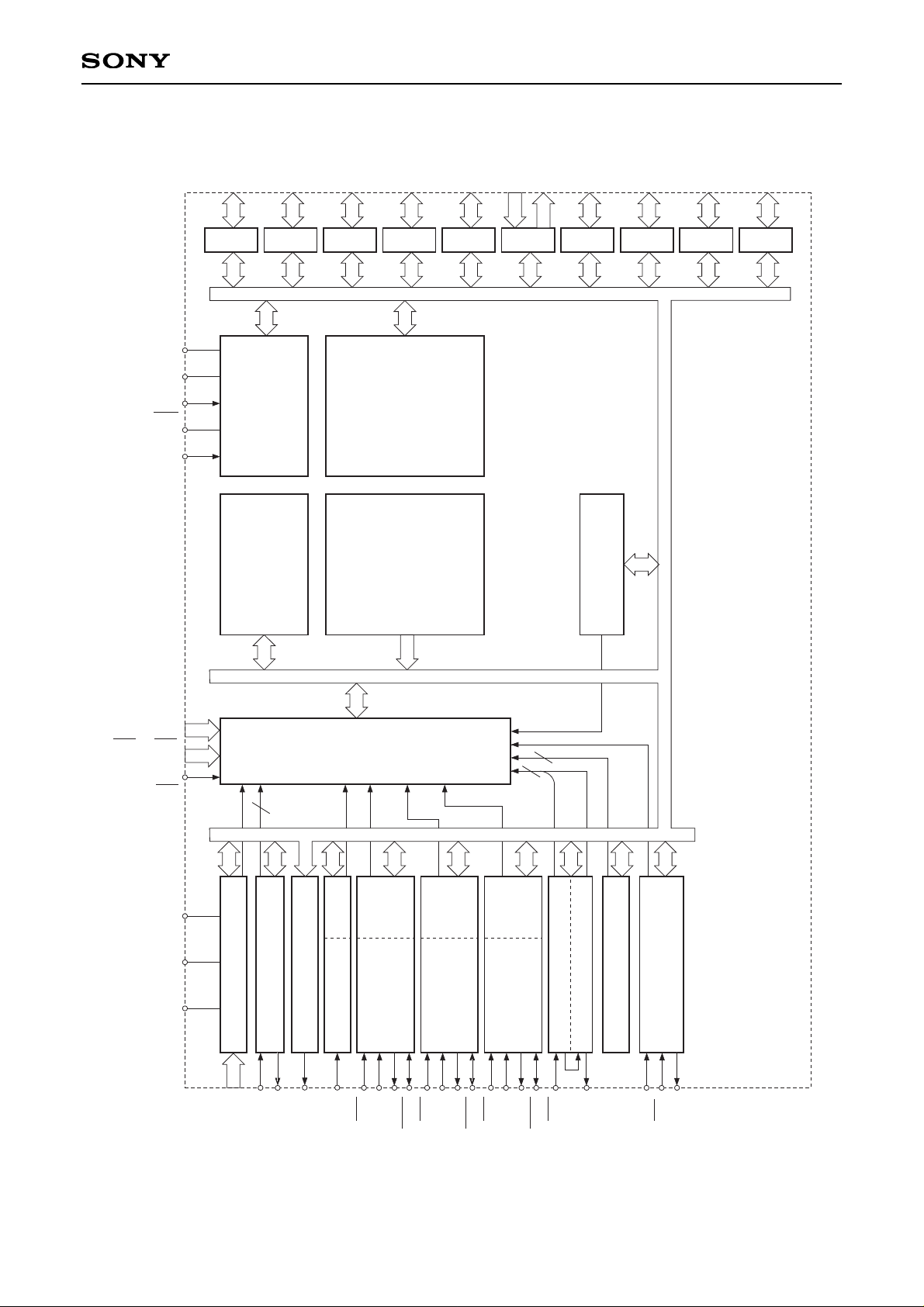
Block Diagram
A/D CONVERTER
8
5 7
AN0 to AN7 PA0 to PA7
VSS
VDD
AVREF
AVSS
AVDD
RST
XTAL
EXTAL
NMI
INT0 to INT4
PB0 to PB7
PC0 to PC7
PD0 to PD7
PE0 to PE7
PF0 to PF5
PF6, PF7
PG0 to PG7
PH0 to PH7
PI0 to PI7
PJ0 to PJ6
RxD
TxD
PWM
RMC
CS0
SO0
SI0
SCK0
SI1
CS1
SCK1
SO1
CS2
SO2
SI2
SCK2
TO0
EC0
EC1
CINT
TO1
SPC950
CPU CORE
CLOCK GENERATOR/
SYSTEM CONTROLLER
PORT A
UART
14-BIT PWM GENERATOR
REMOCON
4CH 16-BIT TIMER
FIFO
SERIAL
INTERFACE
UNIT (CH0)
BUFFER
RAM
SERIAL
INTERFACE
UNIT (CH1)
BUFFER
RAM
SERIAL
INTERFACE
UNIT (CH2)
BUFFER
RAM
8-BIT TIMER/COUNTER (CH0)
8-BIT TIMER (CH1)
16-BIT CAPTURE
TIMER/COUNTER (CH4)
PRESCALER/
TIME-BASE TIMER
2
ROM
128K BYTES
8
PORT B
8
PORT C
8
PORT D
INTERRUPT CONTROLLER
8
PORT E
8
PORT F
6
2
PORT G
8
PORT H
8
PORT I
8
PORT J
7
RAM
7680 BYTES
KS0 to KS6
2
4
– 3 –
CXP922032
Pin Assignment (Top View) 100-pin QFP package
31 32 33 34 35 36 37 38 39 40 41 42 43 44 454647 48 49 50
57
58
59
60
61
62
63
64
65
66
67
68
69
70
71
72
73
74
75
76
77
78
79
80
81828384858687888990919293949596979899
1
2
3
4
5
6
7
8
9
10
11
12
13
14
15
16
17
18
19
20
21
22
23
24
PE7
PF0/INT0
PF1/INT1
PF2/INT2
PF3/INT3
PF4/INT4
PF5/NMI
PF6/TO0
PF7/TO1/PWM
RST
V
SS
XTAL
EXTAL
V
DD
AN0
AN1
AN2
AN3
PG0/AN4
PG1/AN5
PI7/RMC
PI6/CINT
PI5/EC1
PI4/EC0
PI3
PI2
PI1/RxD
PI0/TxD
PH7/SCK2
PH6/SO2
PH5/SI2
PH4/CS2
PH3/SCK1
PH2/SO1
PH1/SI1
PH0/CS1
V
SS
SCK0
SO0
SI0
CS0
PG7
PG6
PG5
PG4
51
52
53
54
55
56
AV
DD
AVREF
AVSS
PG3/AN7
PG2/AN6
PB2
PB3
PB4
PB5
PB6
PB7
PC0
PC1
PC2
PC3
PC4
PC5
PC6
PC7
V
SS
PD0
PD1
PD2
PD3
PD4
PD5
PD6
PD7
PE0
25
26
27
28
29
PE1
PE2
PE3
PE4
PE5
30
PE6
PB1
PB0
PA7
PA6
PA5
PA4
PA3
PA2
PA1
PA0
VSSVDD
NC
PJ6/KS6
PJ5/KS5
PJ4/KS4
PJ3/KS3
PJ2/KS2
PJ1/KS1
PJ0/KS0
100
Notes) 1. Do not make any connections to NC (Pin 88).
2. VSS (Pins 15, 41, 64 and 90) must be connected to GND.
3. VDD (Pins 44 and 89) must be connected to VDD.
– 4 –

CXP922032
Pin Functions
Symbol I/O
Functions
PA0 to PA7
I/O
(Port A)
8-bit I/O port.
I/O can be specified in 1-bit units.
Pull-up resistor is present or not through program in 4-bit units.
(8 pins)
PB0 to PB7 I/O
(Port B)
8-bit I/O port.
I/O can be specified in 1-bit units.
Pull-up resistor is present or not through program in 4-bit units.
(8 pins)
PC0 to PC7 I/O
(Port C)
8-bit I/O port.
I/O can be specified in 1-bit units.
Pull-up resistor is present or not through program in 4-bit units.
(8 pins)
PD0 to PD7
I/O
(Port D)
8-bit I/O port.
I/O can be specified in 1-bit units.
Pull-up resistor is present or not through program in 4-bit units.
Can drive 12mA sink current (VDD = 4.5 to 5.5V).
(8 pins)
PE0 to PE7
I/O
(Port E)
8-bit I/O port.
I/O can be specified in 1-bit units.
Pull-up resistor is present or not through program in 4-bit units.
Can drive 12mA sink current (VDD = 4.5 to 5.5V).
(8 pins)
(Port F)
8-bit port.
Lower 6 bits are for input;
upper 2 bits are for output.
(6 pins)
PF0/INT0
to PF4/INT4
Input / Input
External interrupt inputs.
(4 pins)
PF5/NMI
Input / Input
Non-maskable interrupt input.
PF6/TO0
Output / Output
8-bit timer/counter output.
PF7/TO1/
PWM
Output / Output /
Output
16-bit capture timer/
counter output.
AN0 to AN3
Input
Analog input for A/D converter.
(4 pins)
Analog input for A/D
converter.
(4 pins)
PG0/AN4
to PG3/AN7
I/O / Input
PG4 to PG7
I/O
(Port G)
8-bit I/O port.
I/O can be specified in 1-bit units.
Pull-up resistor is present or not through
program in 4-bit units.
(8 pins)
14-bit PWM output.
CS0
SI0
SO0
SCK0
Input
Input
Output
I/O
Serial chip select (CH0) input.
Serial data (CH0) input.
Serial data (CH0) output.
Serial clock (CH0) I/O.
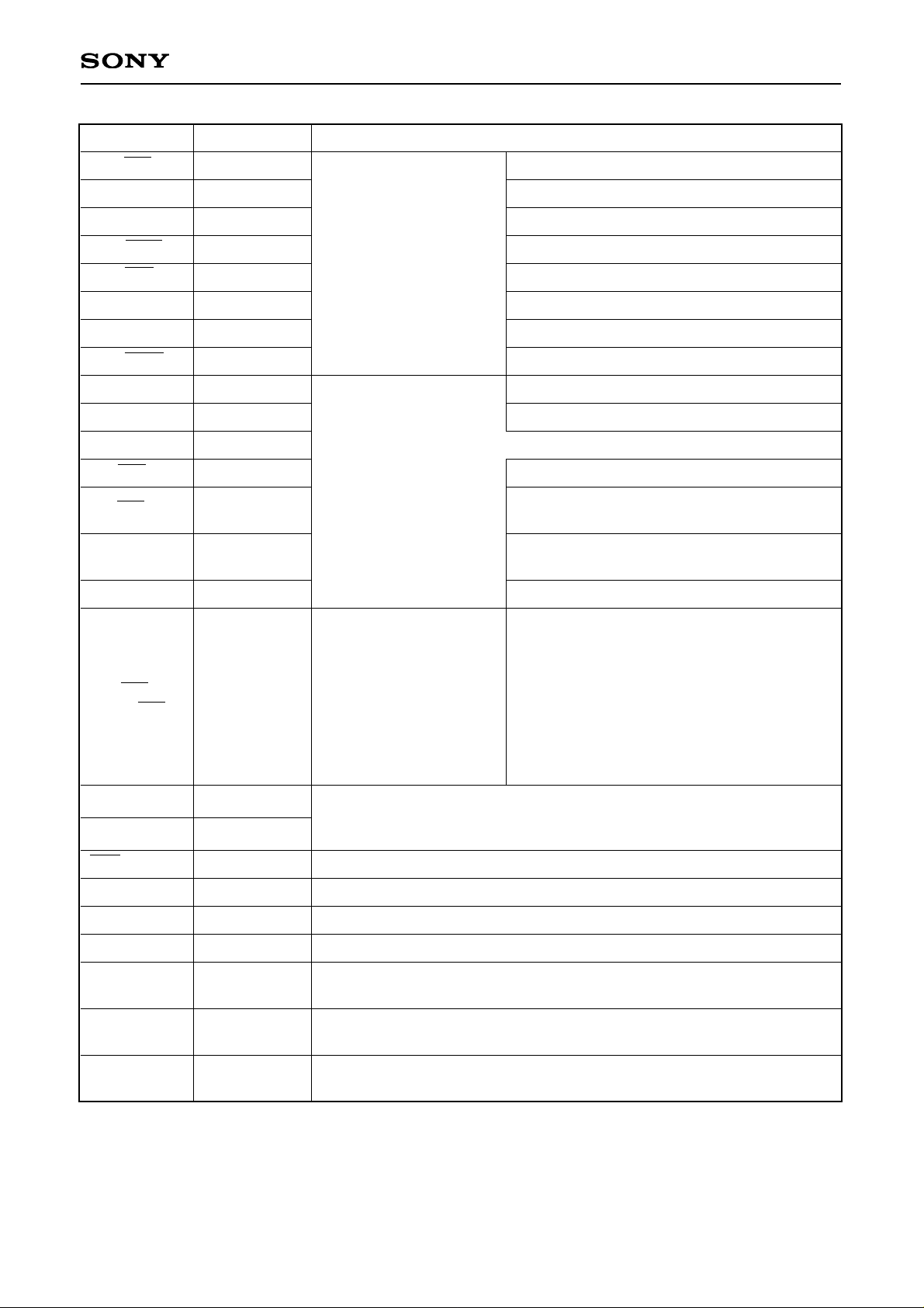
– 5 –
CXP922032
Symbol I/O
Functions
PH0/CS1
PH1/SI1
PH2/SO1
PH3/SCK1
PH4/CS2
PH5/SI2
PH6/SO2
PH7/SCK2
PI0/TxD
PI1/RxD
PI2 to PI3
PI4/EC0
PI5/EC1
PI6/CINT
PI7/RMC
PJ0/KS0
to PJ6/KS6
I/O / Input
I/O / Input
I/O / Output
I/O / I/O
I/O / Input
I/O / Input
I/O / Output
I/O / I/O
I/O / Output
I/O / Input
I/O
I/O / Input
I/O / Input
I/O / Input
I/O / Input
I/O / Input
(Port H)
8-bit I/O port.
I/O can be specified in
1-bit units.
Pull-up resistor is present
or not through
program in 4-bit units.
(8 pins)
(Port I)
8-bit I/O port.
I/O can be specified in
1-bit units.
Pull-up resistor is present
or not through
program in 4-bit units.
(8 pins)
(Port J)
7-bit I/O port.
I/O can be specified in
1-bit units.
Pull-up resistor is present
or not through
program in lower 4-bit
units and upper 3-bit units.
(7 pins)
Serial chip select (CH1) input.
Serial data (CH1) input.
Serial data (CH1) output.
Serial clock (CH1) I/O.
Serial chip select (CH2) input.
Serial data (CH2) input.
Serial data (CH2) output.
Serial clock (CH2) I/O.
UART transmission data output.
UART reception data input.
External event input for 8-bit timer/counter.
External event input for 16-bit capture timer/
counter.
External capture input for 16-bit capture timer/
counter.
Remote control receive circuit input.
Standby release input function can be specified
in 1-bit units.
(7 pins)
EXTAL
XTAL
RST
AVDD
AVREF
AVSS
VDD
VSS
NC
Input
Input
Input
Connects a crystal for system clock oscillation.
(When the clock is supplied externally, input it to EXTAL and input an
opposite phase clock to XTAL.)
System reset. Active at "L" level.
Positive power supply for A/D converter.
Reference voltage input for A/D converter.
GND for A/D converter.
Positive power supply.
(Connect both VDD pins to positive power supply.)
GND
(Connect all four VSS pins to GND.)
NC.
(Do not make any cunnection to NC.)
– 6 –
CXP922032
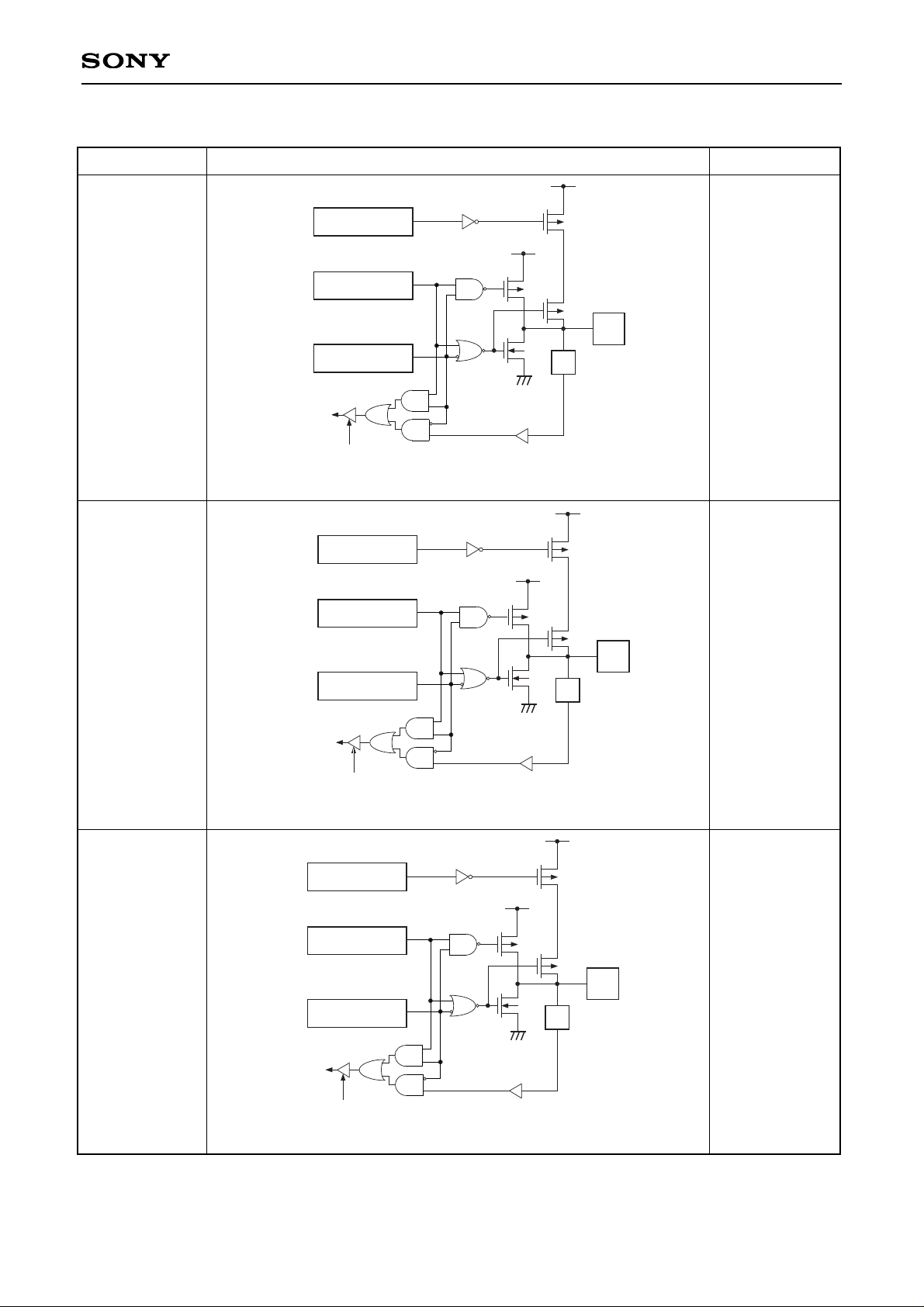
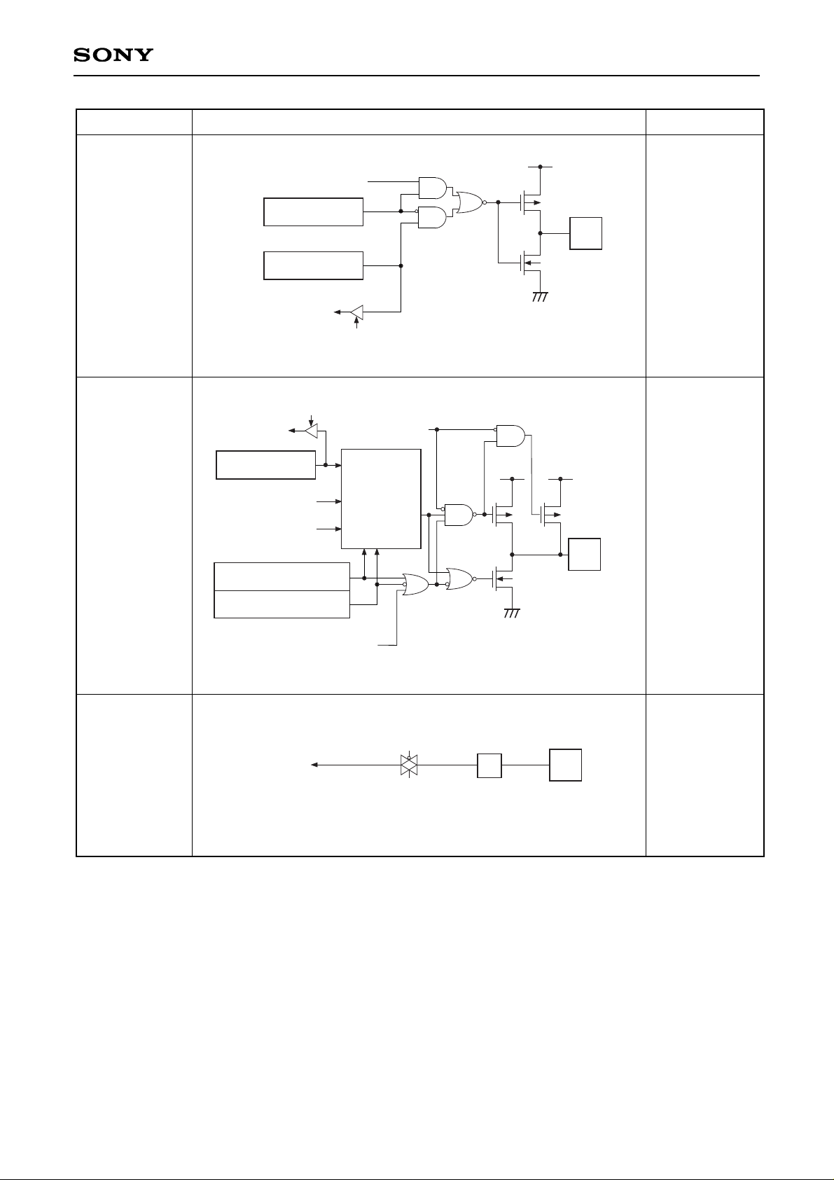
I/O Circuit Format for Pins
Pin Circuit format
After a reset
PA0 to PA7
Hi-Z
PUL0 register
"0" after a reset
Internal data bus
Input protection
circuit
IP
∗
∗
Pull-up transistor
approximately 100kΩ (V
DD = 4.5 to 5.5V)
approximately 150kΩ (V
DD = 3.0 to 3.6V)
RD
PA register
Undefined after a reset
PAD register
"0" after a reset
PB0 to PB7 Hi-Z
PUL0 register
"0" after a reset
Internal data bus
IP
∗
∗
Pull-up transistor
approximately 100kΩ (V
DD = 4.5 to 5.5V)
approximately 150kΩ (V
DD = 3.0 to 3.6V)
RD
PB register
Undefined after a reset
PBD register
"0" after a reset
PC0 to PC7 Hi-Z
PUL0 register
"0" after a reset
Internal data bus
IP
∗
∗
Pull-up transistor
approximately 100kΩ (V
DD = 4.5 to 5.5V)
approximately 150kΩ (V
DD = 3.0 to 3.6V)
RD
PC register
Undefined after a reset
PCD register
"0" after a reset

– 7 –
CXP922032
Pin
Circuit format After a reset
PD0 to PD7
Hi-Z
PF0/INT0
to PF4/INT4
PF5/NMI
Hi-Z
PUL0 register
"0" after a reset
Internal data bus
IP
∗
1
Pull-up transistor
approximately 100kΩ (V
DD = 4.5 to 5.5V)
approximately 150kΩ (V
DD = 3.0 to 3.6V)
∗
2
Large current drive
12mA (V
DD = 4.5 to 5.5V)
4.5mA (V
DD = 3.0 to 3.6V)
RD
∗1
∗2
PD register
Undefined after a reset
PDD register
"0" after a reset
PE0 to PE7
Hi-Z
PUL1 register
"0" after a reset
Internal data bus
IP
∗
1
Pull-up transistor
approximately 100kΩ (V
DD = 4.5 to 5.5V)
approximately 150kΩ (V
DD = 3.0 to 3.6V)
∗
2
Large current drive
12mA (V
DD = 4.5 to 5.5V)
4.5mA (V
DD = 3.0 to 3.6V)
RD
∗1
∗2
PE register
Undefined after a reset
PED register
"0" after a reset
Internal data bus
CMOS Schmitt input
RD
INT0, INT1, INT2,
INT3, INT4, NMI
IP
– 8 –
CXP922032
Pin
Circuit format After a reset
PF6/TO0
"H" level
PF7/TO1/
PWM
"H" level
("H" level at ON
resistance of
pull-up transistor
during a reset.)
TO0
RD
Internal data bus
PFSL register
"0" after a reset
PF register
"1" after a reset
PFSL register (Bit 7)
PFSL register (Bit 6)
TO1 output enable
TO1
PWM
∗
Pull-up transistor
approximately 150kΩ (V
DD = 4.5 to 5.5V)
approximately 200kΩ (V
DD = 3.0 to 3.6V)
RD
Internal data bus Internal reset signal
∗
01
MPX
1x
00
PF register
"1" after a reset
"00" after a reset
Hi-Z
AN0 to AN3
IP
A/D converter
Input multiplexer
– 9 –
CXP922032
Pin Circuit format
After a reset
PG0/AN4
to PG3/AN7
Hi-Z
∗
∗
Pull-up transistor
approximately 100kΩ (V
DD = 4.5 to 5.5V)
approximately 150kΩ (V
DD = 3.0 to 3.6V)
Internal data bus
IP
RD
A/D converter
Input multiplexer
PUL1 register
"0" after a reset
PG register
Undefined after a reset
PGSL register
"0" after a reset
PGD register
"0" after a reset
PG4 to PG7 Hi-Z
PUL1 register
"0" after a reset
Internal data bus
IP
∗
∗
Pull-up transistor
approximately 100kΩ (V
DD = 4.5 to 5.5V)
approximately 150kΩ (V
DD = 3.0 to 3.6V)
RD
PG register
Undefined after a reset
PGD register
"0" after a reset
 Loading...