

Sony CXP922000 Datasheet

CMOS 16-bit Single Chip Microcomputer
Description
The CXP922000 is a CMOS 16-bit single chip
microcomputer of piggyback/evaluator combined
type, which is developed for evaluating the function
of the CXP922032.
Features
• An efficient instruction set as a controller
– Direct addressing, numerous abbreviated forms,
multiplication and division instructions
• Instruction sets for C Ianguage and RTOS
– Highly quadratic instruction system,
general-purpose register of eight 16-bit × 16-bank configuration
• Minimum instruction cycle time 100ns at 20MHz operation (3.0 to 5.5V)
167ns at 12MHz operation (2.7 to 5.5V)
• Incorporated EPROM CXP27V1000K
• Incorporated RAM capacity 7680 bytes
• Peripheral functions
– A/D converter 8-bit 8 analog input, successive approximation system
(Conversion time: 12.4µs at 20MHz)
– Serial interface Asynchronous serial interface (Simple UART)
128-byte buffer RAM, 3 channels
– Timers 8-bit timer/counter, 2 channels (with timing output)
16-bit capture timer/counter (with timing output)
16-bit timer, 4 channels
– Remote control receive circuit 8-bit pulse measurement counter, 8-stage FIFO
– PWM output circuit 14-bit, 1 channel
• Interruption 24 factors, 24 vectors, multi-interruption and priority selection possible
• Standby mode Sleep/stop
• Package 100-pin ceramic PQFP
• Mask ROM CXP922032
•
One time PROM incorporated type
CXP922P032
Structure
Silicon gate CMOS IC
– 1 –
E98Z32B9X-PS
Sony reserves the right to change products and specifications without prior notice. This information does not convey any license by
any implication or otherwise under any patents or other right. Application circuits shown, if any, are typical examples illustrating the
operation of the devices. Sony cannot assume responsibility for any problems arising out of the use of these circuits.
CXP922000
100 pin PQFP (Ceramic)
Piggy/
evaluation type
( QFP supported )
For the availability of this product, please contact the sales office.
– 2 –
CXP922000
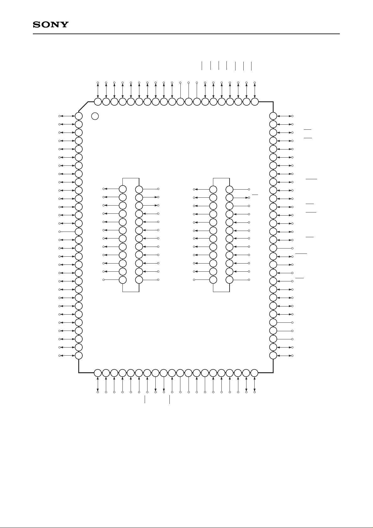
Pin Assignment in Piggyback Mode
1
2
3
4
5
6
7
8
9
10
11
12
13
14
15
16
17
18
19
20
21
22
23
24
25
26
27
28
29
30
31 32 33 34 35 36 37 38 39 40 41 42 43 44 45 46 47 48 49 50
51
52
53
54
55
56
57
58
59
60
61
62
63
64
65
66
67
68
69
70
71
72
73
74
75
76
77
78
79
80
81828384858687888990919293949596979899
100
1
2
3
4
5
6
7
8
9
10
11
12
13
14
15
16
17
18
19
20
21
22
23
24
25
26
27
28
29
30
31
32
33
34
35
36 37
38
39
40
41
42
43
44
45
46
47
48
PB1
PB0
PA7
PA6
PA5
PA4
PA3
PA2
PA1
PA0
Vss
VDD
NC
PJ6/KS6
PJ5/KS5
PJ4/KS4
PJ3/KS3
PJ2/KS2
PJ1/KS1
PJ0/KS0
PE7
PF0/INT0
PF1/INT1
PF2/INT2
PF3/INT3
PF4/INT4
PF5/NMI
PF6/TO0
PF7/TO1/PWM
RST
Vss
XTAL
EXTAL
V
DD
AN0
AN1
AN2
AN3
PG0/AN4
PG1/AN5
PB2
PB3
PB4
PB5
PB6
PB7
PC0
PC1
PC2
PC3
PC4
PC5
PC6
PC7
Vss
PD0
PD1
PD2
PD3
PD4
PD5
PD6
PD7
PE0
PE1
PE2
PE3
PE4
PE5
PE6
PI7/RMC
PI6/CINT
PI5/EC1
PI4/EC0
PI3
PI2
PI1/RxD
PI0/TxD
PH7/SCK2
PH6/SO2
PH5/SI2
PH4/CS2
PH3/SCK1
PH2/SO1
PH1/SI1
PH0/CS1
Vss
SCK0
SO0
SI0
CS0
PG7
PG6
PG5
PG4
AV
DD
AVREF
AVSS
PG3/AN7
PG2/AN6
A10
A9
A8
A7
A6
A5
A4
A3
A2
A1
A0
Vss
A23
A22
A21
A20
A19
A18
A17
A16
A15
A14
A13
Vss
VDD
A11
A12
D7
D6
D5
D4
D3
D2
D1
D0
Vss
VDD
CE
NC
D15
D14
D13
D12
D11
D10
D9
D8
Vss
Note) 1. Do not make any connections to NC (Pin 88 ).
2. Vss (Pins 15, 41, 64 and 90) are connected to GND.
3. VDD (Pins 44 and 89) are both connected to VDD.
4. A19 to A23 are always high level output.
– 3 –
 Loading...