

Sony CXP912032 Datasheet
– 1 –
CXP912032
E95Y30B86-PS
CMOS 16-bit Single Chip Microcomputer
Description
The CXP912032 is a CMOS 16-bit micro-computer
integrating on a single chip an A/D converter, serial
interface with an incorporated buffer RAM, highprecision timing pattern generation function, pulse
cycle measurement circuit, PWM generator, generalpurpose prescaler, vertical sync separation circuit,
and a measurement circuit which measures the
signals of capstan FG, drum FG/PG, reel FG and
other servo systems with high precision, as well as
basic configurations like a 16-bit CPU, ROM, RAM,
and I/O port.
This LSI also provides sleep/stop modes that enable
lower power consumption.
Features
• An efficient instruction set as a controller
— Direct addressing, numerous abbreviated forms,
multiplication and division instructions
• Instruction sets for C language and RTOS
— Highly quadratic instruction system, general-purpose
register of 16-bit × 8-pin × 16-bank configuration
• Minimum instruction cycle time 100ns at 20MHz
operation
• Incorporated ROM capacity 128K bytes
• Incorporated RAM capacity 6144 bytes
• Peripheral functions
— A/D converter 8-bit 12-channel successive approximation system, automatic
scanning function, 8-stage (soft) + 4-stage (hard) FIFO for
conversion results (Conversion time: 20µs at 20MHz)
— Serial interface Buffer RAM (128 bytes, supports high-speed transfer mode),
3 channels
— Timers 8-bit timer/counter + 8-bit timer (with timing output), 1 channel
16-bit capture timer/counter (with timing output), 1 channel
16-bit timer, 4 channels
— High-precision timing pattern generator PPG for 27 pins, 42 stages (max.)
PPG for 16 pins, 16 stages (max.)
RTG for 5 pins, 3 channels
— PWM/DA gate output PWM for 14 bits, 2 channels
(Repetitive frequency of 39.1kHz, 20MHz)
DA gate pulse for 14 bits, 2 channels
— Servo input control Capstan FG, drum FG/PG, reel FG
— VSYNC separator
— FRC capture unit 24-bit and 8-stage FIFO
— PWM output 14 bits, 2 channels
— General-purpose prescaler 10 bits, 1 channel
— Pulse cycle measurement circuit 1 channel with mask input
• General-purpose I/O 80 pins
(max.; when all multi-purpose pins are used as general-purpose I/O.)
• Interruption 28 factors, 28 vectors, multi-interruption and priority selection
possible
• Standby mode Sleep/stop
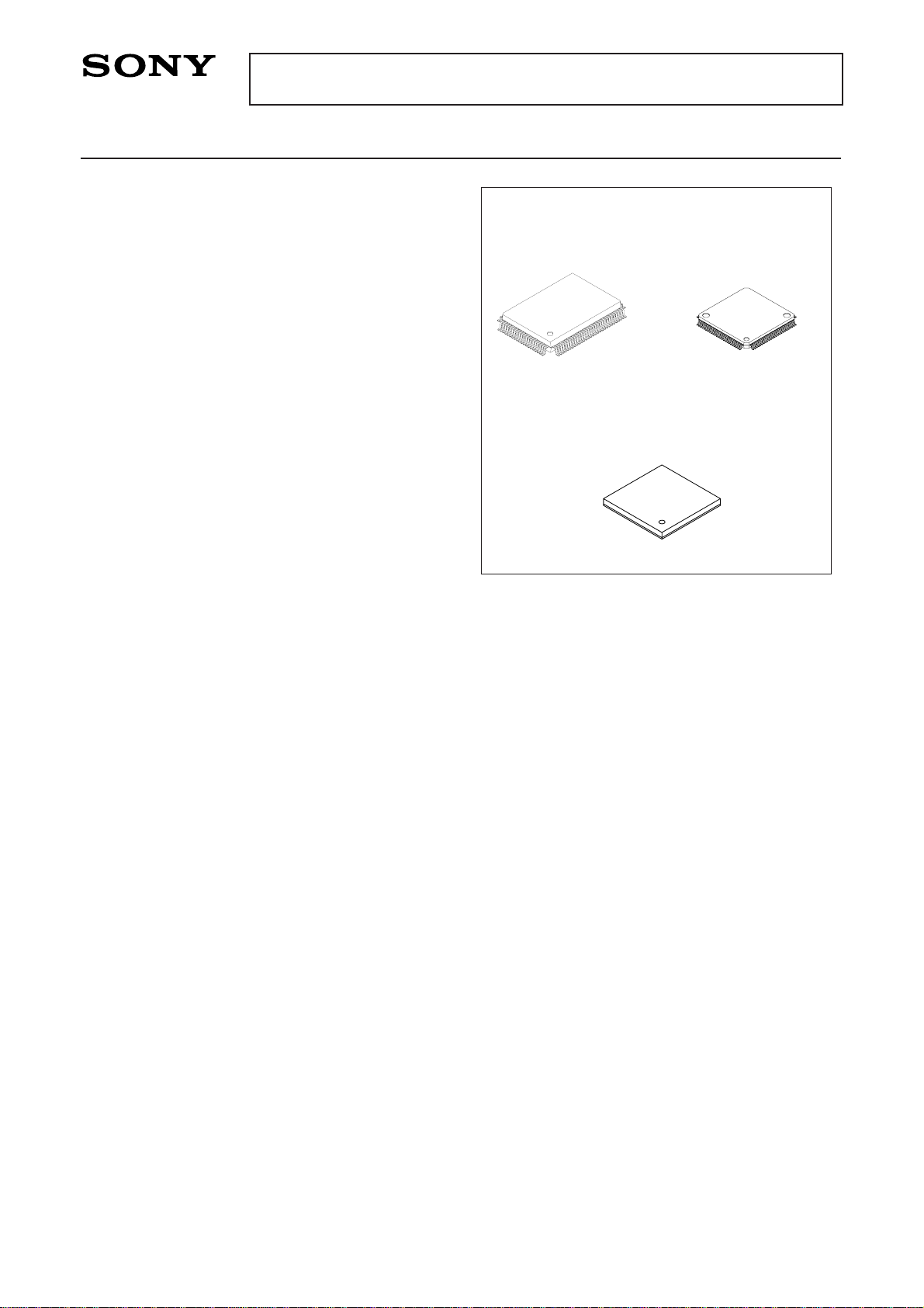
• Package 100-pin plastic QFP/LQFP, 104-pin plastic LFBGA
• Piggyback/evaluation chip CXP912000 100-pin ceramic QFP/LQFP
Sony reserves the right to change products and specifications without prior notice. This information does not convey any license by
any implication or otherwise under any patents or other right. Application circuits shown, if any, are typical examples illustrating the
operation of the devices. Sony cannot assume responsibility for any problems arising out of the use of these circuits.
100 pin QFP (Plastic)
100 pin LQFP (Plastic)
104 pin LFBGA (Plastic)
Structure
Silicon gate CMOS IC
For the availability of this product, please contact the sales office.

– 2 –
CXP912032
Vss
V
DD
CLOCK
GENERATOR/
SYSTEM
CONTROLLER
RAM
6144 BYTES
SPC900
CPU CORE
ROM
128K BYTES
FIFO
FRC
CAPTURE UNIT
5
10
4
SERIAL INTERFACE UNIT
(CH0)
RAM
8-BIT TIMER/COUNTER 0
8-BIT TIMER 1
V SYNC SEPARATOR
PULSE MEASURE UNIT
SERVO INPUT
CONTROL
CAPSTAN
DRUM
REEL
4
3
PMSK
PMI
PWM3
PWM2
DA1
PWM0
EXI1
EXI0
RFG1
RFG0
CFG
SYNC1
SYNC0
T2
CINT
T1
EC0
SCK2
SO2
SI2
SCK1
SO1
SI1
CS1
REALTIME
PULSE
GENERATOR
NMI
INT0
RST
8
PORT A
8
PORT B
8
PORT C
8
PORT D
PORT E
4
PORT F
PORT G
8
PORT H
PORT I
EXTAL
XTAL
PRESCALER
14-BIT PWM/DA GENERATOR
(× 2ch)
SERIAL INTERFACE UNIT
(CH1)
CH0
8
PORT J
RTO0
to
RTO4
PPO100
to
PPO109
16-BIT TIMER (× 4ch)
PROGRAMMABLE
PATTERN
GENERATOR
RAM(CH1)
CH1 CH2
FIFO
FIFO
A/D
CONVERTER
4
3
2
INT1
INT2
12
19
PPO000
to
PPO018
PROGRAMMABLE PRESCALER
PROGRAMMABLE
PATTERN
GENERATOR
RAM(CH0)
4
INTERRUPT CONTROLLER
2
SERIAL INTERFACE UNIT
(CH2)
16-BIT CAPTURE TIMER/COUNTER
RAM
RAM
2
AN0
to
AN11
AV
SS
AV
REF
AV
DD
14-BIT PWM GENERATOR (× 2ch)
DA0
PWM1
XOUT
(OSCO)
PCK/OSCI
PO
DPG
DFG
EC2
SCK0
SO0
SI0
CS0
8
2
4
4
2
2
CS2
4
6
Block Diagram
– 3 –
CXP912032
Pin Configuration 1 (Top View) 100-pin QFP Package
PB2/PPO010
PB3/PPO011
PB4/PPO012
PB5/PPO013
PB6/PPO014
PB7/PPO015
PC0/PPO016
PC1/PPO017
PC2/PPO018
PC3/RTO0
PC4/RTO1
PC5/RTO2
PC6/RTO3
PC7/RTO4
VSS
PD0/KS0
PD1/KS1
PD2/KS2
PD3/KS3
PD4/KS4
PD5/KS5
PD6/KS6
PD7/KS7
PE0
PE1
PE2
PE3
PE4
PE5
PE6
PJ0/AN4/KS8
AV
DD
AVREF
AVSS
AN3
AN2
AN1
PI7/AN0
VSS
PI6/XOUT
PI5/OSCO
PI4/PCK/OSCI
PI3/CS2/PO
PI2/SCK2
PI1/SO2
PI0/SI2
SCK0
SO0
SI0
CS0
PH7/CFG
PH6/DFG
PH5/DPG
PH4/PMSK
PH3/SYNC1
PH2/SYNC0/PMI
PH1/EXI1
PH0/EXI0
PG7/RFG1
PG6/RFG0
PB1/PPO009/PPO109
PB0/PPO008/PPO108
PA7/PPO007/PPO107
PA6/PPO006/PPO106
PA5/PPO005/PPO105
PA4/PPO004/PPO104
PA3/PPO003/PPO103
PA2/PPO002/PPO102
PA1/PPO001/PPO101
PA0/PPO000/PPO100
V
SS
V
DD
NC
PJ7/AN11/KS15
PJ6/AN10/KS14
PJ5/AN9/KS13
PJ4/AN8/KS12
PJ3/AN7/KS11
PJ2/AN6/KS10
PJ1/AN5/KS9
PE7
PF0/EC0/INT0
PF1/EC2/INT1
PF2/CS1/NMI/CINT
PF3/SI1/INT2
PF4/SO1
PF5/SCK1
PF6/T1
PF7/T2
RST
V
SS
XTAL
EXTAL
V
DD
PG0/PWM0
PG1/PWM1
PG2/PWM2
PG3/PWM3
PG4/DA0
PG5/DA1
40
39
38
37
36
35
34
31
32
33
41 42
43
44
45
46
47
48
49
50
51
52
53
54
55
56
57
58
59
60
70
69
68
67
63
64
65
66
61
62
71
72
73
74
75
76
77
78
79
80
2
3
4
5
6
7
8
9
10
11
12
13
14
15
16
17
18
19
20
21
22
23
24
25
26
27
28
29
30
1
81
82
83
84
88
87
86
85
89
90
100
99
98
97
96
95
94
91
92
93
Note) 1. Vss (Pins 15, 41, 72 and 90) must be connected to GND.
2. VDD (Pins 44 and 89) must be connected to VDD.
3. NC (Pin 88) is left open.
– 4 –
CXP912032
Pin Configuration 2 (Top View) 100-pin LQFP Package
PB4/PPO012
PB5/PPO013
PB6/PPO014
PB7/PPO015
PC0/PPO016
PC1/PPO017
PC2/PPO018
PC3/RTO0
PC4/RTO1
PC5/RTO2
PC6/RTO3
PC7/RTO4
VSS
PD0/KS0
PD1/KS1
PD2/KS2
PD3/KS3
PD4/KS4
PD5/KS5
PD6/KS6
PD7/KS7
PE0
PE1
PE2
PE3
AV
SS
AN3
AN2
AN1
PI7/AN0
VSS
PI6/XOUT
PI5/OSCO
PI4/PCK/OSCI
PI3/CS2/PO
PI2/SCK2
PI1/SO2
PI0/SI2
SCK0
SO0
SI0
CS0
PH7/CFG
PH6/DFG
PH5/DPG
PH4/PMSK
PH3/SYNC1
PH2/SYNC0/PMI
PH1/EXI1
PH0/EXI0
PB3/PPO011
PB2/PPO010
PB1/PPO009/PPO109
PB0/PPO008/PPO108
PA7/PPO007/PPO107
PA6/PPO006/PPO106
PA5/PPO005/PPO105
PA4/PPO004/PPO104
PA3/PPO003/PPO103
PA2/PPO002/PPO102
PA1/PPO001/PPO101
PA0/PPO000/PPO100
V
SS
V
DD
NC
PJ7/AN11/KS15
PJ6/AN10/KS14
PJ5/AN9/KS13
PJ4/AN8/KS12
PJ3/AN7/KS11
PJ2/AN6/KS10
PJ1/AN5/KS9
PJ0/AN4/KS8
AV
DD
AV
REF
PE4
PE5
PE6
PE7
PF0/EC0/INT0
PF1/EC2/INT1
PF2/CS1/NMI/CINT
PF3/SI1/INT2
PF4/SO1
PF5/SCK1
PF6/T1
PF7/T2
RST
V
SS
XTAL
EXTAL
V
DD
PG0/PWM0
PG1/PWM1
PG2/PWM2
PG3/PWM3
PG4/DA0
PG5/DA1
PG6/RFG0
PG7/RFG1
2
3
4
5
6
7
8
9
10
11
12
13
14
15
16
17
18
19
20
21
22
23
24
25
1
76
77
78
79
80
26
27
28
29
30
40
39
38
37
36
35
34
31
32
33
41
42
43
44
45
46
47
48
49
50
81
82
83
84
88
87
86
85
89
90
100
99
98
97
96
95
94
91
92
93
51
52
53
54
55
56
57
58
59
60
70
69
68
67
63
64
65
66
61
62
71
72
73
74
75
Note) 1. Vss (Pins 13, 39, 70 and 88) must be connected to GND.
2. VDD (Pins 42 and 87) must be connected to VDD.
3. NC (Pin 86) is left open.
– 5 –
CXP912032
Pin Configuration 3 (Top View) 104-pin LFBGA Package
A11
A3
A13
A4
A5
A6
A7
A8
A9
A10
A1
B11
B3
B4
B5
B6
B7
B8
B9
B10
C2
C12
C13
C4
C5
C6
C7
C8
C9
C10
C1
D11
D2
D12
D3
D13
D1
E11
E2
E12
E3
E13
E1
F11
F2
F12
F3
F13
F1
G11
G2
G12
G3
G13
G1
H11
H2
H12
H3
H13
H1
J11
J2
J12
J3
J13
J1
K11
K2
K12
K3
K13
K1
L2
L12
L13
L4
L5
L6
L7
L8
L9
L10
L1
M11
M3
M4
M5
M6
M7
M8
M9
M10
N11
N3
N13
N4
N5
N6
N7
N8
N9
N10
N1
NC
1 2 3 4 5 6 7 8 9 10 11 12 13
A
B
C
D
E
F
G
H
J
K
L
M
N
PB1 PA7 PA4 PA1 V
SS NC PJ5 PJ2 PJ0 NC
PB2 PB0 PA5 PA2 V
DD PJ7 PJ4 PJ1 AVDD
PB6 PB5 PB3 PA6 PA3 PA0 PJ6 PJ3 AVREF AN2
PC0 PB4 AV
SS PI7
PC3 PC1 V
SS PI5
PC6 PC4 PI4 PI2
V
SS PD0 PI1 PI0
PD1 PD3
CS0
SO0
PD4 PD6 PH5 PH7
PD7 PE3 PH0 PH4
PE1 PE4 PF1 PF4 V
SS VDD PG2 PG7 PH2
PE5 PE7 PF2 PF5 PF7 EXTAL PG1 PG4 PG6
NC PE6 PF0 PF3 PF6
RST
XTAL PG0 PG3 PG5 NC
PE2
PE0
PD5
PD2
PC7
PC5
PC2
PB7
AN3
PH1
PH3
PH6
SI0
SCK0
PI3
PI6
AN1
Note) 1. Vss (Pins A7, E11, G1 and L7) must be connected to GND.
2. VDD (Pins B7 and L8) must be connected to VDD.
3. NC (Pins A1, A13, N1, N13 and A8) are left open.
4. A1, A13, N1 and N13 pins are reinforced balls.
– 6 –
CXP912032
Output /
Real time output /
Real time output
Output /
Real time output /
Real time output
Output /
Real time output
Output /
Real time output
Output /
Real time output
I/O
I/O
(Port A)
8-bit output port. Data is
gated with PPO0 and PPO1
contents by OR-gate and
they are output. (8 pins)
(Port B)
8-bit output port. Data is
gated with PPO0 and
PPO1 contents by ORgate and they are output.
(8 pins)
(Port C)
8-bit I/O port. I/O can be
specified by bit unit.
Data is gated with PPO0
or RTO contents by ORgate and they are output.
(8 pins)
(Port D)
8-bit I/O port. I/O can be specified by bit unit.
Standby release input function can also be specified by bit unit.
Can drive 12mA sync current when VDD = 5V.
(8 pins)
(Port E)
8-bit I/O port. I/O can be specified by bit unit.
Can drive 12mA sync current when VDD = 5V.
(8 pins)
(Port F)
8-bit port.
Lower 4 bits
are for input;
upper 4 bits
are for output.
(8 pins)
Programmable pattern generator (PPG0,
PPG1) output. Functions as high-precision
real-time pulse output port.
(PPG0 19 pins, PPG1 10 pins)
Real-time pulse generator (RTG) output.
Functions as high-precision real-time
pulse output port.
(5 pins)
Symbol I/O Functions
PA0/PPO000
/PPO100
to
PA7/PPO007
/PPO107
PB0/PPO008
/PPO108
PB1/PPO009
/PPO109
PB2/PPO010
to
PB7/PPO015
PC0/PPO016
to
PC2/PPO018
PC3/RTO0
to
PC7/RTO4
PD0 to PD7
PE0 to PE7
PF0/EC0/
INT0
Input / Input /
Input
Input / Input /
Input
Input / Input /
Input / Input
Input / Input /
Input
PF1/EC2/
INT1
PF2/CS1/
NMI/CINT
PF3/SI1/INT2
PF4/SO1
PF5/SCK1
PF6/T1
PF7/T2
Output / Output
Output / I/O
Output / Output
Output / Output
Pin Description
External event input for
timer/counter.
(2 pins)
Serial data (CH1) input.
Serial data (CH1) output.
Serial data (CH1) I/O.
8-bit timer/counter output.
16-bit capture timer/counter output.
Input to request external
interruption. Active at the
falling edge.
Serial chip
select (CH1)
input.
Input to request external
interruption. Active at the
falling edge.
(2 pins)
Input to request
non-maskable
interruption. Active
at the falling edge.
External capture
input for 16-bit
timer/counter.
– 7 –
CXP912032
PG0/PWM0
PG1/PWM1
PG2/PWM2
PG3/PWM3
PG4/DA0
PG5/DA1
PG6/RFG0
PG7/RFG1
PH0/EXI0
PH1/EXI1
PH2/
SYNC0/PMI
PH3/SYNC1
PH4/PMSK
PH5/DPG
PH6/DFG
PH7/CFG
SCK0
SO0
SI0
CS0
PI0/SI2
PI1/SO2
PI2/SCK2
PI3/CS2/PO
PI4/PCK/
OSCI
PI5/OSCO
PI6/XOUT
PI7/AN0
AN1 to AN3
PJ0/AN4
to
PJ7/AN11
Output / Output
Output / Output
Output / Output
Output / Output
Output / Output
Output / Output
Input / Input
Input / Input
Input / Input
Input / Input
Input / Input /
Input
Input / Input
Input / Input
Input / Input
Input / Input
Input / Input
I/O
Output
Input
Input
I/O / Input
I/O / Output
I/O / I/O
I/O / Input / Output
Input / Input /
Input
Input / Output
Input / Output
Input / Input
Input
I/O / Input
14-bit PWM output.
(4 pins)
DA gate pulse output.
(2 pins)
Reel FG input.
(2 pins)
External input for FRC capture unit.
(2 pins)
Composite sync signal
input.
(2 pins)
Mask input for pulse cycle measurement circuit.
Drum PG input.
Drum FG input.
Capstan FG input.
Serial data (CH2) input.
Serial data (CH2) output.
Serial clock (CH2) I/O.
General-purpose
prescaler external clock input.
Clock output from clock generator or general-purpose
prescaler.
Serial clock (CH0) I/O.
Serial data (CH0) output.
Serial data (CH0) input.
Serial chip select (CH0) input.
Pulse input for pulse cycle
measurement circuit.
(Port G)
8-bit port.
Lower 6 bits
are for output;
upper 2 bits
are for input.
(8 pins)
(Port H)
8-bit input
port.
(8 pins)
(Port I)
8-bit port.
Lower 4 bits
are for I/O;
upper 4 bits
are for input.
Lower 4 bits
can be
specified by
bit unit.
(8 pins)
(Port J)
8-bit I/O port. I/O can be
specified by bit unit.
Standby release input
function can also be
specified by bit unit.
(8 pins)
Analog input for A/D converter.
(12 pins)
Serial chip select
(CH2) input.
General-purpose
prescaler output.
Symbol I/O Functions
Connects a crystal for generalpurpose prescaler clock
oscillation. (Mask option)
– 8 –
CXP912032
EXTAL
XTAL
RST
AVDD
AVREF
AVSS
VDD
VSS
Input
Output
I/O
Input
Connects a crystal for system clock oscillation. When the clock is
supplied externally, input it to EXTAL and input an opposite phase
clock to XTAL.
System reset. Active at "L" level.
Positive power supply for A/D converter.
Reference voltage input for A/D converter.
A/D converter GND.
Positive power supply. All three VDD pins must be connected to the
positive power supply.
GND. All four VSS pins must be connected to GND.
Symbol I/O Functions
– 9 –
CXP912032
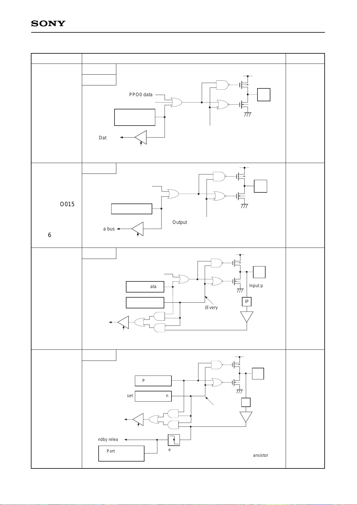
10 pins
Hi-Z
Hi-Z
After a reset
PA0/PPO000/
PPO100
to
PA7/PPO007/
PPO107
PB0/PPO008/
PPO108
to
PB1/PPO009/
PPO109
PC0/PPO016
to
PC2/PPO018
PC3/RTO0
to
PC7/RTO4
Hi-Z
PD0/KS0
to
PD7/KS7
PPO0 data
Data bus
Output becomes active from Hi-Z by
writing data to port register.
Port A or
Port B data
RD
PPO1 data
PPO0 data
Data bus
Output becomes active from Hi-Z by
writing data to port register.
Port B data
RD
PPO0 or RTO data
Data bus
RD (Port C)
Port C direction
Port C data
Input protection
circuit
IP
(Every bit)
A
"0" after a reset
Data bus
RD
Port D direction
Port D data
IP
(Every bit)
∗
Standby release
"0" after a reset
Port D standby
release data
Edge detection
∗
Large current drive transistor
6 pins
Hi-Z
PB2/PPO010
to
PB7/PPO015
I/O Circuit Format for Pins
Port A
Port B
Pin
Circuit format
8 pins
8 pins
Port B
Port C
Port D
 Loading...