

Sony CXP88748, CXP88740, CXP88732 Datasheet

Description
The CXP88732/88740/88748 is a CMOS 8-bit
microcomputer which consists of A/D converter,
serial interface, timer/counter, time base timer, high
precision timing pattern generation circuits, PWM
output, VISS/ VASS circuit, 32kHz timer/counter,
remote control receiving circuit, VSYNC separator
and the measurement circuit which measure signals
of capstan FG amplifier and drum FG/PG amplifier
and other servo systems, as well as basic
configurations like 8-bit CPU, ROM, RAM and I/O
port. They are integrated into a single chip.
Also, CXP88732/88740/88748 provides sleep/stop
function which enables to lower power consumption.
Features
• A wide instruction set (213 instructions) which cover various types of data
— 16-bit arithmetic/multiplication and division/boolean bit operation instructions
• Minimum instruction cycle 250ns at 16MHz operation
122µs at 32kHz operation
• Incorporated ROM capacity 32K bytes (CXP88732)
40K bytes (CXP88740)
48K bytes (CXP88748)
• Incorporated RAM capacity 1344 bytes (including PPG RAM)
• Peripheral function
— A/D converter 8 bits, 14 channels, successive approximation system
(Conversion time of 20µs/16MHz)
— Serial interface Incorporated 8-bit, 8-stage FIFO for data
(Auto transfer for 1 to 8 bytes), 1 channel
8-bit clock sync type, 1 channel
— Timer 8-bit timer/counter, 2 channels
19-bit time base timer
32kHz timer/counter
— High precision timing pattern generation PPG 19 pins 32-stage programmable circuit
RTG 5 pins, 1 channel
5-bit, 8-satge FIFO (RECCTL control), 1channel
— PWM/DA gate output 12 bits, 2 channels (Repetitive frequency 62.5kHz/16MHz)
DA gate pulse output, 13 bits, 2 channels
— Analog signal input circuit Capstan FG amplifier circuit
Drum FG amplifier circuit
Drum PG amplifier circuit
PBCTL amplifier circuit
— CTL write/rewrite circuit Recording current control circuit
— Servo input control Capstan FG, Drum FG/PG, CTL input
— VSYNC separator
— FRC capture unit Incorporated 26-bit and 8-stage FIFO
— PWM output 14-bit, 1 channel
— VISS/VASS circuit Pulse duty auto detection circuit
— 32kHz timer/event counter 32kHz oscillation circuit, ultra-low speed instruction mode
— Remote control reception circuit 8-bit pulse measurement counter, 6-stage FIFO
— Tri-state output PPG 1 pin, output 8 pins
— Pseudo HSYNC output function
— High speed head switching circuit
• Interruption 20 factors, 15 vectors, multi-interruption possible
• Standby mode SLEEP/STOP
• Package 100-pin plastic QFP
• Piggyback/evaluation chip CXP88800 100-pin ceramic QFP
– 1 –
CXP88732/88740/88748
100 pin QFP (Plastic)
E96109-ST
CMOS 8-bit Single Chip Microcomputer
Sony reserves the right to change products and specifications without prior notice. This information does not convey any license by
any implication or otherwise under any patents or other right. Application circuits shown, if any, are typical examples illustrating the
operation of the devices. Sony cannot assume responsibility for any problems arising out of the use of these circuits.
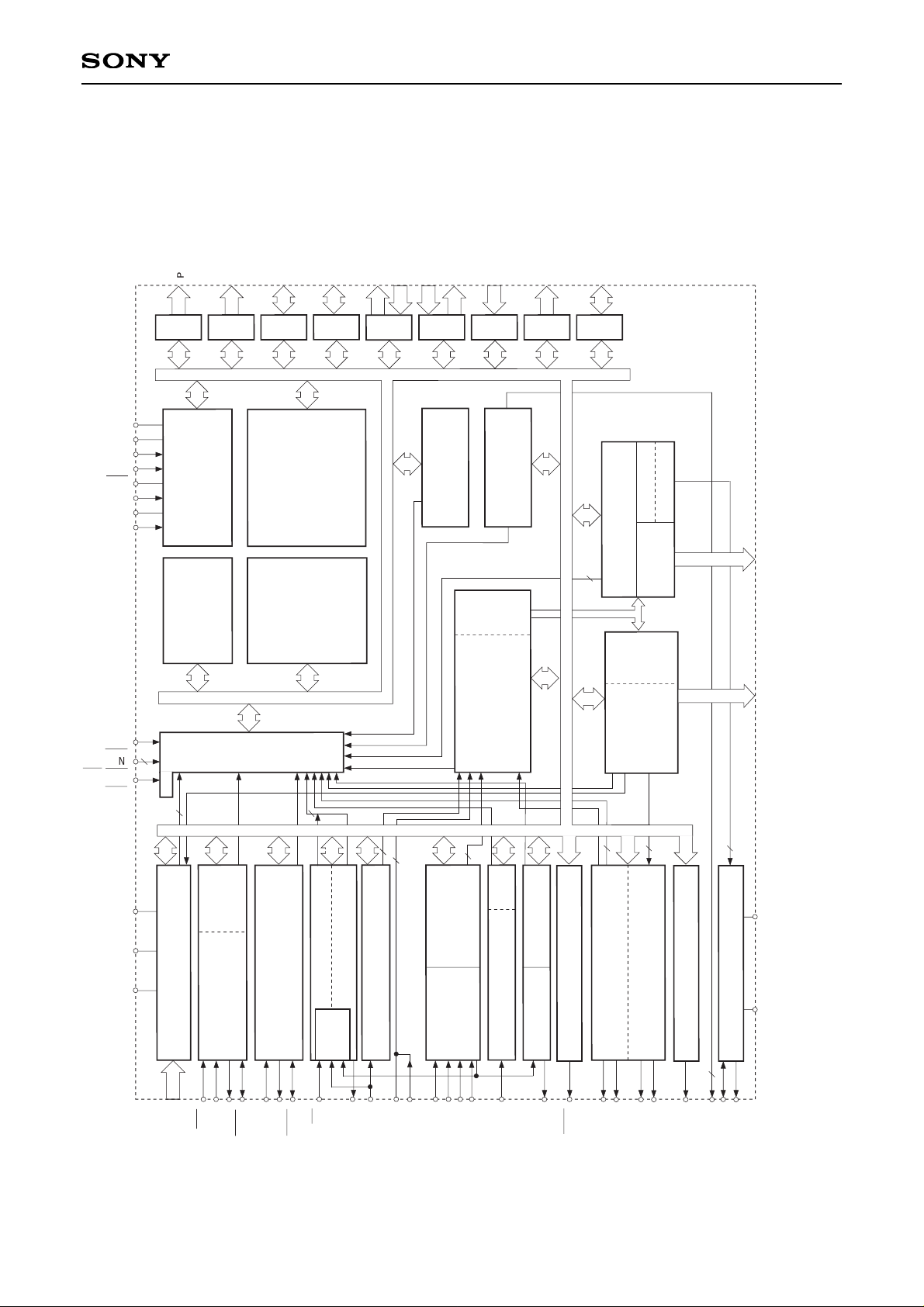
Structure
Silicon gate CMOS IC
– 2 –
CXP88732/88740/88748
SO1
PA0 to PA7
PB0 to PB7
PC0 to PC7
PD0 to PD7
PE0, 1, 6, 7
PE2 to PE5
PF0 to PF3
PF4 to PF7
PG0, 1
PI0 to PI7
Vss
V
DD
MP
RST
XTAL
EXTAL
CLOCK
GENERATOR/
SYSTEM CONTROL
RAM
1344 BYTES
SPC700
CPU CORE
ROM
32K/40K/48K BYTES
INTERRUPT CONTROLLER
2
2
FIFO
FRC
CAPTURE UNIT
PROGRAMABLE
PATTERN
GENERATOR
RAM
2
AVss
AV
REF
AV
DD
2
A/D CONVERTER
SERIAL
INTERFACE UNIT
(CH0)
FIFO
8 BIT TIMER/COUNTER 0
V SYNC SEPARATOR
14 BIT PWM GENERATOR
12 BIT PWM GENERATOR CH0
SERVO INPUT
CONTROL
GAIN
CONTROL
AMP
2
3
2
12 BIT PWM GENERATOR CH1
4
PWM1
PWM0
PWM
RMC
CTLAMP
DPG
DFG
CFG
EXI1
EXI0
SYNC
EC
SCK1
SI1
SCK0
SO0
SI0
CS0
AN0 to AN13
REALTIME PULSE
GENERATOR
INT2
INT0
14
8
PORT A
8
PORT B
8
PORT C
PORT D
4
4
PORT E
4
4
PORT F
2
PORT G
8
PORT H
8
PORT I
PH0 to PH7
TX
TEX
INT1/NMI
PRESCALER/
TIME BASE TIMER
VISS/VASS
REMOCON INPUT
FIFO
SERIAL INTERFACE UNIT
(CH1)
CH0
CH1
PPO0 to PPO18
RTO3 to RTO7
8 BIT TIMER/COUNTER1
EC
SELECT
PSEUDO HSYNC GENERATOR
HGO
32kHz
TIMER/COUNTER
2
DAA1
DAA0
TO
PULSE WIDTH
COUNTER
FIFO
8
19
5
CTL R/W CONTROL
RECCTL
CTLCIN
2
ADJ
AMPV
SS
AMPV
DD
DDO
5
NMI
Block Diagram
– 3 –
CXP88732/88740/88748
Pin Assignment (Top View)
PE5/EXI1
PH7
40
39
38
37
36
35
34
31
32
33
41
42
43
44
45
46
47
48
49
50
51
52
53
54
55
56
57
58
59
60
70
69
68
67
63
64
65
66
61
62
71
72
73
74
75
76
77
78
79
80
2
3
4
5
6
7
8
9
10
11
12
13
14
15
16
17
18
19
20
21
22
23
24
25
26
27
28
29
30
1
81
82
83
84
88
87
86
85
89
90
100
99
98
97
96
95
94
91
92
93
PE6/PWM0/DAA0
PE7/PWM1/DAA1
CFG
DFG
DPG
VREFOUT
AMPV
SS
CTLSAMPI
CTLFAMPO
CTLAG
CTLAMP (+)
CTLAMP (–)
CTLCIN (–)
CTLCIN (+)
RECCTL (+)
RECCTL (–)
AMPV
DD
RECCAP
VDD
AN0/ANOUT
AN1
AN2
AN3
PF0/AN4
PF1/AN5
AV
DD
AVREF
AVSS
PF2/AN6
PH6
PH5
PH4
PH3
PH2
PH1
PH0
MP
RST
V
SS
XTAL
EXTAL
PG1/AN13
PG0/AN12
PF7/AN11
PF6/AN10
PF5/AN9
PF4/AN8
PF3/AN7
PB5/PPO13
PB4/PPO12
PB3/PPO11
PB2/PPO10
PB1/PPO9
PB0/PPO8
PC7/RTO7
PC6/RTO6
PC5/RTO5
PC4/RTO4
PC3/RTO3
PC2/PPO18
PC1/PPO17
PC0/PPO16
PI7
PI6
PI5
PI4
PI3
PI2
PI1/EC/INT2
PI0/INT0/ENV-DET
PD7/SI0
PD6/SO0
PD5/SCK0
PD4/CS0
PD3/TO/DDO/ADJ/SRVO
PD2/PWM
PD1/RMC
PD0/INT1/NMI
PB6/PPO14
PB7/PPO15
PA0/PPO0/HGO
PA1/PPO1
PA2/PPO2
PA3/PPO3
PA4/PPO4
PA5/PPO5
PA6/PPO6
PA7/PPO7
NC
V
DD
V
SS
TX
TEX
PE0/SCK1
PE1/SO1
PE2/SI1
PE3/SYNC
PE4/EXI0
Note) 1. NC (Pin 90) is always connected to VDD.
2. VDD (Pins 61 and 89) are both connected to VDD
3. Vss (Pins 41 and 88) are both connected to GND.
4. MP (Pin 39) must be connected to GND.
– 4 –
CXP88732/88740/88748
Pin Description
(Port A)
8-bit output port. Data is
gated with PPO contents
by OR-gate and they are
output.
(8 pins)
(Port B)
8-bit output port. Data is
gated with PPO contents
by OR-gate and they are
output.
Tri-state control is possible.
(8 pins)
(Port C)
8-bit I/O port. I/O can be
set in a unit of single bits.
Data is gated with PPO or
RT contents by OR-gate
and they are output.
(8 pins)
(Port D)
8-bit I/O port. I/O can be
set in a unit of single bits.
(8 pins)
(Port E)
8-bit port. Bits 2, 3, 4 and 5
are for inputs; bits 0, 1, 6
and 7 are for outputs.
(8 pins)
Programmable pattern generator (PPG)
output. Functions as high precision realtime pulse output port.
(19 pins)
PA0 can be tri-state controlled with PPG.
Pseudo HSYNC output pin.
Real-time pulse generator (RTG) output.
Functions as high precision real-time
pulse output port.
(5 pins)
Input pin to request external interruption
and non-maskable interruption.
Remote control receiving circuit input pin.
14-bit PWM output pin.
Timer/counter, CTL duty detector, 32kHz
oscillation adjustment and servo amplifier
output pin.
Serial chip select (CH0) input pin.
Serial clock (CH0) I/O pin.
Serial data (CH0) output pin.
Serial data (CH0) input pin.
Serial clock (CH1) I/O pin
Serial data (CH1) output pin
Serial data (CH1) input pin
Composite sync signal input pin.
External input pin for FRC capture unit.
(2 pins)
Symbol I/O Description
PA0/PPO0
/HGO
PA1/PPO1
to
PA7/PPO7
PB0/PPO8
to
PB7/PPO15
PC0/PPO16
to
PC2/PPO18
PC3/RTO3
to
PC7/RTO7
PD0/INT1/
NMI
PD1/RMC
PD2/PWM
PD3 /TO
DDO/ADJ
SRVO
PD4/CS0
PD5/SCK0
PD6/SO0
PD7/SI0
PE0/SCK1
PE1/SO1
PE2/SI1
PE3/SYNC
PE4/EXI0
PE5/EXI1
PE6/PWM0/
DAA0
PE7/PWM1/
DAA1
PWM output pin.
(2 pins)
DA gate pulse
output pin.
(2 pins)
Output/Real-time
output/Output
Output/
Real-time output
Output/
Real-time output
I/O/
Real-time output
I/O/
Real-time output
I/O/Input/Input
I/O/Input
I/O/Output
I/O/Output/Output/
Output/Output
I/O/Input
I/O/I/O
I/O/Output
I/O/Input
Output/I/O
Output/Output
Input/Input
Input/Input
Input/Input
Input/Input
Output/Output
Output/Output
– 5 –
CXP88732/88740/88748
AN0/ANOUT
AN1 to AN3
PF0/AN4
to
PF3/AN7
PF4/AN8
to
PF7/AN11
PG0/AN12
PG1/AN13
PH0 to PH7
PI0/INT0/
ENV-DET
PI1/EC/
INT2
PI2 to PI7
CFG
DFG
DPG
RECCTL (+)
RECCTL (–)
CTLCIN (+)
CTLCIN (–)
CTLAMP (+)
CTLAMP (–)
CTLFAMPO
CTLSAMPI
RECCAP
VREFOUT
CTLAG
AMPVSS
AMPVDD
Input/Output
Input
Input/Input
Output/Input
Input/Input
Output
I/O/Input
I/O/Input/Input
I/O
Input
Input
Input
I/O
Output
Input
Output
Input
I/O
Output
Output
Description I/O
Description
(Port F)
Lower 4 bits are for inputs; upper 4 bits are for
outputs. Lower 4 bits are standby release input
pins.
(8 pins)
(Port G)
2-bit input port.
(2 pins)
Analog circuit internal
waveform output pin.
(Port H)
8-bit output port; N-ch open drain output of medium drive voltage (12V)
and large current (12mA).
(8 pins)
(Port I)
8-bit I/O port. I/O can be
set in a unit of single bits.
Function as standby
release input can be set in
a unit of single bits.
(8 pins)
Input pin to request
external interruption.
Active when falling
edge.
External event input
pin for timer/counter.
Trigger pulse input
pin for head
switching.
Input pin to request
external interruption.
Active when falling
edge.
Capstan FG input pin.
Drum FG input pin.
Drum PG input pin.
RECCTL signal output pin.
(2 pins)
Connected to RECCTL (+) and RECCTL (–) with the internal switch for
playback. (2 pins)
Input PBCTL signal with capacitor coupled.
(2 pins)
PBCTL signal 1st amplifier output.
PBCTL signal 2nd amplifier input.
Capacitor connecting pin for the slope setting of the CTL writing
trapezoidal wave.
Capacitor connecting pin for the VREF level smoothing of DPG, DFG
and CFG.
Capacitor connecting pin for the CTL and AGND smoothing.
Analog signal input circuit GND pin.
Analog signal input circuit power supply pin.
PBCTL signal input pin.
(2 pins)
Analog input pin for
A/D converter.
(14 pins)
– 6 –
CXP88732/88740/88748
EXTAL
XTAL
TEX
TX
RST
NC
MP
AVDD
AVREF
AVSS
VDD
VSS
Input
Output
Input
Output
Input
Input
Input
Symbol I/O
Description
Connecting pin of crystal oscillator for system clock. When supplying
the external clock, input it to EXTAL pin and input the opposite phase
clock to XTAL pin.
Connecting pin of crystal oscillator for 32kHz timer clock. When used
as event counter, input to TEX pin and leave TX pin open.
(In this time, feedback resistor is not removed.)
System reset pin; Low level active.
NC pin. Connect this pin to VDD for normal operation.
Test mode input pin. Always connect to GND.
Positive power supply pin for A/D converter.
Reference voltage input pin for A/D converter.
GND pin for A/D converter.
Positive power supply pin.
GND pin. Connect both Vss pins to GND.
– 7 –
CXP88732/88740/88748
When resetPin
Circuit format
Input/Output Circuit Formats for Pins
PPO data
Data bus
Output becomes active from high impedance
by data writing to port.
Port A data
RD (Port A)
Port A
Hi-Z
Hi-Z
Hi-Z
PA1/PPO1
PA2/PPO2
to
PA7/PPO7
Port B
6 pins
8 pins
Hi-Z
PB0/PPO8
to
PB7/PPO15
Port A
Data bus
RD (Port A)
PA0
Data bus
RD (Port A)
PA1
PPO1
PPG control status register bit 0
Tri-state control selection
PPO1
MPX
MPX
PPO0
HOUT
HOUTE
HSEL
Output becomes active from high impedance by
data writing to port.
Output becomes active from high impedance by data
writing to port.
Data bus
Port B data
RD (Port B)
Port B tri-state
control
RTO data
PA0/PPO0/
HGO
1 pin
1 pin
– 8 –
CXP88732/88740/88748
When resetPin
Circuit format
PPO, RTO data
Data bus
RD (Port C)
Port C direction
Port C data
IP
Input protection circuit
RD (Port C direction)
Port D
8 pins
Hi-Z
Hi-Z
PC0/PPO16
to
PC2/PPO18
PC3/RTO3
to
PC7/RTO7
PD0/INT1/
NMI
PD1/RMC
PD4/CS0
PD7/SI0
Port D
4 pins
2 pins
Hi-Z
PD2/PWM
PD3/TO/
DDO/ADJ/
SRVO
Port C
MPX
Port D data
IP
Data bus
RD (Port D)
Port D direction
Port D function
select
PD2...14-bit PWM
PD3... Timer/counter, CTL duty
detection circuit,
32kHz timer,
amplifier circuit
Port D data
IP
Data bus
RD (Port D)
Port D direction
PD1...Remote control circuit
PD0...Interruption circuit
PD4, 7...Serial CH0
Schmitt input
– 9 –
CXP88732/88740/88748
When resetPin
Circuit format
Data bus
RD (Port E)
SI0 CH1
Hi-Z control
MPX
Port E data
Port E function
select
Data bus
RD (Port E)
SI0 CH1
Hi-Z control
MPX
Port E data
Port/SCK output
select
IP
SI0 CH1
A
A
MPX
Port D data
IP
Data bus
RD (Port D)
Port D direction
Port D function
select
MPX
SI0 CH0
SI0
CH0
Note)
PD5 is schmitt input
PD6 is inverter input
Port E
2 pins
Hi-Z
Hi-Z
Hi-Z
PD5/SCK0
PD6/SO0
PE0/SCK1
Port E
Port E
1 pin
1 pin
4 pins
Hi-Z
PE1/SO1
PE2/SI1
PE3/SYNC
PE4/EXI0
PE5/EXI1
Port D
IP
RD (Port E)
Data bus
Schmitt input
PE2...SI0 CH1
PE3
PE4 Servo input
PE5
Note) For PE3/SYNC, CMOS schmitt input or TTL schmitt input can be selected
with the mask oprion.
A
A
– 10 –
CXP88732/88740/88748
4 pins
2 pins
Hi-Z
Hi-Z
Hi-Z
Hi-Z
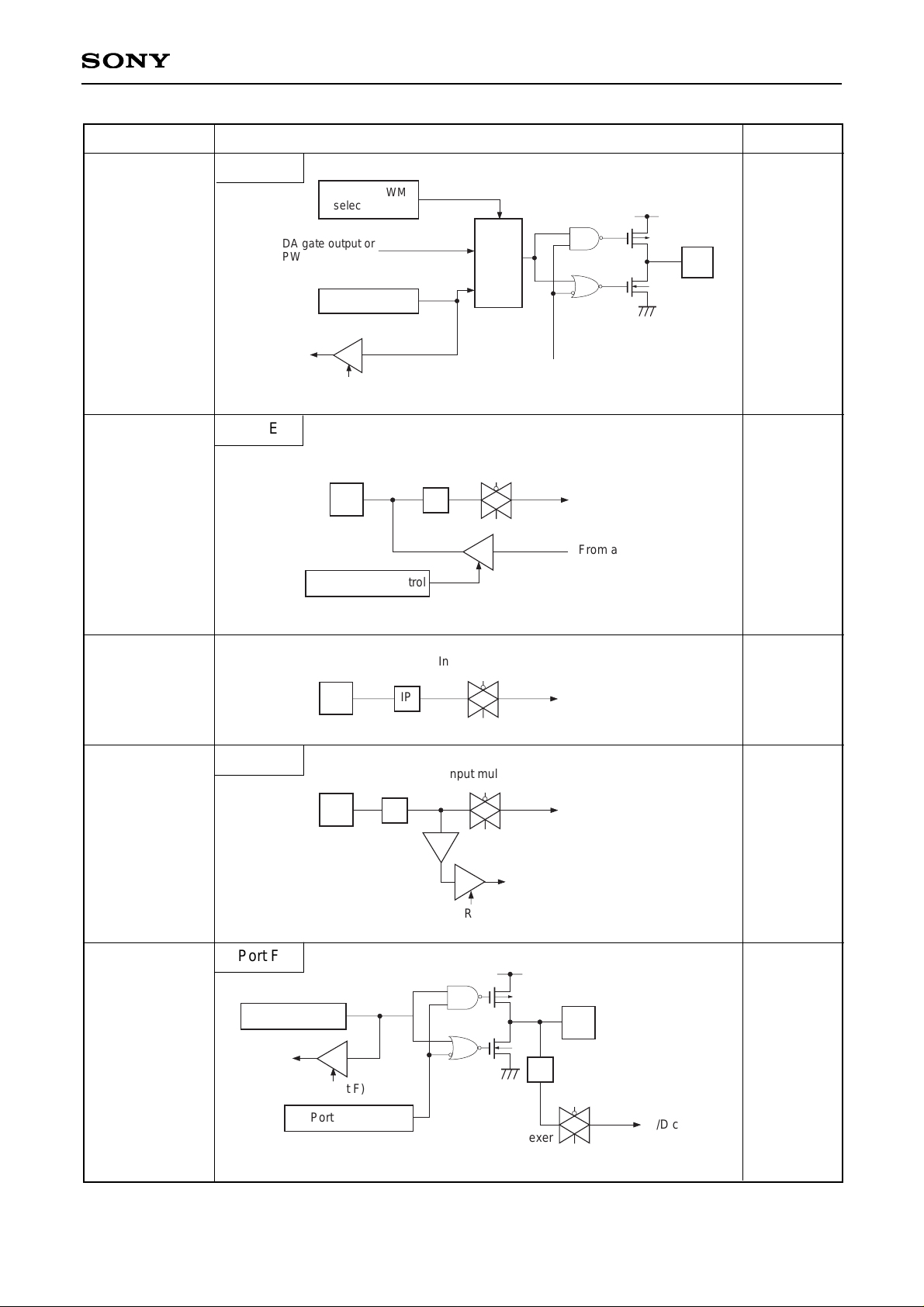
When reset
PE6/PWM0/
DAA0
PE7/PWM1/
DAA1
PF4/AN8
to
PF7/AN11
AN0/ANOUT
1 pin
3 pin
AN1
to
AN3
4 pins
High level
PFO/AN4
to
PF3/AN7
Port E
Pin
Circuit format
Port F data
IP
Data bus
RD (Port F)
Port/AD select
A/D converter
Input multiplexer
From amplifier circuit
IP
Input multiplexer
A/D converter
Analog output control
IP
Input multiplexer
A/D converter
Port E
Port F
RD (Port F)
Data bus
IP
Input multiplexer
A/D converter
Port F
DA gate output or
PWM output
Data bus
Port/DA/PWM
select
Port E data
RD (Port E)
MPX
Hi-Z control
 Loading...