

Sony CXP88160, CXP88152 Datasheet

CXP88152/88160
CMOS 8-bit Single Chip Microcomputer
Description
The CXP88152/88160 is a CMOS 8-bit microcomputer which consists of A/D converter, serial
interface, timer/counter, time base timer, high
precision timing pattern generation circuits, PWM
output, PWM for tuner, VISS/ VASS circuit, 32kHz
timer/counter, remote control receiving circuit,
fluorescent display panel (FDP) controller/driver,
VSYNC separator and the measurement circuit
which measure signals of capstan FG and drum
FG/PG and other servo systems, as well as basic
configurations like 8-bit CPU, ROM, RAM and I/O
port. They are integrated into a single chip.
Also, CXP88152/88160 provides sleep/stop
function which enables to lower power consumption
and ultra-low speed instruction mode in 32kHz
operation.
Features
• A wide instruction set (213 instructions) which cover various types of data
— 16-bit arithmetic/multiplication and division/boolean bit operation instructions
• Minimum instruction cycle 250ns at 16MHz operation
122µs at 32kHz operation
• Incorporated ROM capacity 52K bytes (CXP88152)
60K bytes (CXP88160)
• Incorporated RAM capacity 1296 bytes (including fluorescent display area)
• Peripheral function
— A/D converter 8 bits, 8 channels, successive approximation system
(Conversion time of 20µs/16MHz)
— Serial interface Incorporated 8-bit, 8-stage FIFO for data
(Auto transfer for 1 to 8 bytes), 1 channel
8-bit clock sync type, 1 channel
— Timer 8-bit timer/counter, 2 channels
19-bit time base timer
32kHz timer/counter
— High precision timing pattern generation PPG 8 pins 32-stage programmable circuit
RTG 5 pins, 2 channels
— PWM/DA gate output 12 bits, 2 channels (Repetitive frequency 62.5kHz/16MHz)
DA gate pulse output, 13 bits, 4 channels
— Servo input control Capstan FG, Drum FG/PG, CTL input
— VSYNC separator
— FRC capture unit Incorporated 26-bit and 8-stage FIFO
— PWM output 14-bit, 1 channel
— VISS/VASS circuit Pulse duty auto detection circuit
— 32kHz timer/event counter 32kHz oscillation circuit, ultra-low speed instruction mode
— Remote control reception circuit 8-bit pulse measurement counter, 6-stage FIFO
— Fluorescent display panel controller/driver Maximum 148-segment display possible
Hardware key scan function (Maximum 16 × 3 key matrix available)
Dimmer function
High voltage drive output (40V)
Incorporated pull-down resistor (Mask option)
— Tri-state output PPG 1 pin, RTG 1 pin, output 8 pins
— Pseudo HSYNC output function
— High speed head switching circuit
• Interruption 22 factors, 15 vectors, multi-interruption possible
• Standby mode SLEEP/STOP
• Package 100-pin plastic QFP
• Piggyback/evaluation chip CXP88100A 100-pin ceramic GFP
Sony reserves the right to change products and specifications without prior notice. This information does not convey any license by
any implication or otherwise under any patents or other right. Application circuits shown, if any, are typical examples illustrating the
operation of the devices. Sony cannot assume responsibility for any problems arising out of the use of these circuits.
Structure
Silicon gate CMOS IC
– 1 –
100 pin QFP (Plastic)
E95324-ST
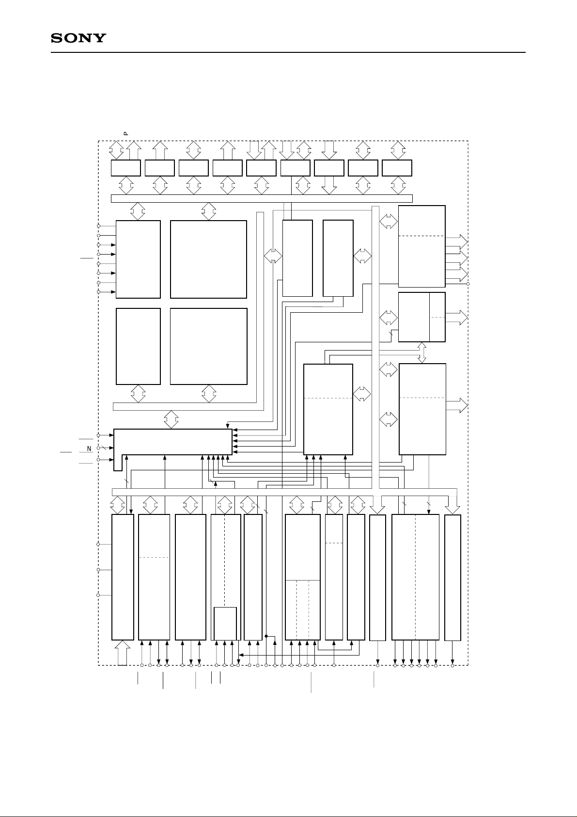
CXP88152/88160
Vss
V
DD
MP
RST
TX
TEX
XTAL
EXTAL
PA0 to PA7
4
4
PORT A
CLOCK
SPC700
PB0 to PB7
8
PORT B8PORT C
GENERATOR/
SYSTEM CONTROL
CPU CORE
PC0 to PC7
RAM
1296 BYTES
ROM
52K/60K BYTES
PD0 to PD7
PE0 to PE1
2
8
PORT D
PF0 to PF3
PE2 to PE7
4
6
PORT E
PRESCALER/
PF4 to PF7
PG0 to PG7
4
8
PORT F
PORT G3PORT H
32kHz
TIME BASE TIMER
TIMER/COUNTER
FIFO
PH0 to PH2
2
PI1 to PI7
7
PORT I
FDP
PULSE
REALTIME
RAM
8
8
/DRIVER
8
CONTROLLER
1
CH
5
CH0
GENERATOR
RAM
8
FDP
T15/S8
T8/S15
V
S0 to S7
to
T0 to T7
RTO3 to RTO7
PPO0 to PPO7
INT2
INT1/NMI
INT0
AVss
REF
AV
AV
DD
2
2
A/D CONVERTER
8
AN0 to AN7
FIFO
(CH0)
SERIAL
INTERFACE UNIT
SI0
CS0
SO0
SCK0
INTERRUPT CONTROLLER
2
(CH1)
8 BIT TIMER/COUNTER1
8 BIT TIMER/COUNTER 0
SERIAL INTERFACE UNIT
V SYNC SEPARATOR
EC
SELECT
SI1
SO1
SCK1
EC0
EC1
EC2
SYNC0/EC2
TO/DDO/ADJ
2
2
EXI0
SYNC1
EXI1
ADJ
3
CONTROL
SERVO INPUT
CTL
DRUM
CAPSTAN
DFG
CFG
DPG
PBCTL
FRC
CAPTURE UNIT
FIFO
VISS/VASS
REMOCON INPUT
RMC
PATTERN
GENERATOR
PROGRAMABLE
2
4
14 BIT PWM GENERATOR
PWM
PWM0
12 BIT PWM GENERATOR CH1
12 BIT PWM GENERATOR CH0
DAB1
DAA1
DAB0
DAA0
PWM1
PSEUDO HSYNC GENERATOR
HGO
Block Diagram
– 2 –
Pin Configuration (Top View)
PB1
PB2
PB3
PB4
PB5
PB6
PB7
PH1/KR1
PH0/KR0
NC
PH2/KR2
CXP88152/88160
SS
DD
V
TX
V
TEX
PI2/PWM
PI1/RMC
PI5/SCK0
PI4/INT1/NMI/CS0
PI3/TO/DDO/ADJ
PB0
PC7/RTO7
PC6/RTO6
PC5/RTO5
PC4/RTO4
PC3/RTO3
PC2
PC1
PC0
PA7/PPO7
(HAMP) PA6/PPO6
(ROTA) PA5/PPO5
(RF-PLS) PA4/PPO4
PA3/PPO3
PA2/PPO2
PA1/PPO1
HGO/PA0/PPO0
PF7
SI1/PF6
SO1/PF5
SCK1/PF4
PF3/AN7
PF2/AN6
PF1/AN5
PF0/AN4
AN3
AN2
AVREF
AVSS
AVDD
10
12
13
14
15
16
17
18
19
20
23
25
29
30
11
21
22
24
26
27
28
100
99
98
1
2
3
4
5
6
7
8
9
32
31
33
97
34
96
35
95
36
94
37
93
38
92
39
91
40
90
41
89
42
88
43
87
44
45
86
85
46
84
47
83
48
82
49
50
81
80
79
78
77
76
75
74
73
72
71
70
69
68
67
66
65
64
63
62
61
60
59
58
57
56
55
54
53
52
51
PI6/SO0
PI7/SI0
VFDP
PD0/S0
PD1/S1
PD2/S2
PD3/S3
PD4/S4
PD5/S5
PD6/S6
PD7/S7
S8/T15
S9/T14
S10/T13
S11/T12
S12/T11
S13/T10
S14/T9
S15/T8
T7
T6
T5
T4
T3
T2
T1
T0
PE0/INT0 (ENV-DET)
PE1/EC0/INT2
PWM0/PE2
SS
MP
AN1
AN0
PG6/EXI0
PG7/EXI1
PG5/SYNC1
PG3/PBCTL/EC1
PG4/SYNC0/EC2
PG2/DPG
RST
V
XTAL
EXTAL
Note) 1. NC (Pin 90) is always connected to VDD.
2. Vss (Pins 41 and 88) are both connected to GND.
3. MP (Pin 39) must be connected to GND.
– 3 –
PG0/CFG
PG1/DFG
PE5/DAA1
DAB0/PE6
DAB1/PE7
PE4/DAA0
PE3/PWM1
Pin Description
Symbol I/O Description
CXP88152/88160
PA0/PPO0/
HGO
PA1/PPO1
PA2/PPO2
PA3/PPO3
PA4/PPO4
PA5/PPO5
PA6/PPO6
PA7/PPO7
PB0 to PB7
PC0 to PC2
PC3/PPO3
to
PC7/PPO15
T0 to T7
T8/S15
to
T15/S8
Output/Real time
output/Output
I/O/
Real time output
Output/
Real time output
Output
I/O
I/O/
Real time output
Output
Output/Output
Pseudo HSYNC
(Port A)
PA0 and PA5 to PA7 are
for putputs; PA1 to PA4
are for I/O. I/O can be set
in a unit of single bits.
output pin.
Real-time pulse generator (RTG) output.
Functions as high precision real-time
pulse output port.
(5 pins)
Data is gated with RTO
content by OR-gate and
they are output.
(8 pins)
Head switching
output pins.
(2 pins)
8-bit output port. Tri-state can be controlled.
(8 pins)
(Port C)
8-bit I/O port. I/O can be
set in a unit of single bits.
Data is gated with RTO
content by OR-gate and
Real-time pulse generator (RTG) output.
Functions as high precision real-time pulse
output port.
(5 pins)
they are output. (8 pins)
FDP timing signal output pin. (8 pins)
Output pins for FDP timing signal and segment signal. (8 pins)
PD0/S0
to
PD7/S7
PE0/INT0
PE1/EC0/
INT2
PE2/PWM0
PE3/PWM1
PE4/DAA0
PE5/DAA1
PE6/DAB0
PE7/DAB1
AN0 to AN3
PF0/AN4
to
PF3/AN7
PF4/SCK1
PF5/SO1
PF6/SI1
PF7
Output/Output
Input/Input
Input/Input/Input
Output/Output
Output/Output
Output/Output
Output/Output
Output/Output
Output/Output
Input
Input/Input
I/O/I/O
I/O/Output
I/O/Input
I/O
(Port D)
8-bit output port.
FDP segment signal output pin. (8 pins)
(8 pins)
Trigger pulse
input pin for head
switching output.
External event
(Port E)
8-bit port.
Lower 2 bits are for
inputs; upper 6 bits are for
outputs.
input pin for
timer/counter.
PWM output pins.
(2 pins)
(8 pins)
DA gate pulse output pins.
(4 pins)
Analog input pins to A/D converter. (8 pins)
(Port F)
Lower 4 bits are for
inputs; upper 4 bits are
for I/O. I/O can be set
in a unit of single bits.
(8 pins)
Serial clock (CH1) I/O pin.
Serial data (CH1) output pin.
Serial data (CH1) input pin.
Input pin to request
external interruption.
Active when falling edge.
Input pin to request
external interruption.
Active when falling edge.
– 4 –
Symbol I/O Description
PG0/CFG
Input/Input
Capstan FG input pin.
CXP88152/88160
PG1/DFG
PG2/DPG
PG3/
PBCTL/EC1
PG4/
SYNC0/EC2
PG5/SYNC1
PG6/EXI0
PG7/EXI1
PH0/KR0
to
PH2/KR2
PI1/RMC
PI2/PWM
PI3/TO/
DDO/ADJ
PI4/INT1/
NMI/CS0
PI5/SCK0
Input/Input
Input/Input
Input/Input/Input
Input/Input/Input
Input/Input
Input/Input
Input/Input
I/O/Input
I/O/Input
I/O/Input
I/O/Input
I/O/Input/
Input/Input
I/O/I/O
(Port G)
8-bit input port.
(8 pins)
(Port H)
3-bit I/O port.
(3 pins)
(Port I)
7-bit I/O port.
I/O can be set
in a unit of
single bits.
(7 pins)
Drum FG input pin.
Drum PG input pin.
External event
Playback CTL input pin.
input pin for
timer/counter.
External event
input pin for
Composite sync signal input pin.
timer/counter.
External input pin for FRC capture unit.
Key return input signal for key scanning at FDP
segment signal. (3 pins)
Remote control reception circuit input pin.
14-bit PWM output pin.
Timer/counter, CTL duty detection, 32kHz oscillation
adjustment output pin.
Input pin to request external interruption,
non-maskable interruption and for serial chip select
(CH0). Active when falling edge.
Serial clock (CH1) I/O pin.
PI6/SO0
PI7/SI0
EXTAL
XTAL
TEX
TX
RST
MP
VFDP
AVDD
AVREF
AVss
VDD
Vss
NC
I/O/Output
I/O/Input
Input
Output
Input
Output
Input
Input
Input
Serial data (CH1) output pin.
Serial data (CH1) input pin.
Connecting pin of crystal oscillator for system clock.
When supplying the external clock, input the external clock to EXTAL
pin and input opposite phase clock to XTAL pin.
Connecting pin of crystal oscillator for 32kHz timer clock.
When used as event counter, input to TEX pin and leave TX pin open.
(In this time, feedback resistor is not removed.)
System reset pin of active “L” level.
Test mode pin. Always connect to GND.
FPD voltage supply pin when specifying internal resistor by mask
option.
Positive power supply pin of A/D converter.
Reference voltage input pin of A/D converter.
GND pin of A/D converter.
Positive power supply pin.
GND pin. Connect both Vss pins to GND.
Not connected. Under normal operation, connect to VDD.
– 5 –
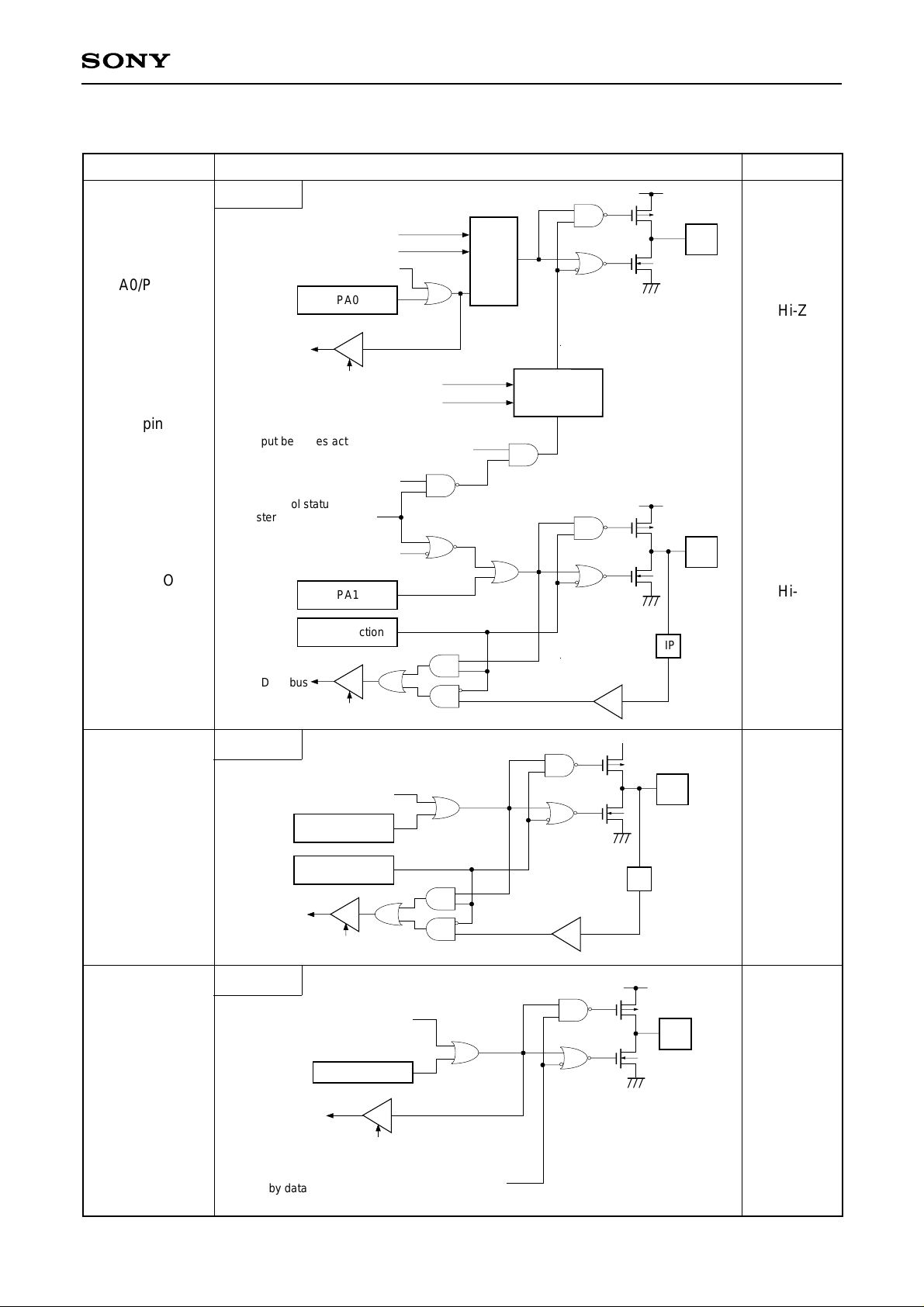
I/O Circuit Format for Pins
CXP88152/88160
Pin
PA0/PPO0/
HGO
1 pin
PA1/PPO1
Circuit format
Port A
HSEL
HOUT
PPO0
PA0
Data bus
RD
(Port A)
Output becomes active from high impedance
by data writing to port register.
PPG control status
register bit 0
Tri-state control selection
PA1
HSEL
HOUTE
PPO1
PPO1
When reset
MPX
Hi-Z
MPX
Hi-Z
1 pin
PA2/PPO2
to
PA4/PPO4
3 pins
PA5/PPO5
to
PA7/PPO7
Data bus
Port A
Data bus
Port A
Port A direction
Data bus
PA1 direction
IP
RD (Port A)
PPO data
Port A data
Hi-Z
IP
RD (Port A)
PPO data
Port A data
Hi-Z
3 pins
RD (Port A)
Output becomes active from high impedance
by data writing to port register.
– 6 –
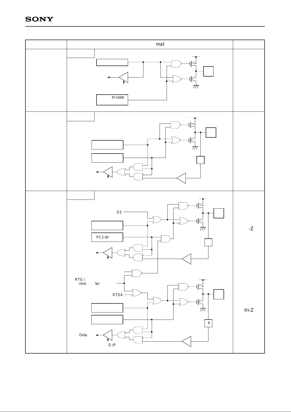
CXP88152/88160
PB0
to
PB7
8 pins
PC0
to
PC2
3 pins
Port B
Port C
Data bus
Port B data
Data bus
Port B tri-state
control
Port C data
Port C direction
RD (Port C)
Circuit format
RD (Port B)
When resetPin
Hi-Z
Hi-Z
IP
PC3/RTO3
1 pin
PC4/RTO4
Port C
RTO3
PC3
PC3 direction
Data bus
RD (Port C)
RTG interruption
control register bit 7
Tri-state control selection
PC4
PC4 direction
Data bus
Hi-Z
IP
RTO4
RTO4
Hi-Z
IP
1 pin
RD (Port C)
– 7 –
CXP88152/88160
PC5/RTO5
to
PC7/RTO7
3 pins
PD0/S0
to
PD7/S7
8 pins
Port C
Port C data
Port C direction
Data bus
RD (Port C)
Port D
Segment output data
Output selection control signal
("0" when reset)
Port D data
Data bus
RD (Port D)
RTO data
Circuit format
Pull-down resistor
High voltage drive
transistor
Mask option
OP
When resetPin
Hi-Z
IP
Hi-Z or Low
level (when
PD resistor is
connected)
VFDP
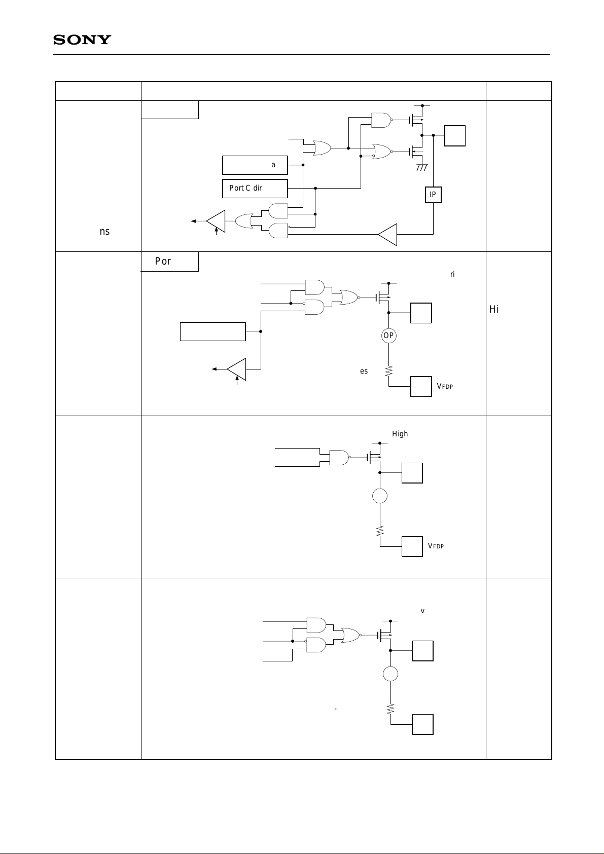
T0 to T7
8 pins
T8/S15
to
T15/S8
8 pins
Timing output data
Output selection control signal
("0" when reset)
Timing output data
Output selection control signal
("0" when reset)
Segment output data
Pull-down resistor
Pull-down resistor
High voltage drive
transistor
Mask option
OP
High voltage drive
transistor
Mask option
OP
Hi-Z or Low
level (when
PD resistor is
connected)
VFDP
Hi-Z or Low
level (when
PD resistor is
connected)
VFDP
– 8 –
 Loading...