

Sony CXP82324, CXP82320, CXP82316 Datasheet

CXP82316/82320/8232
4
CMOS 8-bit Single Chip Microcomputer
Description
The CXP82316/82320/82324 microcomputer is
composed of a CPU, ROM and RAM, and I/O ports.
These chips feature many other high-performance
circuits in a single-chip CMOS design, including an
A/D converter, serial interface, timer/counter, timebase timer, capture timer/counter, fluorescent display
controller/driver, remote control receiver.
This device also includes a power-on reset function
and sleep/stop functions which can be used to
achieve low power consumption.
Features
• Instruction set which supports a wide array of data types
— 213 types of instructions which include 16-bit calculations, multiplication and division arithmetic, and
boolean bit operations.
• Minimum instruction cycle 400ns for 10MHz operation
• On-chip ROM 16K bytes (CXP82316)
20K bytes (CXP82320)
24K bytes (CXP82324)
• On-chip RAM 704 bytes (Including fluorescent display data area)
• Peripheral functions:
— A/D converter 8-bit, 8-channel, successive approximation system
(conversion rate 32µs/10MHz)
— Serial interface On-chip 8-bit, 8-stage FIFO (1 to 8 bytes auto transfer) 1 channel
8-bit clock synchronized 1 channel
— Timers 8-bit timer
8-bit timer/counter
19-bit time-base timer
16-bit capture timer/counter
— Fluorescent display controller/driver
Maximum of 336 segment display available
1 to 16 digits dynamic display
Dimmer function
High voltage tolerant output (40V)
On-chip pull-down resistor (Mask option)
— Remote control receiver circuit
On-chip noise elimination circuit
On-chip 6 stage FIFO 8-bit pulse measurement counter
• Interrupts 14 factors, 15 vectors multi-interruption possible
• Standby mode Sleep/stop
• Package 80-pin plastic QFP
• Piggyback/evaluator CXP82300 80-pin ceramic QFP
80 pin QFP (Plastic)
Structure
Silicon gate CMOS IC
Sony reserves the right to change products and specifications without prior notice. This information does not convey any license by
any implication or otherwise under any patents or other right. Application circuits shown, if any, are typical examples illustrating the
operation of the devices. Sony cannot assume responsibility for any problems arising out of the use of these circuits.
– 1 –
E91722B78-PS
CXP82316/82320/82324
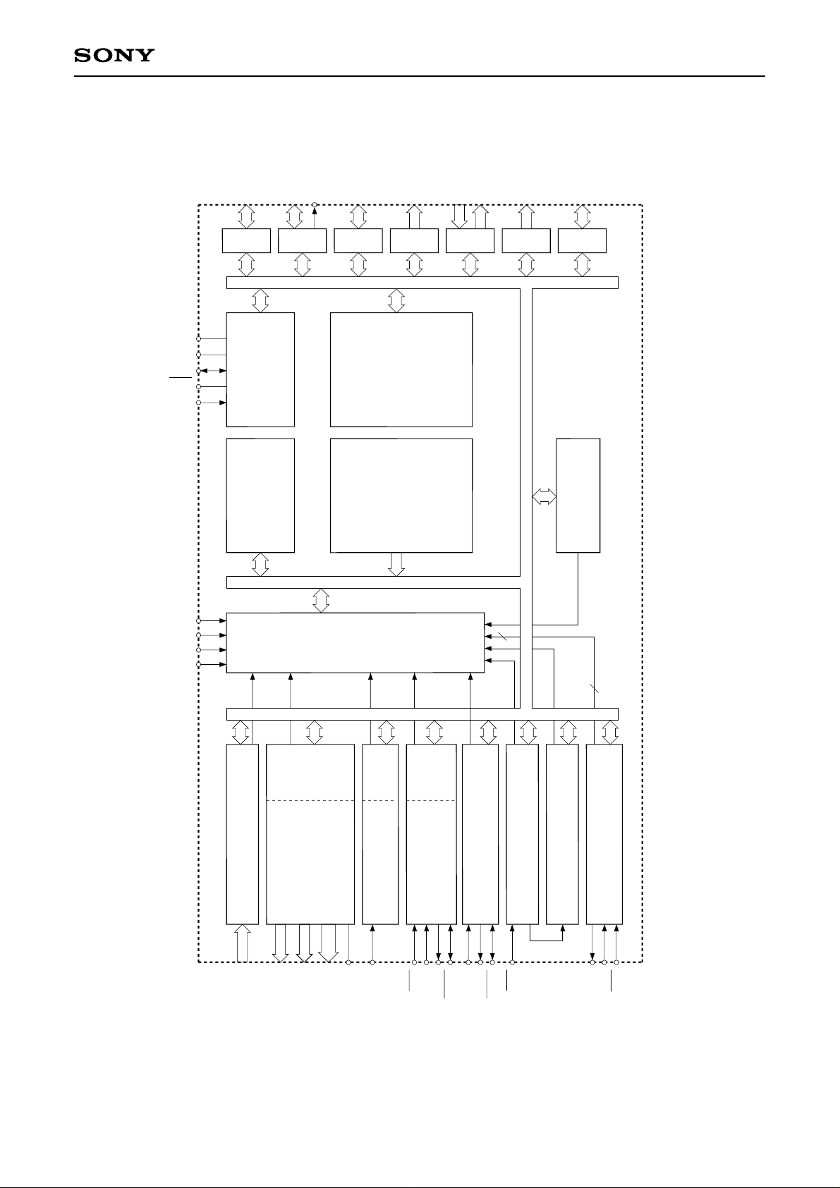
SS
V
V
DD
RST
XTAL
EXTAL
PA0 to PA7
8
PB0 to PB6
PB7
7
PORT A
CLOCK GEN./
SYSTEM CONTROL
SPC700
CPU CORE
PORT B
PC0 to PC7
8
PORT C
RAM
704 BYTES
ROM
16K/20K/24K BYTES
PD0 to PD7
8
PE0 to PE5
6
PORT D
PE6 to PE7
2
PF0 to PF7
8
PORT E
PORT F
PRESCALER/
PG0 to PG3
4
PORT G
TIME BASE TIMER
Block Diagram
INT3
INT2
INT1
INT0
RAM
80 BYTES
A/D CONVERTER
FDP
CONTROLLER/
8
8
8
T8/S28
T15/S21
T0 to T7
AN0 to AN7
DRIVER
21
FDP
V
S0 to S20
FIFO
REMOCON
RMC
INTERRUPT CONTROLLER
2
FIFO
UNIT 0
SERIAL
INTERFACE
SI0
CS0
SO0
SCK0
SERIAL INTERFACE UNIT 1
SI1
SO1
8 BIT TIMER/COUNTER 0
EC0
SCK1
2
8 BIT TIMER 1
16 BIT CAPTURE
TIMER/COUNTER 2
TO
EC1
CINT
– 2 –
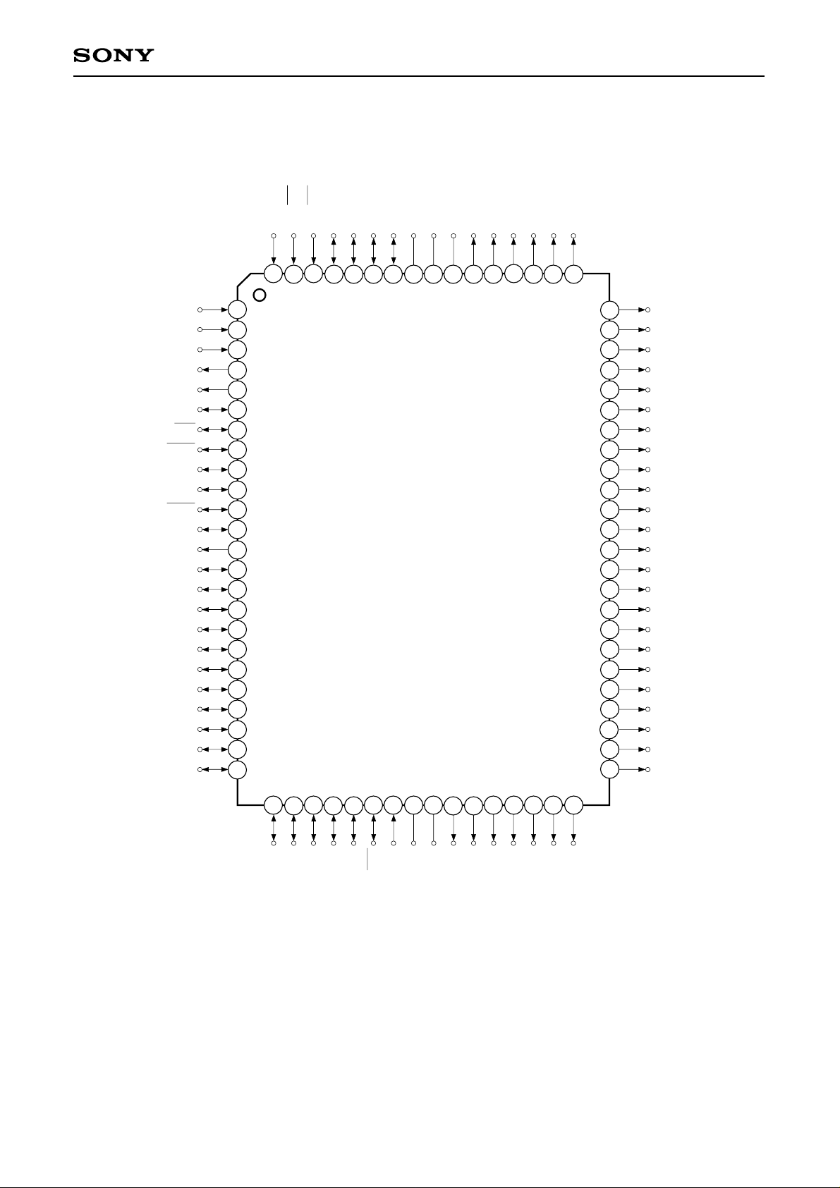
Pin Assignment (Top View)
PE1/EC1/INT1
PE2/IN2
PE0/EC0/INT0
PG3
PG2
PG1
PG0
NC
DD
V
FDP
V
T0
T1
T2
T3
T4
CXP82316/82320/82324
T5
PE3/INT3
PE4/RMC
PE5
PE6
PE7/TO
PB0/CINT
PB1/CS0
PB2/SCK0
PB3/SI0
PB4/SO0
PB5/SCK1
PB6/SI1
PB7/SO1
PC0/KR0
PC1/KR1
PC2/KR2
PC3/KR3
PC4/KR4
PC5/KR5
PC6/KR6
PC7/KR7
PA0/AN0
PA1/AN1
PA2/AN2
10
11
12
13
14
15
16
17
18
19
20
21
22
23
24
80
78
79
1
2
3
4
5
6
7
8
9
77
76
75
74
73
72
71
70
69
68
67
66
65
55
47
45
44
64
63
62
60
59
58
57
56
54
53
52
51
50
49
48
46
43
42
41
61
T6
T7
T8/S28
T9/S27
T10/S26
T11/S25
T12/S24
T13/S23
T14/S22
T15/S21
S20
S19
S18
S17
S16
PF7/S15
PF6/S14
PF5/S13
PF4/S12
PF3/S11
PF2/S10
PF1/S9
PF0/S8
PD7/S7
25
26
PA3/AN3
27
28
PA4/AN4
PA5/AN5
29
PA7/AN7
PA6/AN6
30
31
RST
32
XTAL
EXTAL
33
SS
V
34
Note) NC (Pin 73) is always connected to VDD.
– 3 –
35
PD1/S1
PD0/S0
36
PD2/S2
37
PD3/S3
38
PD4/S4
39
PD5/S5
40
PD6/S6

Pin Description
Symbol I/O Description
CXP82316/82320/82324
PA0/AN0
to
PA7/AN7
PB0/CINT
PB1/CS0
PB2/SCK0
PB3/SI0
PB4/SO0
PB5/SCK1
PB6/SI1
PB7/SO1
PC0/KR0
to
PC7/KR7
PE0/INT0/EC0
PE1/INT1/EC1
PE2/INT2
PE3/INT3
PE4/RMC
PE5
PE6
I/O/Analog input
I/O/Input
I/O/Input
I/O/I/O
I/O/Input
I/O/Output
I/O/I/O
I/O/Input
Output/Output
I/O/Input
Input/Input/Input
Input/Input/Input
Input/Input
Input/Input
Input/Input
Input
Output
(Port A)
8-bit port; single bit
addressable.
(8 pins)
(Port B)
Single bit addressable from
amongst lower 7 bits;
highest bit (PB7)
dedicated to output.
(8 pins)
(Port C)
8-bit port; single bit
addressable. Can provide
12mA sink current.
(8 pins)
(Port E)
8-bit port with lower 6 bits
dedicated to input and
upper 2 bits dedicated to
output.
(8 pins)
Analog inputs to A/D converter.
(8 pins)
External capture input to 16-bit timer/counter.
Chip select input for serial interface (CH0).
Serial clock (CH0) input/output.
Serial data (CH0) input.
Serial data (CH0) output.
Serial clock (CH1) input/output.
Serial data (CH1) input.
Serial data (CH1) output.
Key return input for FDP segment signal.
which performs key scanning.
External event input
to timer/counter.
Input for external
(2 pins)
interrupt requests.
(4 pins)
Input for remote control receiver circuit.
PE7/TO
PG0 to PG3
PF0/S8
to
PF7/S15
S16 to S20
T8/S28
to
T15/S21
T0 to T7
PD0/S0
to
PD7/S7
Output/Output
I/O
Output/Output
Output
Output/Output
Output
Output/Output
Output pin for 16-bit timer/counter
rectangular waveform.
(Port G)
4-bit input/output port; single bit addressable.
(4 pins)
(Port F)
8-bit dedicated output port.
(8 pins)
Segment signal
output for FDP.
Segment signal output for FDP.
Dual purpose output for FDP timing and segment signals.
Timing signal output for FDP.
(Port D)
8-bit dedicated output port.
Segment signal output for FDP.
(8 pins)
– 4 –

Symbol I/O Description
CXP82316/82320/82324
VFDP
EXTAL
XTAL
RST
NC
VDD
VSS
Input
Output
I/O
Provides voltage for FDP when on-chip resistor is selected under mask
option.
Connection for system clock oscillation crystal. When using an external
clock, input normal signal to EXTAL and reverse phase signal to the
XTAL pin.
System reset, active "L". The RST pin is an input/output pin which
outputs a "L" level from the on-chip power on reset circuit when the
power is turned on. (Mask option)
NC pin is always connected to VDD.
Positive power supply pin.
GND
– 5 –

Input/Output Circuit Formats for Pins
CXP82316/82320/82324
Pin
PA0/AN0
to
PA7/AN7
8 pins
PB0/CINT
PB1/CS0
PB3/SI0
PB6/SI1
Port A
Port B
Data bus
Data bus
Port A data
Port A detection
"0" when reset
RD (Port A)
Port A input select
"0" when reset
Port B data
Port B direction
"0" when reset
Circuit format
Input multiplexer
A/D converter
Schmitt input
IP
When reset
Input
protection
circuit
Hi-Z
IP
Hi-Z
4 pins
PB2/SCK0
PB5/SCK1
2 pins
Port B
Port B output select
"0" when reset
"0" when reset
Data bus
SCK OUT
Output enable
Port B data
Port B direction
RD (Port B)
SCK in
RD (Port B)
CINT
CS0
SI0
SI1
IP
Hi-Z
Schmitt input
– 6 –
 Loading...