

Sony CXP82060, CXP82052, CXP82040, CXP82032 Datasheet

CMOS 8-bit Single Chip Microcomputer
Description
The CXP82032/82040/82052/82060 is a CMOS 8bit single chip microcomputer integrating on a single
chip an A/D converter, serial interface, timer/counter,
time-base timer, capture timer/counter, fluorescent
display panel controller/driver, remote control
reception circuit, and PWM output besides the basic
configurations of 8-bit CPU, ROM, RAM, and I/O port.
The CXP82032/82040/82052/82060 also provides
sleep/stop function that enables lower power
consumption.
Features
• Wide-range instruction system (213 instructions)
to cover various types of data
— 16-bit arithmetic/multiplication and division/boolean bit operation instructions
• Minimum instruction cycle 250ns at 16MHz operation
122µs at 32kHz operation
• Incorporated ROM capacity 32k bytes (CXP82032)
40k bytes (CXP82040)
52K bytes (CXP82052)
60K bytes (CXP82060)
• Incorporated RAM capacity 3984 bytes (including fluorescent display area)
• Peripheral functions
— A/D converter 8 bits, 8 channels, successive approximation method
(Conversion time of 3.25µs/16MHz)
— Serial interface Buffer RAM incorporated (Auto transfer for 1 to 32 bytes), 1 channel
8-bit clock synchronized type (MSB/LSB first selectable), 1 channel
Start-stop synchronized type (UART), 1 channel
— Timers 8-bit timer, 8-bit timer/counter, 19-bit time-base timer
16-bit capture timer/counter, 32kHz timer/counter
—
Fluorescent display panel controller/driver
Supports the universal grid fluorescent display panel.
High voltage drive output port of 56 pins (40V)
Maximum of 640 segments display possible
Display timing number of 1 to 20
Dimmer function
Incorporated pull-down resistor (Mask option)
Hardware key scan function (Maximum of 16 × 8 key matrix
supportable)
— Remote control reception circuit 8-bit pulse measurement counter, 6-stage FIFO
— PWM output 14 bits, 1 channel
• Interruption 17 factors, 15 vectors, multi-interruption possible
• Standby mode Sleep/stop
• Package 100-pin plastic QFP
• Piggy/evaluation chip CXP82000 100-pin ceramic QFP
– 1 –
E97413A95-PS
Sony reserves the right to change products and specifications without prior notice. This information does not convey any license by
any implication or otherwise under any patents or other right. Application circuits shown, if any, are typical examples illustrating the
operation of the devices. Sony cannot assume responsibility for any problems arising out of the use of these circuits.
CXP82032/82040/82052/82060
100 pin QFP (Plastic)
Structure
Silicon gate CMOS IC
– 2 –
CXP82032/82040/82052/82060
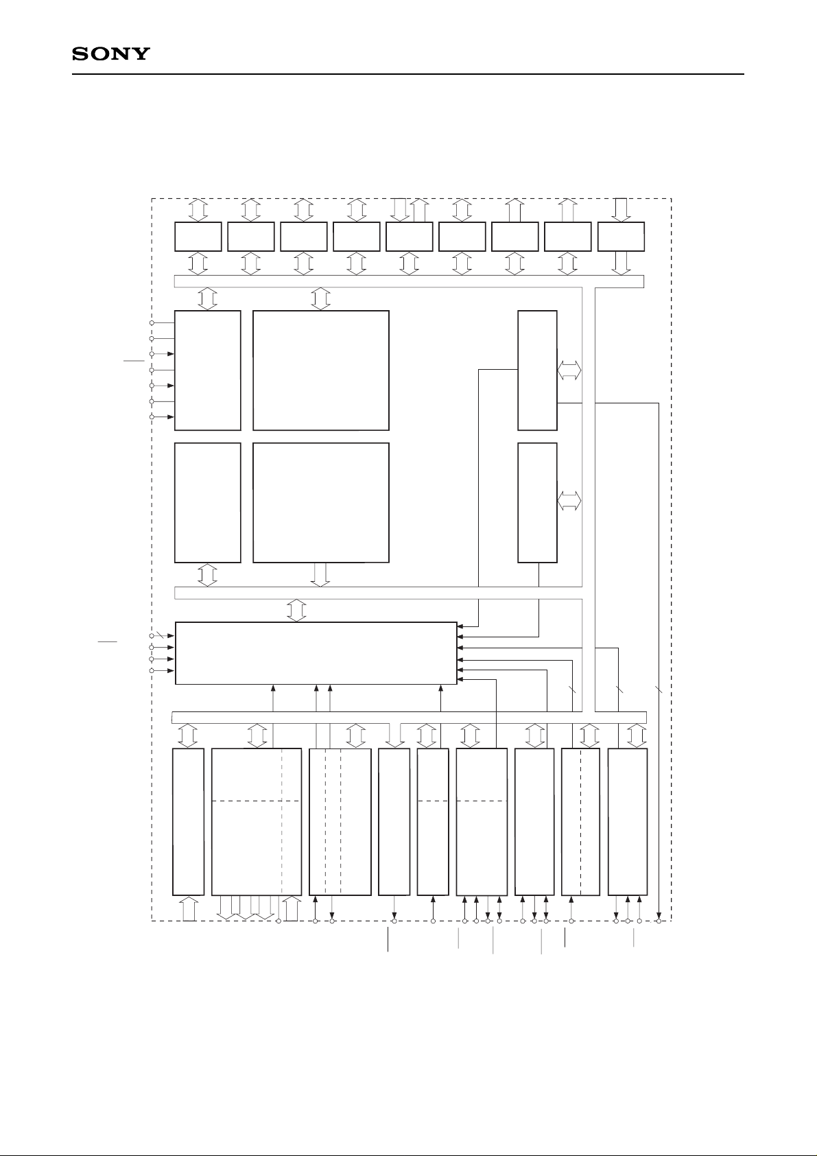
8-BIT TIMER/COUNTER 0
8-BIT TIMER 1
UART BAUD RATE
GENERATOR
UART RECEIVER
UART TRANSMITTER
INT2
XTAL
PWM
RAM
3984
BYTES
SPC 700
CPU CORE
A/D CONVERTER
INT3/NMI
INT1
INT0
AN0 to AN7
8
PA0 to PA7
FDP
CONTROLLER/
DRIVER
32kHz
TIMER/COUNTER
PRESCALER/
TIME-BASE TIMER
RST
V
DD
V
SS
PORT A
PORT B
PORT C
PORT D
PORT E
PORT F
PORT G
8
8
6
2
8
8
8
8
PB0 to PB7
PC0 to PC7
PD0 to PD7
PE0 to PE5
PF0 to PF7
PG0 to PG7
PE6 to PE7
TEX
EXTAL
TX
CS0
2
ROM
32K/40K/ 52K/60K
BYTES
RAM
KEY SCAN
PORT H
PH0 to PH7
8
CLOCK GENERATOR/
SYSTEM CONTROL
14-BIT PWM GENERATOR
FIFOREMOCON
RMC
SI0
SO0
SCK0
SI1
SO1
SCK1
EC0
TO
CINT
EC1
ADJ
G0/A0 to G15/A15
A16 to A23
A24 to A56
V
FDP
KR0 to KR7
16
8
32
8
2
SERIAL INTERFACE (CH1)
16-BIT CAPTURE
TIMER/COUNTER 2
SERIAL
INTERFACE
(CH0)
BUFFER
RAM
2
2
PORT I
PI0 to PI4
4
TxD
RxD
INTERRUPT CONTROLLER
RAM
Block Diagram
– 3 –
CXP82032/82040/82052/82060
Pin Assignment (Top View)
G1/A1
G0/A0
NC
PE0/EC0/INT0
PE1/EC1/INT1
PE2/INT2
PE3/INT3/NMI
PE4/RMC
PE5/CINT
PE6/PWM
PE7/TO/ADJ
PC0/KR0
PC1/KR1
PC2/KR2
PC3/KR3
PC4/KR4
PC5/KR5
PC6/KR6
PC7/KR7
PB0/TxD
PB1/CS0/RxD
PB2/SCK0
PB3/SI0
PB4/SO0
PB5/SCK1
PB6/SI1
PB7/SO1
PI0
PA0/AN0
PA1/AN1
2
3
4
5
6
7
8
9
10
11
12
13
14
15
16
17
18
19
20
21
22
23
24
25
26
27
28
29
30
40
39
38
37
36
35
34
31
32
33
41
42
43
44
45
46
47
48
49
50
51
52
53
54
55
56
57
58
59
60
70
69
68
67
63
64
65
66
61
62
71
72
73
74
81
82
83
84
75
76
77
78
88
87
86
85
79
80
89
90
100
99
98
97
96
95
94
91
92
93
1
PA2/AN2
PA3/AN3
PA4/AN4
PA5/AN5
PA6/AN6
PA7/AN7
PI1
RST
EXTAL
XTAL
Vss
PI2/TX
PI3/TEX
V
DD
V
FDP
PD0/A55
PD1/A54
PD2/A53
PD3/A52
PD4/A51
A21
A22
A23
PH7/A24
PH6/A25
PH5/A26
PH4/A27
PH3/A28
PH2/A29
PH1/A30
PH0/A31
PG7/A32
PG6/A33
PG5/A34
PG4/A35
PG3/A36
PG2/A37
PG1/A38
PG0/A39
PF7/A40
PF6/A41
PF5/A42
PF4/A43
PF3/A44
PF2/A45
PF1/A46
PF0/A47
PD7/A48
PD6/A49
PD5/A50
G2/A2
G3/A3
G4/A4
G5/A5
G6/A6
G7/A7
G8/A8
G9/A9
G10/A10
G11/A11
G12/A12
V
DD
G13/A13
G14/A14
G15/A15
A16
A17
A18
A19
A20
Note) 1. NC (Pin 3) is left open.
2. VDD (Pins 44 and 89) must be connected to VDD.

– 4 –
CXP82032/82040/82052/82060
Pin Description
Symbol I/O
Functions
I/O/
Analog input
PA0/AN0
to
PA7/AN7
(Port A)
8-bit I/O port. I/O can be set in a
unit of single bits. Incorporation
of the pull-up resistor can be set
through the program in a unit of
4 bits.
(8 pins)
Analog inputs to A/D converter.
(8 pins)
I/O/Input
PC0/KR0
to
PC7/KR7
PE0/INT0/
EC0
PE1/INT1/
EC1
PE2/INT2
PE3/INT3/
NMI
PE4/RMC
PE5/CINT
PE6/PWM
PE7/TO/
ADJ
Input/Input/
Input
Input/Input/
Input
Input/Input
Input/Input/
Input
Input/Input
Input/Input
Output/Output
Output/Output/
Output
(Port C)
8-bit I/O port. I/O can be set in a
unit of single bits. Can drive
12mA sink current.
Incorporation of the pull-up
resistor can be set through the
program in a unit of 4 bits.
(8 pins)
Serves as key return inputs when
operating key scan with fluorescent
display panel (FDP) segment signal.
(8 pins)
I/O/Output
PD0/A55
to
PD7/A48
(Port D)
8-bit I/O port. I/O can be set in a
unit of single bits.
(8 pins)
FDP segment signal (anode
connection) outputs.
(Port E)
8-bit port. Lower 6 bits are for
inputs; upper 2 bits are for
outputs.
(8 pins)
External event inputs
for timer/counter.
(2 pins)
Inputs for
external
interruption
request.
(4 pins)
Non-maskable
interruption request input.
Remote control reception circuit input.
External capture input to 16-bit
timer/counter.
14-bit PWM output.
Output for the 16-bit timer/counter
rectangular waves, and 32kHz
oscillation frequency division.
I/O/Output
I/O/Input/
Input
I/O/I/O
I/O/Input
I/O/Output
I/O/I/O
I/O/Input
I/O/Output
PB0/TxD
PB1/CS0/
RxD
PB2/SCK0
PB3/SI0
PB4/SO0
PB5/SCK1
PB6/SI1
PB7/SO1
(Port B)
8-bit I/O port. I/O can be set in a
unit of single bits. Incorporation
of the pull-up resistor can be set
through the program in a unit of
4 bits.
(8 pins)
UART transmission data output.
Serial clock I/O (CH0).
Serial data input (CH0).
Serial data output (CH0).
Serial clock I/O (CH1).
Serial data input (CH1).
Serial data output (CH1).
Chip select input
for serial interface
(CH0).
UART reception
data input pin.

– 5 –
CXP82032/82040/82052/82060
(Port F)
8-bit I/O port. I/O can be set in a
unit of single bits.
(8 pins)
FDP segment signal (anode
connection) outputs.
(8 pins)
Symbol
I/O
Functions
OutputA16 to A23
FDP segment signal (anode connection) outputs.
(8 pins)
Output/Output
G0/A0
to
G15/A15
Outputs for FDP timing signals (grid connection)/segment signals (anode
connection).
(16 pins)
Output/Output
Input
Input
Input
Input/Input
PH0/A31
to
PH7/A24
PI0
PI1
PI2/TX
PI3/TEX
Output/Output
PG0/A39
to
PG7/A32
(Port H)
8-bit output port.
(8 pins)
(Port I)
4-bit input port.
(4 pins)
VFDP
EXTAL
XTAL
RST
NC
VDD
VSS
Input
Input
FDP voltage supply when incorporated pull-down (PD) resistor is set by
mask option.
Crystal connectors for system clock oscillation. When the clock is
supplied externally, input to EXTAL; opposite phase clock should be
input to XTAL.
Low-level active, system reset.
NC. Under normal operation, leave this pin open.
VCC supply.
GND.
FDP segment signal (anode
connection) outputs.
(8 pins)
Crystal connectors for 32kHz timer/counter clock
oscillation. For usage as event counter, input to TEX,
and leave TX open.
(Port G)
8-bit output port.
(8 pins)
FDP segment signal (anode
connection) outputs.
(8 pins)
PF0/A47
to
PF7/A40
I/O/Output
– 6 –
CXP82032/82040/82052/82060
Port B
8 pins
Hi-Z
Hi-Z
After a reset
PA0/AN0
to
PA7/AN7
PB0/TxD
PB1/CS0/RxD
PB3/SI0
PB6/SI1
Port B
4 pins
2 pins
Hi-Z
PB2/SCK0
PB5/SCK1
IP
Pull-up resistor
Port A data
Port A direction
"0" after a reset
Port A input selection
"0" after a reset
RD (Port A)
Internal data bus
A/D converter
∗
Pull-up transistor approx. 100kΩ
∗
Input multiplexer
"0" after a reset
Input protection circuit
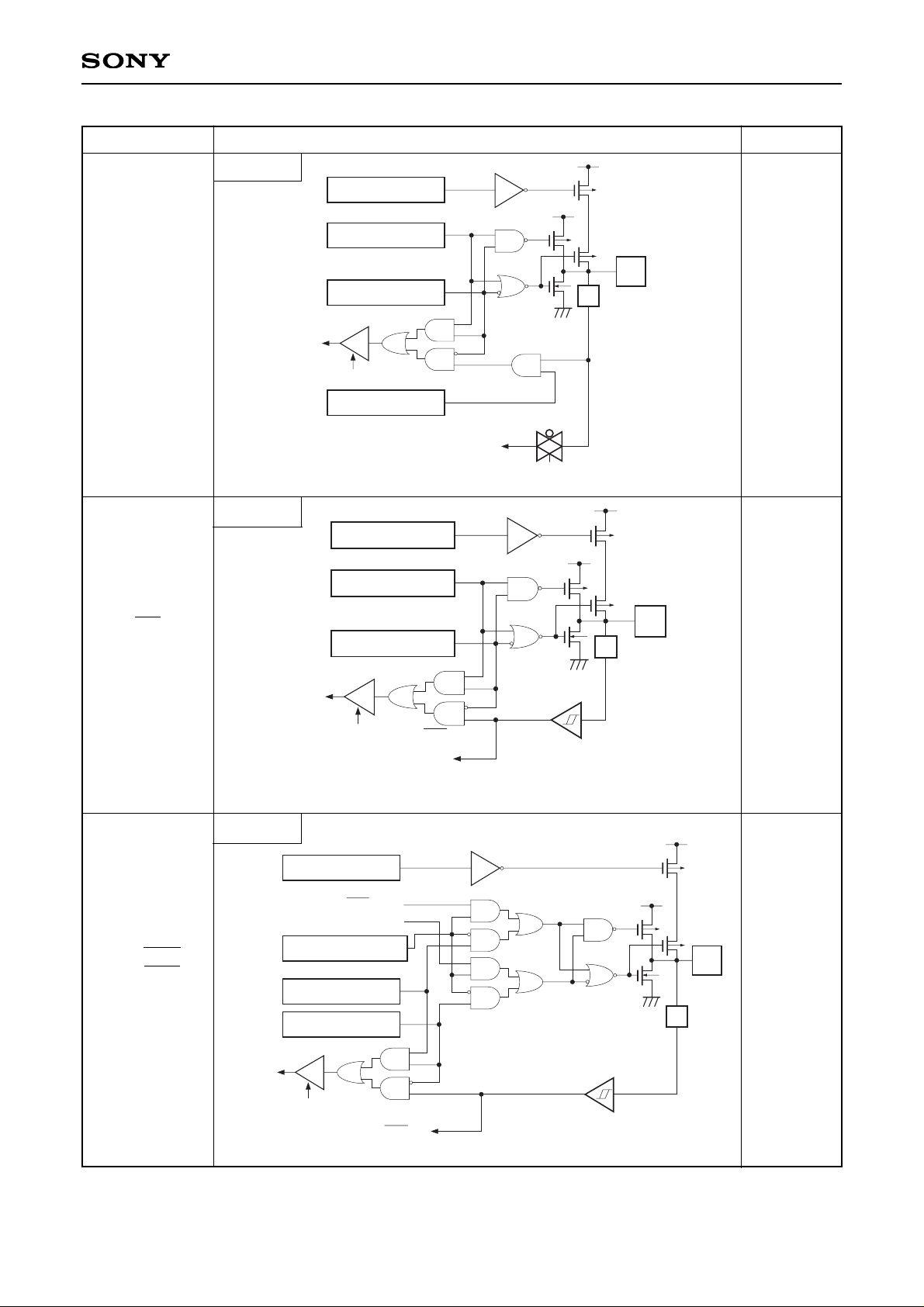
I/O Circuit Format for Pins
Port A
Pin
Circuit format
Pull-up resistor
"0" after a reset
Port B data
∗
Internal data bus
Serial clock output enable
Internal
data bus
Port B direction
"0" after a reset
RD (Port B)
Pull-up resistor
"0" after a reset
SCK OUT
Port B output selection
"0" after a reset
Port B data
Port B direction
"0" after a reset
RD (Port B)
SCK IN
CS0
SI0
SI1
RxD
IP
Schmitt input
∗
Pull-up transistor approx. 100kΩ
∗
Pull-up transistor approx. 100kΩ
(PB0/TxD excluded)
IP
Schmitt input
∗

– 7 –
CXP82032/82040/82052/82060
2 pins
Hi-Z
Hi-Z
Pin
After a reset
Circuit format
PB4/SO0
PB7/SO1
PC0/KR0
to
PC7/KR7
8 pins
6 pins
Hi-Z
PE0/EC0/INT0
PE1/EC1/INT1
PE2/INT2
PE3/INT3/NMI
PE4/RMC
PE5/CINT
IP
Schmitt input
Internal data bus
EC0/INT0
EC1/INT1
INT2
INT3/NM1
RMC
CINT
RD (PortE)
IP
Pull-up resistor
Port C data
Port C direction
"0" after a reset
RD (Port C)
Internal data bus
∗
1
Large current 12mA
∗
2
Pull-up transistor approx. 100kΩ
∗
2
"0" after a reset
∗
1
Key input signak
∗
Pull-up transistor approx. 100kΩ
Pull-up resistor
Port B data
Port B direction
"0" after a reset
RD (Port B)
Internal
data bus
IP
∗
"0" after a reset
Serial data output enable
Port B output selection
"0" after a reset
SO
Port E
Port C
Port B
1 pin
PE6/PWM
Port E output selection
Port E data
RD (Port E)
Internal data bus
"1" after a reset
"0" after a reset
PWM
Output enable
Port E
High level
 Loading...