

Sony CXL5508P, CXL5508M Datasheet
CMOS-CCD 1H Delay Line for PAL
Description
The CXL5508M/P are CMOS-CCD delay line ICs
that provide 1H delay time for PAL signals, including
the external low-pass filter.
Features
• Single 5V power supply
• Low power consumption 60mW (Typ.)
• Built-in peripheral circuits
Functions
• 565-bit CCD register
• Clock driver
• Auto-bias circuit
• Input clamp circuit
• Sample-and-hold circuit
Structure
CMOS-CCD
Absolute Maximum Ratings (Ta = 25°C)
• Supply voltage VDD 6V
•Operating temperature Topr –10 to +60 °C
• Storage temperature Tstg –55 to +150 °C
• Allowable power dissipation
PD
CXL5508M 350 mW
CXL5508P 480 mW
Recommended Operating Condition (Ta = 25°C)
Supply voltage VDD 5 ± 5% V
Recommended Clock Conditions (Ta = 25°C)
• Input clock amplitude VCLK 0.3 to 1.0 Vp-p
(0.5Vp-p typ.)
• Clock frequency fCLK 8.867238 MHz
• Input clock waveform Sine wave
Input Signal Amplitude
VSIG 500mVp-p (Typ.), 527mVp-p (Max.)
(at internal clamp condition)
– 1 –
E91101A7X-PS
Sony reserves the right to change products and specifications without prior notice. This information does not convey any license by
any implication or otherwise under any patents or other right. Application circuits shown, if any, are typical examples illustrating the
operation of the devices. Sony cannot assume responsibility for any problems arising out of the use of these circuits.
CXL5508M/P
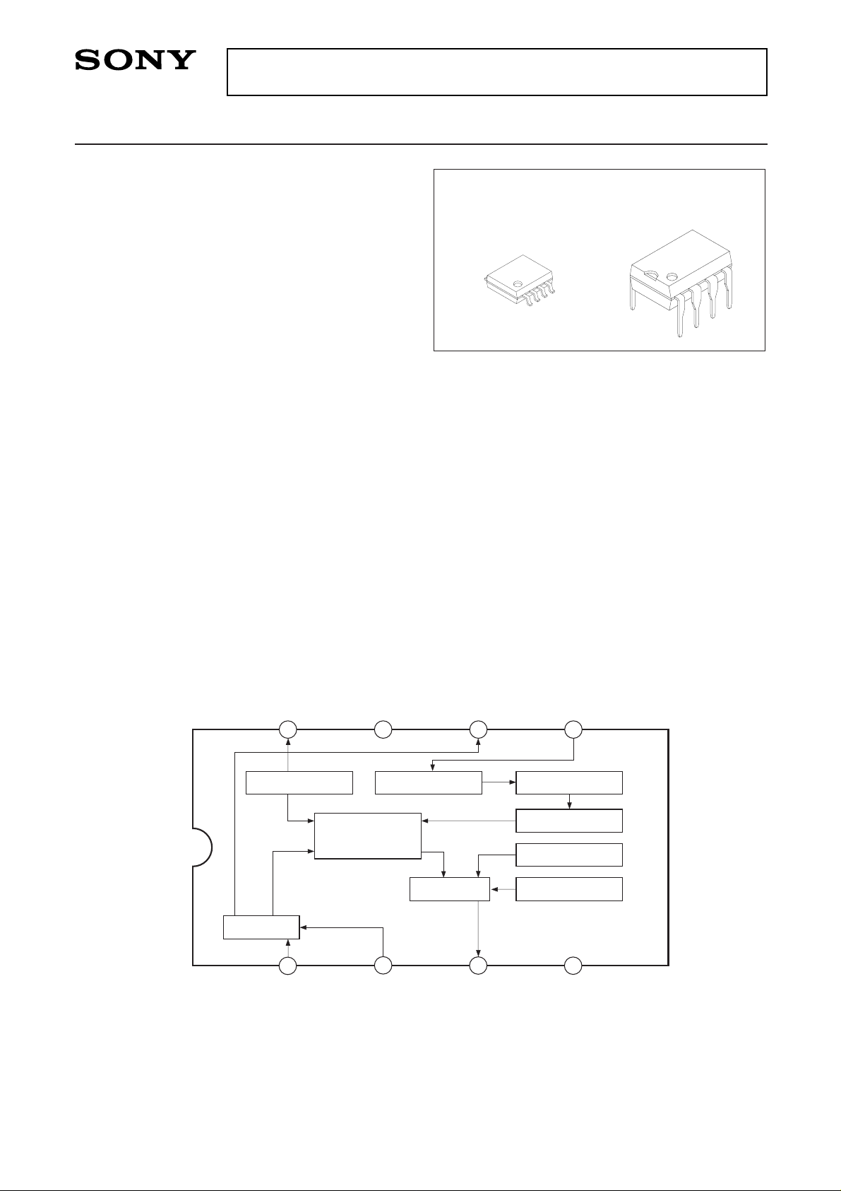
Blook Diagram and Pin Configuration (Top View)
(S/H 1bit)
CLK
1
2
3
4
5
7
8
CCD
(565bit)
6
VGA
V
DD
AB
V
SS
OUT
VGB
IN
Output circuit
Auto-bias circuit
Timing circuit
Bias circuit
Clock driver
Bias circuit (A)
Bias circuit (B)
Clamp circuit
CXL5508M
8 pin SOP (Plastic)
CXL5508P
8 pin DIP (Plastic)

Electrical Characteristics
(Ta = 25°C, VDD = 5V, fCLK = 8.867238MHz, VCLK = 500mVp-p, sine wave)
See "Electrical Characteristics Test Circuit"
– 2 –
CXL5508M/P
Description of I/O Signals
Input signals are low level clamped and output signals are
inverted in relation to the input signals. Also, the clamp
condition of input signals are controlled by VGB (Pin 2)
conditions.
0V ........ Internal clamp condition
5V ........ Non internal clamp condition
Center biased to approx. 2.1V by means of
the IC internal resistance (approx. 10kΩ).
In this mode, the input signal is limited to
APL 50% and the maximum input signal
amplitude is 200mVp-p.
Clamp
level
Input waveform Output waveform
Pin Description
Pin No. Symbol Description Impedance
1
2
3
4
5
6
7
8
IN
VGB
OUT
VSS
CLK
VGA
VDD
AB
Signal input
Gate control B
Signal output
GND
Clock input
Gate control A
Power supply (5V)
Auto-bias DC output
> 10kΩ at no clamp
40 to 500Ω
> 100kΩ
600 to 200kΩ
I
I
O
—
I
O
—
O
I/O
a
a
b
c
—
—
b
b
b
7
–2
–1.8
—
54
37
18
56
12
0
–1.8
—
56
40
20
60
17
2
0
350
—
43
22
64
mA
dB
dB
mVp-p
dB
%
1
2
3
4
5
6
Unit
Note
Max.Min. Typ.
Item Symbol Test condition
SW condition
1
a
a
a
b
b
a
a
a
2
b
b
a
a
a
b
b
b
a
a
b
b
b
a
a
a
—
b
b
a
c
a
a
a
3 4 5
—
200kHz,
500mVp-p, sine wave
200kHz ←→ 2MHz,
150mVp-p, sine wave
No signal input
No signal input
5-staircase wave
(For luminance
signals only)
IDD
GL
fg
CP
SN
LIS
LIL
LIC
Supply current
Low frequency
gain
Frequency
response
S/H pulse
coupling
S/N ratio
Linearity
2.1
2.1
—
Bias
condition
V1 (V)
– 3 –
CXL5508M/P
Notes
(1) This is the IC supply current value during clock and signal input.
(2) GL is the output gain of OUT pin when a 500mVp-p, 200kHz sine wave is fed to IN pin.
GL = 20 log [dB]
(3) Indicates the dissipation at 2MHz in relation to 200kHz.
From the output voltage at OUT pin when a 150mVp-p, 200kHz sine wave is fed to IN pin, and from the
output voltage at OUT pin when a 150mVp-p, 2MHz sine wave is fed to same, cal culation is made
according to the following formula. Input bias is tested at 2.1V.
fg = 20 log [dB]
(4) The internal clock component to the output signal during no-signal input and the leakage of that high
harmonic component are tested. Input bias is tested at 2.1V.
OUT pin output voltage [mVp-p]
500 [mVp-p]
OUT pin otuput voltage (2MHz) [mVp-p]
OUT pin output voltage (200kHz) [mVp-p]
Test value
(mVp-p)
(5) Input no signal noise components are tested with the video noise meter at BPF 10kHz to 3MHz. This is
calculated from the output gain (GL), at the input of 200kHz, 500mVp-p and according to the following
formula.
S/N = –20 • Iog [dB]
(6) Respective outputs are tested at the input of the 5-staircase waves seen in the figure below (Iuminance
signals only) and calculated according to the formula below.
(However, output signals become inverted with regards to input.)
Noise (mVrms)
0.5 • 10
GL/20
40 IRE
100 IRE
500mV
Vs
Vp
Vc
Va
LIS = × 100 [%]
Vs
Va
LIL = × 100 [%]
Vp
Va
LIC = × 100 [%]
Vc
Va
 Loading...