

Sony CXG1017N Datasheet
– 1 –
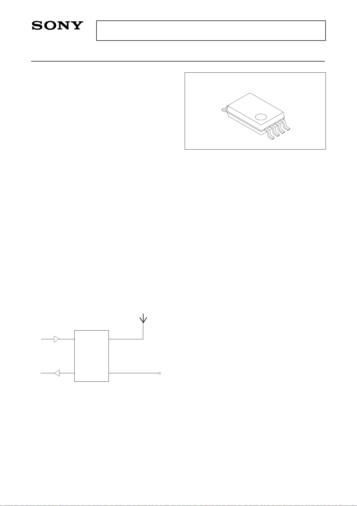
CXG1017N
8 pin SSOP (Plastic)
E97756A79
GSM1800/1900 DPDT TX/RX Antenna Switch
Description
The CXG1017N is a high power DPDT switch
suitable for Digital Cellular applications. This device
is part of a growing family of MMIC Antenna switches
for digital cellular and cordless radios. It uses the
state-of-the-art Sony JFET process.
Features
• Positive voltage supply only
• Low insertion loss, typically 0.7dB at 33dBm input
level
• Stable Characteristics over wide temperature range
• Fast switching-100ns Typical
• Low current consumption, 400µA typical at 5.5V
• 8 pin SSOP package (3.0 × 6.4mm)
Applications
• GSM1800 handportable
• GSM1900 handportable
• DECT basestation/handportable diversity antenna
switching
• Other digital cellular and wireless local loop
applications
Typical Application
ESD
As with other GaAs semiconductors, ESD precautions
must be adhered to.
Sony reserves the right to change products and specifications without prior notice. This information does not convey any license by
any implication or otherwise under any patents or other right. Application circuits shown, if any, are typical examples illustrating the
operation of the devices. Sony cannot assume responsibility for any problems arising out of the use of these circuits.
TX IN
RX OUT
CXG1017N
PA
LNA
Internal
Antenna
External
Antenna
<For Europe and America>
For the availability of this product, please contact the sales office.
– 2 –
CXG1017N
<For Europe and America>
Electrical Characteristics
Measurement Conditions, unless otherwise stated: Vctl (L) = 0V, Vctl (H) = 5.5V,
Pin = 33dBm GSM Burst (577µs pulse length with 8:1 Duty cycle), F = 1.75GHz. Temperature Range –25 to +75°C.
Parameter
Insertion loss
Isolation
VSWR
Switching time
Harmonic levels
Control currents
P0.1dB
P0.3dB
P0.1dB for Vctl (H) = 4.5V
P0.1dB for Vctl (H) = 3.0V
14
0.7
16
100
–56
400
34.5
35.5
34
29
0.95
1.5
–50
800
dB
dB
ns
dBc
µA
dBm
dBm
dBm
dBm
Min. Typ. Max. Unit
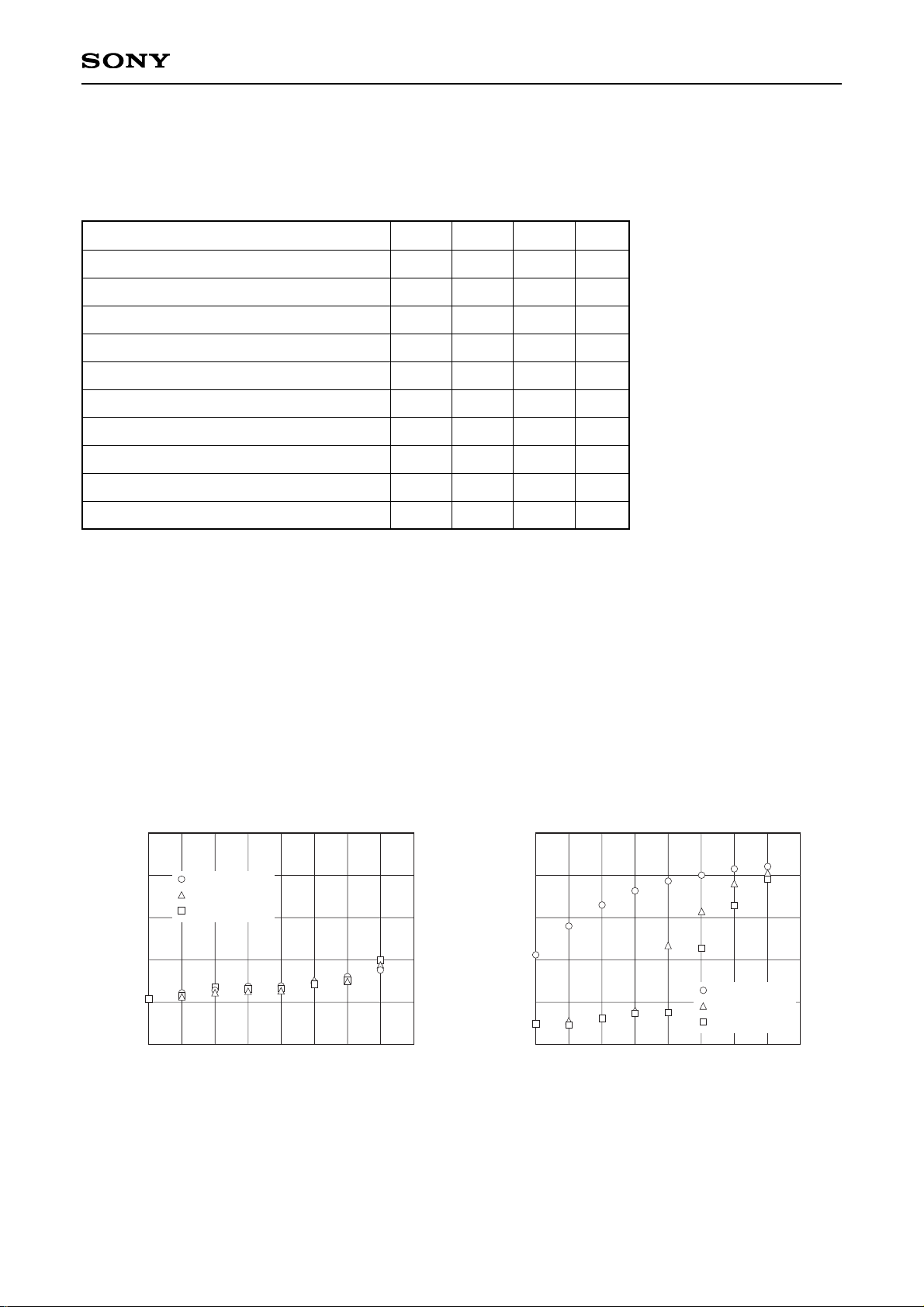
Control Voltage Selection, Vctl (H)
The choice of control voltage will determine the compression characteristic of the switch and the generation of
harmonics. The table above indicates the sensitivity of P0.1dB to control voltage, whilst the graphs below
indicate the sensitivity of harmonic levels:
Vctl = 0/3V
Vctl = 0/4.5V
Vctl = 0/5.5V
–20
–30
–40
–50
–60
–70
30 31 32 33 34 35 36 37 38
Input power [dBm]
2nd Harmonic with Power/Control Volts
Harmonic level [dBc]
Vctl = 0/3V
Vctl = 0/4.5V
Vctl = 0/5.5V
–20
–30
–40
–50
–60
–70
30 31 32 33 34 35 36 37 38
Input power [dBm]
3nd Harmonic with Power/Control Volts
Harmonic level [dBc]
– 3 –
CXG1017N
<For Europe and America>
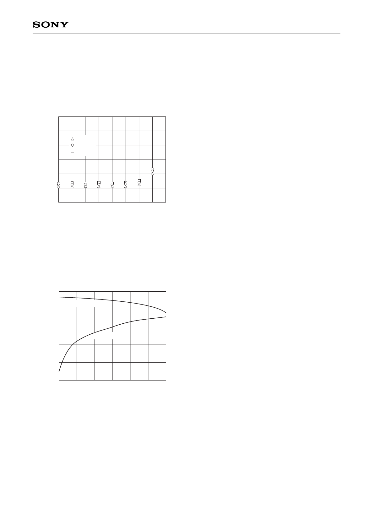
Compression Characteristics
Measurement Conditions: Vctl (L) = 0V, Vctl (H) = 5.5V, GSM Burst, F = 1.75GHz
Temperature range –25 to +75°C.
Typical Characteristics over Temperature:
–25°C
25°C
75°C
1.0
0.5
0
30 31 32 33 34 35 36 37 38
Input power [dBm]
Insertion loss [dB]
1.5
2.0
2.5
3.0
Frequency Characteristics
Measurement Conditions: Vctl (L) = 0V, Vctl (H) = 5.5V, Pin = 0dBm CW, T = 25°C
0
–1
–2
–3
–4
–5
0 1 2 3
Frequency [GHz]
Insertion Loss and Isolation vs. Frequency
Insertion loss [dB]
0
–10
–20
–30
–40
–50
Isolation [dB]
Insertion loss
Isolation
 Loading...