

Sony CXG1008N Datasheet
—1—
E95443B89-TE
Sony reserves the right to change products and specifications without prior notice. This information does not convey any license by
any implication or otherwise under any patents or other right. Application circuits shown, if any, are typical examples illustrating the
operation of the devices. Sony cannot assume responsibility for any problems arising out of the use of these circuits.
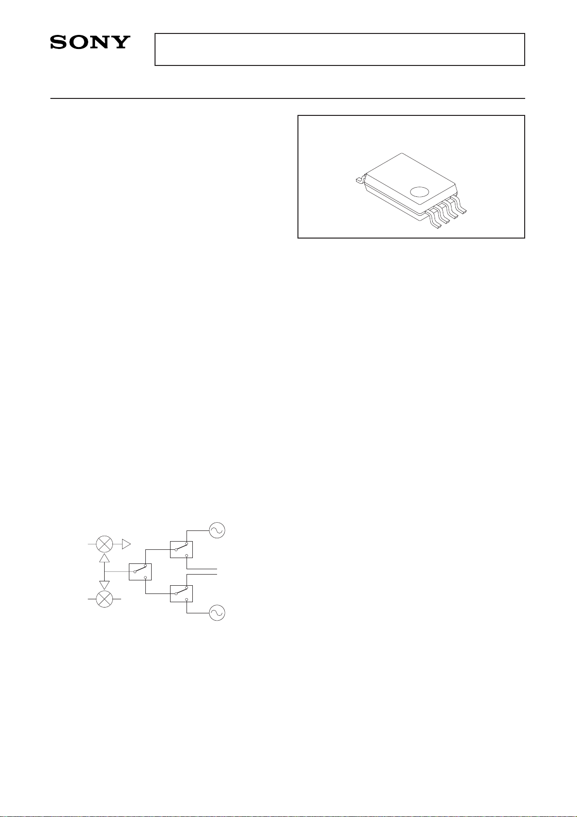
High Isolation SPDT Switch
8 pin SSOP (Plastic)
CXG1008N
ESD
As with other GaAs semiconductors, ESD
precautions must be adhered to.
Description
The CXG1008N is a high isolation SPDT switch
suitable for Digital Cellular applications, Cable TV
and so on. This device is part of a growing family of
MMIC Antenna switches for digital cellular and
cordless radios. It uses the state-of-the-art Sony
GaAs JFET process.
Features
• Positive voltage supply only
• Ultra high isolation, typically 58 dB (GSM 900)
• Low insertion loss, typically 0.7 dB at 20 dBm
input level (GSM 900)
• Stable Characteristics over wide temperature
range
• Fast switching-50 ns Typical
• Low current consumption, 50 µA typical at 3.0 V
• 8 pin SSOP package (3.0 × 6.4 mm)
Applications
• Basestation LO switching
(GSM900/1800/1900, PHS)
• Other Low Power SPDT applications requiring high
isolation (e.g. Cable TV)
Typical Basestation Application
Rx Mixer
Vco1
50ohm
50ohm
Vco2
Tx Mixer
For the availability of this product, please contact the sales office.
—2—
CXG1008N
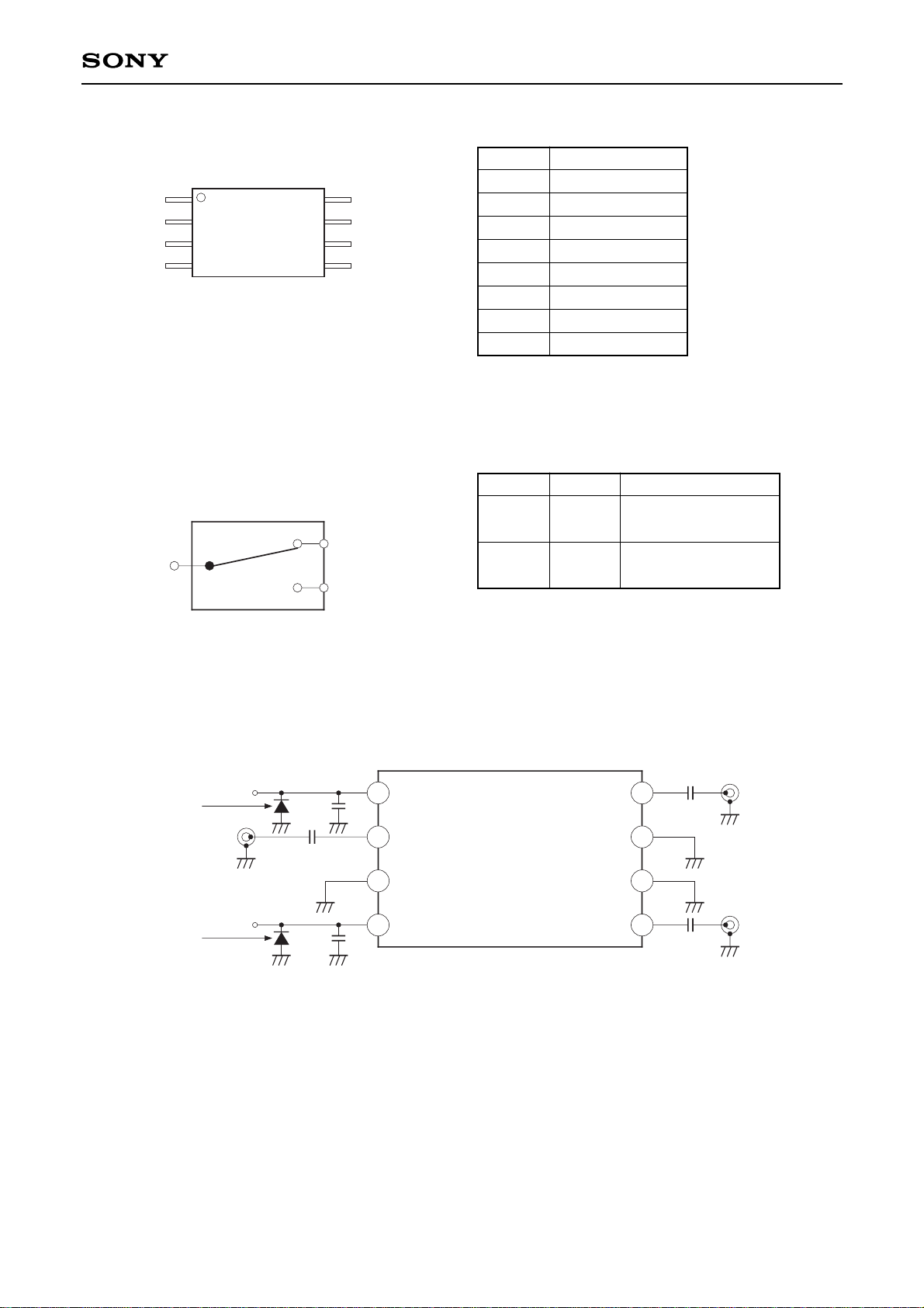
Schematic/Pinout
CTLB
Port1
GND
CTLA
1 8
Port3
GND
GND
Port2
8-pin SSOP (plastic)
Pin No.
1
2
3
4
5
6
7
8
FUNCTION
CONTROL B
RF PORT 1
GROUND
CONTROL A
RF PORT 2
GROUND
GROUND
RF PORT 3
Block Diagram/Truth Table
Block Diagram
External Circuitry
Port1
Port3
Port2
VCTLA
High
Low
VCTLB
Low
High
Port1-Port2 ON
Port1-Port3 OFF
Port1-Port2 OFF
Port1-Port3 ON
C1
100pF
100pF
C2
Port1
C1
100pF
CTLB
CTLA
D1
D1
CXG1008N
1
2
3
4
Optional
Optional
100pF
C2
Port3
100pF
C2
Port2
8
7
6
5
When using the CXG1008N, the following external components should be used:
C1: This is used for signal line filtering. 100 pF is recommended.
C2: This is used for RF De-coupling and must be used in all applications. 100 pF is recommended.
D1: 6.2 V Zener diodes may be incorporated at the Control lines, as indicated, in order to give improved
ESD performance if necessary.
<For GSM Application>
—3—
CXG1008N
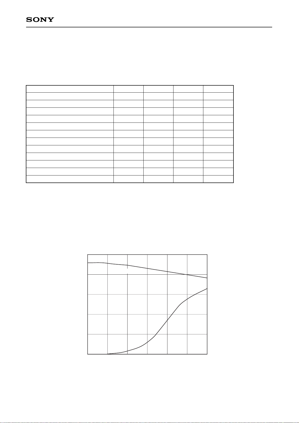
Application GSM900/1800/1900 Basestation LO switching
Electrical Characteristics
Measurement Conditions, Vctl (L)=0 V, Vctl (H)=5 V,
Ta=25 °C
Parameter
Insertion loss @ 900 MHz
Isolation @ 900 MHz
Insertion loss @ 1500 MHz
Isolation @ 1500 MHz
Insertion loss @ 1900 MHz
Isolation @ 1900 MHz
VSWR ≤ 2 GHz
Switching Time
Control Current (3 V)
P1 dB (Vctl=3 V)
P1 dB (Vctl=4 V)
P1 dB (Vctl=5 V)
Min.
(51) 52
(46) 47
(41) 42
Typ.
0.7
58
0.75
52
0.8
47
1.3
50
50
24
26
28
Max.
∗1.1 (1.2)
1.15 (1.25)
∗1.2 (1.3)
1.5
100
Unit
dB
dB
dB
dB
dB
dB
ns
µA
dBm
dBm
dBm
Frequency Characteristics
Measurement Conditions: Vctl (L)=0 V, Vctl (H)=5 V, Pin=0 dBm CW, T=25 °C
Example of Representative Characteristics (Ta=25 °C)
Insertion loss, isolation vs. Frequency
0
–1
–2
–3
–4
–5
–10
–20
–30
–40
–50
–60
Frequency (GHz)
Insertion loss (dB)
Isolation (dB)
Insertion Loss
Isolation
1 2
∗( ) Temperature Range –35 to +85 °C
 Loading...