

Sony CXD3508ATQ Datasheet

Description
The CXD3508ATQ is a LCD interface IC for the
color LCD module ACX704AKM driver.
Features
• Generates the color LCD module ACX704AKM drive
pulse.
• Standby mode function
• Thin package (100-pin TQFP)
Applications
PDA, compact LCD monitor, etc.
Structure
Silicon gate CMOS IC
Absolute Maximum Ratings (Ta = 25°C)
• Supply voltage VDD Vss – 0.3 to +5.5 V
• Input voltage VI Vss – 0.3 to VDD + 0.3 V
• Output voltage VO Vss – 0.3 to VDD + 0.3 V
• Operating temperature Topr –25 to +75 °C
• Storage temperature Tstg –55 to +125 °C
Recommended Operating Conditions
• Supply voltage VDD 3.0 to 3.6 V
• Operating temperature Topr –10 to +60 °C
LCD Interface IC
– 1 –
E00947
Sony reserves the right to change products and specifications without prior notice. This information does not convey any license by
any implication or otherwise under any patents or other right. Application circuits shown, if any, are typical examples illustrating the
operation of the devices. Sony cannot assume responsibility for any problems arising out of the use of these circuits.
CXD3508ATQ
100 pin TQFP (Plastic)
For the availability of this product, please contact the sales office.
– 2 –
CXD3508ATQ
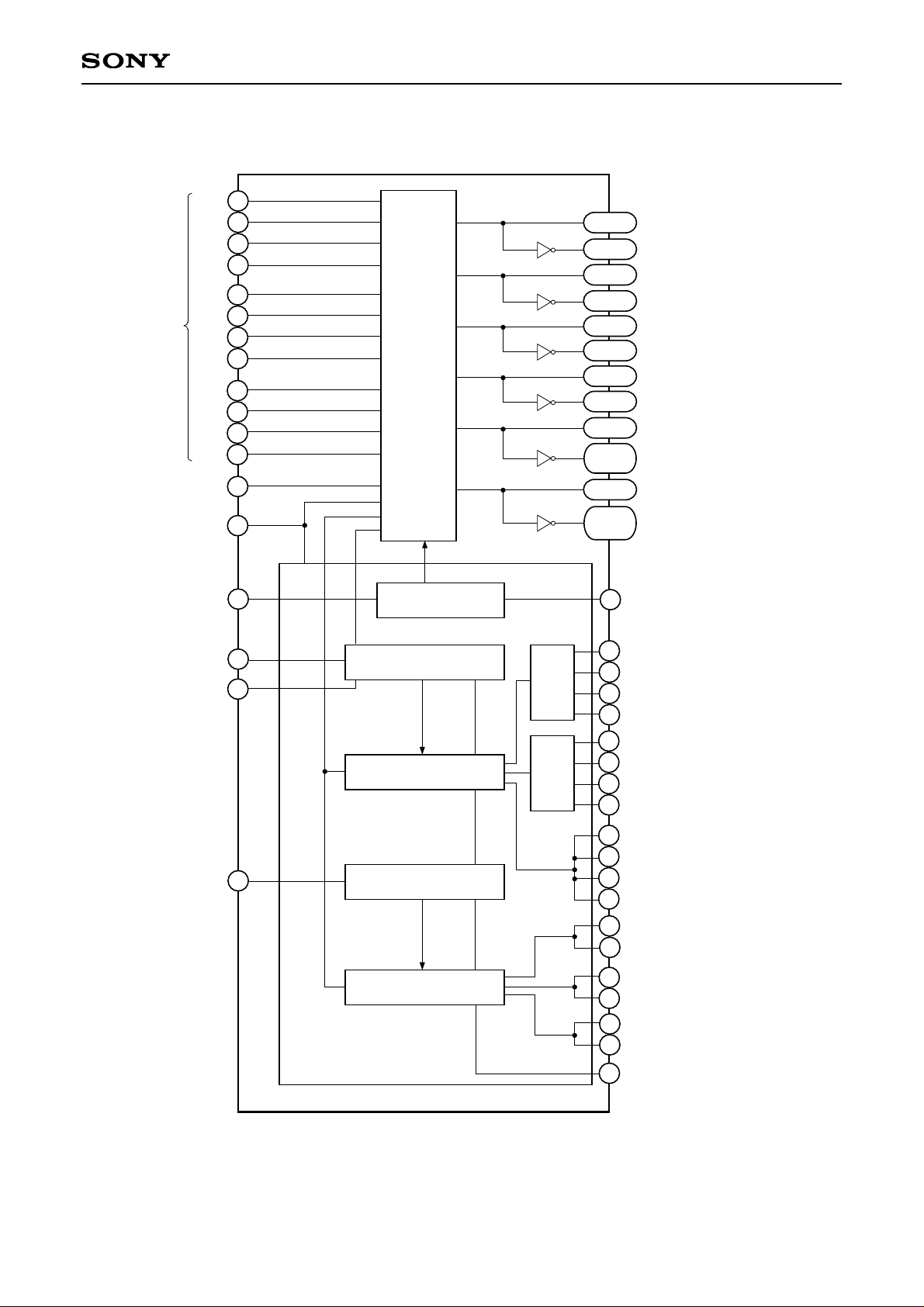
Block Diagram
6
7
8
9
10
11
12
13
14
15
16
17
R0
R1
R2
R3
G0
G1
DATA IN
G2
G3
B0
B1
B2
B3
FA
MCK
PCI
Hsync/DENB
SLIN
V sync
24
20
21
18
19
31 to 28
R01, R11, R21, R31
43 to 41
XR01, XR11, XR21, XR31
94 to 97
R02, R12, R22, R32
82 to 89
XR02, XR12, XR22, XR32
35 to 32
G01, G11, G21, G31
47 to 44
XG01, XG11, XG21, XG31
90 to 93
G02, G12, G22, G32
78 to 81
XG02, XG12, XG22, XG32
39 to 36
B01, B11, B21, B31
53, 52,
49, 48
XB01, XB11, XB21, XB31
72 to 74,
77
B02, B12, B22, B32
86 to 89
XB02, XB12, XB22, XB32
PCO
HST1
XHST1
HST2
XHST2
HCK1
XHCK1
HCK2
XHCK2
OE1
XOE1
OE2
XOE2
VST
XVST
VCK
XVCK
ENB
XENB
FRP
27
64
65
66
67
54
55
56
57
58
59
Delay
DelayH Timing Pulse GEN.
H Counter
Power CTR.
V Counter
V Timing Pulse GEN.
60
61
62
63
68
69
70
71
98
Timing Generator Block
Serial/
Parallel
Conversion
Block
22
– 3 –
CXD3508ATQ
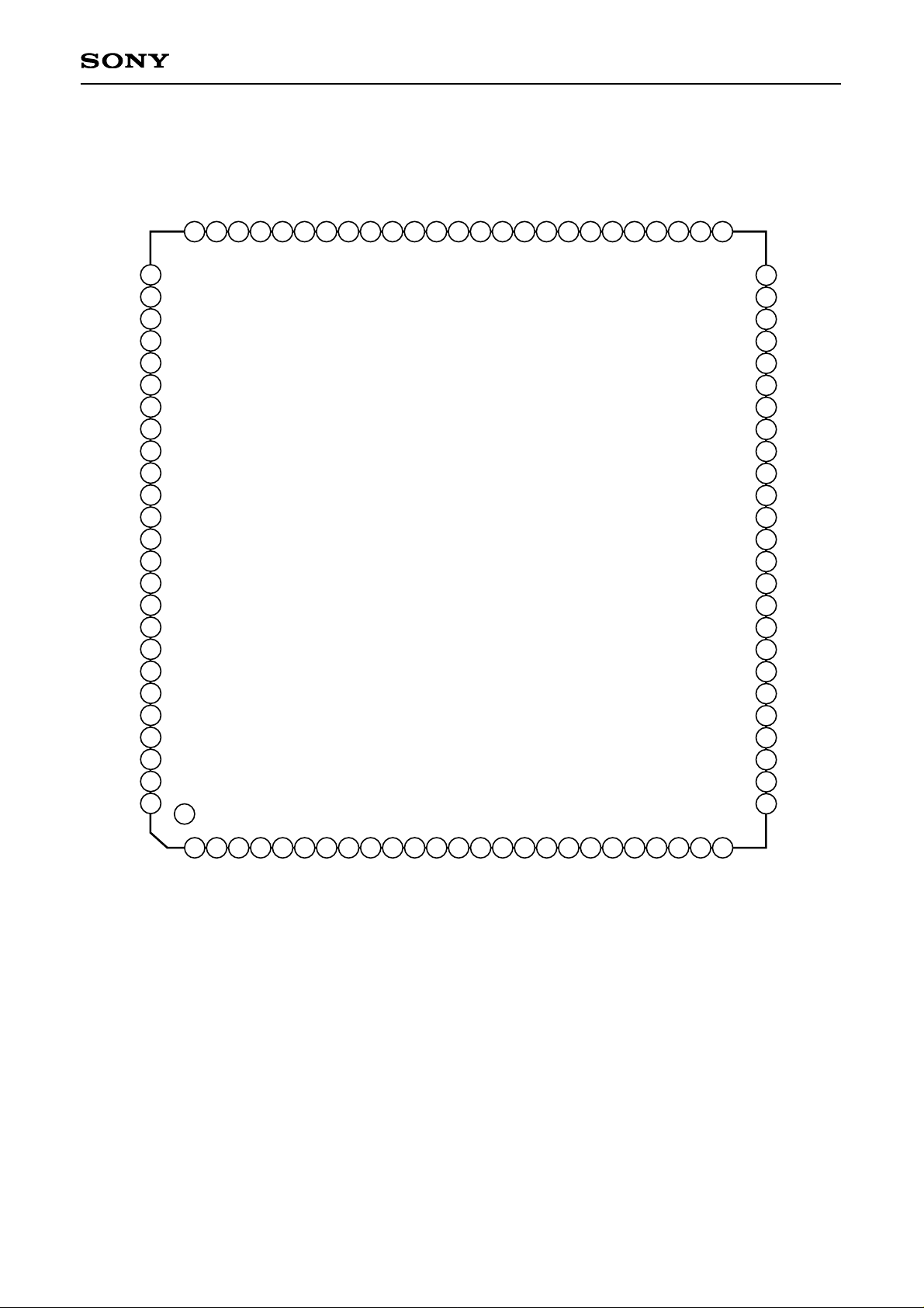
Pin Configuration
1 2 3 4 5 6 7 8 9 101112 13 14 15
16
17
18 19 202122 23 24 25
26
27
28
29
30
31
32
33
34
35
36
37
38
39
40
41
42
43
44
45
46
47
48
49
50
51525354555657585960616263646566676869707172737475
76
77
78
79
80
81
82
83
84
85
86
87
88
89
90
91
92
93
94
95
96
97
98
99
100
VSS
TEST1
TEST2
V
SS
CLR
R3R2R1
R0
G3G2G1
G0
B3B2B1
B0
Hsync/DENB
Vsync
MCK
PCI
SLIN
TESTP
FA
V
SS
VDD
XB21
XB31
XG01
XG11
XG21
XG31
XR01
XR11
XR21
XR31
B01
B11
B21
B31
G01
G11
G21
G31
R01
R11
R21
R31
PCO
V
DD
VDD
XB32
XG02
XG12
XG22
XG32
XR02
XR12
XR22
XR32
B02
B12
B22
B32
G02
G12
G22
G32
R02
R12
R22
R32
FRP
TESTV
V
DD
VSS
XB22
XB12
XB02
XOE2
OE2
XOE1
OE1
XHST2
HST2
XHST1
HST1
XHCK2
HCK2
XHCK1
HCK1
XVCK
VCK
XENB
ENB
XVST
VST
XB01
XB11
V
SS

– 4 –
CXD3508ATQ
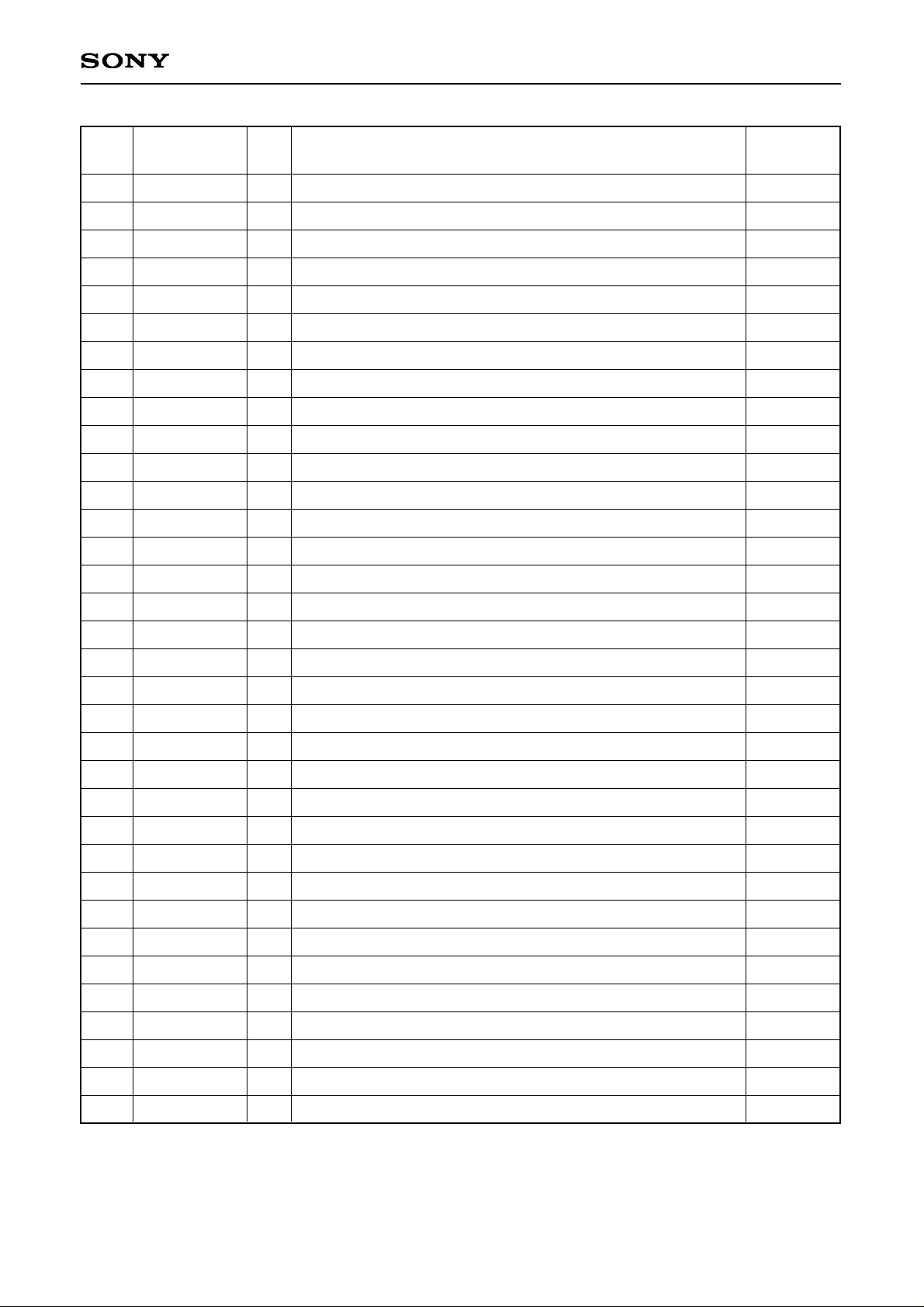
Pin Description
Pin
No.
1
2
3
4
5
6
7
8
9
10
11
12
13
14
15
16
17
18
19
20
21
22
23
24
25
26
27
28
29
30
31
32
33
VSS
TEST1
TEST2
VSS
CLR
R3
R2
R1
R0
G3
G2
G1
G0
B3
B2
B1
B0
Hsync/DENB
Vsync
MCK
PCI
SLIN
TESTP
FA
VSS
VDD
PCO
R31
R21
R11
R01
G31
G21
—
I
I
—
I
I
I
I
I
I
I
I
I
I
I
I
I
I
I
I
I
I
I
I
—
—
O
O
O
O
O
O
O
GND
Test signal input (Connect to GND)
Test signal input (Connect to GND)
GND
System reset
Red signal input (MSB)
Red signal input
Red signal input
Red signal input (LSB)
Green signal input (MSB)
Green signal input
Green signal input
Green signal input (LSB)
Blue signal input (MSB)
Blue signal input
Blue signal input
Blue signal input (LSB)
Hsync/data enable pulse input
Vsync pulse input
Dot clock input
Power control signal input
Sync input signal mode switch
Test signal input (Connect to VDD)
Data phase adjustment (Connect to GND)
GND
Power supply
Power control signal output
Red signal output
Red signal output
Red signal output
Red signal output
Green signal output
Green signal output
—
DWN
∗1
DWN
∗1
—
UP
∗2
—
—
—
—
—
—
—
—
—
—
—
—
—
—
—
—
DWN
∗1
DWN
∗1
DWN
∗1
—
—
—
—
—
—
—
—
—
Symbol I/O Description
Input pin for
open status
∗1
Built-in pull-down resistor (50kΩ typ.)
∗2
Built-in pull-up resistor (50kΩ typ.)
– 5 –
CXD3508ATQ
34
35
36
37
38
39
40
41
42
43
44
45
46
47
48
49
50
51
52
53
54
55
56
57
58
59
60
61
62
63
64
65
66
67
G11
G01
B31
B21
B11
B01
XR31
XR21
XR11
XR01
XG31
XG21
XG11
XG01
XB31
XB21
VDD
VSS
XB11
XB01
VST
XVST
ENB
XENB
VCK
XVCK
HCK1
XHCK1
HCK2
XHCK2
HST1
XHST1
HST2
XHST2
O
O
O
O
O
O
O
O
O
O
O
O
O
O
O
O
—
—
O
O
O
O
O
O
O
O
O
O
O
O
O
O
O
O
Green signal output
Green signal output
Blue signal output
Blue signal output
Blue signal output
Blue signal output
Red signal output (inverse)
Red signal output (inverse)
Red signal output (inverse)
Red signal output (inverse)
Green signal output (inverse)
Green signal output (inverse)
Green signal output (inverse)
Green signal output (inverse)
Blue signal output (inverse)
Blue signal output (inverse)
Power supply
GND
Blue signal output (inverse)
Blue signal output (inverse)
VST pulse output
VST pulse output (inverse)
ENB pulse output
ENB pulse output (inverse)
VCK pulse output
VCK pulse output (inverse)
HCK1 pulse output
HCK1 pulse output (inverse)
HCK2 pulse output
HCK2 pulse output (inverse)
HST1 pulse output
HST1 pulse output (inverse)
HST2 pulse output
HST2 pulse output (inverse)
—
—
—
—
—
—
—
—
—
—
—
—
—
—
—
—
—
—
—
—
—
—
—
—
—
—
—
—
—
—
—
—
—
—
Pin
No.
Symbol I/O Description
Input pin for
open status
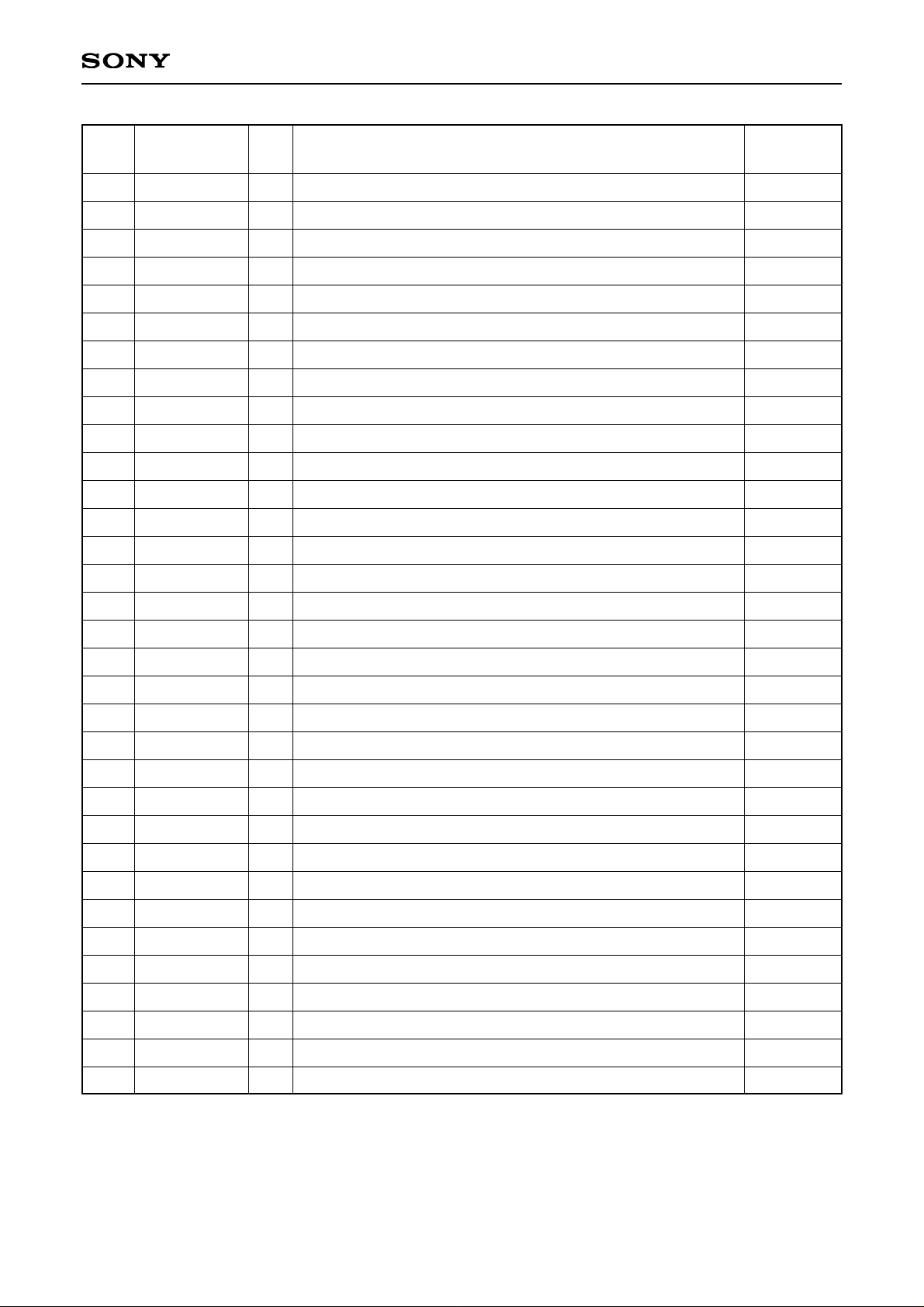
– 6 –
CXD3508ATQ
68
69
70
71
72
73
74
75
76
77
78
79
80
81
82
83
84
85
86
87
88
89
90
91
92
93
94
95
96
97
98
99
100
OE1
XOE1
OE2
XOE2
XB02
XB12
XB22
VSS
VDD
XB32
XG02
XG12
XG22
XG32
XR02
XR12
XR22
XR32
B02
B12
B22
B32
G02
G12
G22
G32
R02
R12
R22
R32
FRP
TESTV
V
DD
O
O
O
O
O
O
O
—
—
O
O
O
O
O
O
O
O
O
O
O
O
O
O
O
O
O
O
O
O
O
O
I
—
OE1 pulse output
OE1 pulse output (inverse)
OE2 pulse output
OE2 pulse output (inverse)
Blue signal output (inverse)
Blue signal output (inverse)
Blue signal output (inverse)
GND
Power supply
Blue signal output (inverse)
Green signal output (inverse)
Green signal output (inverse)
Green signal output (inverse)
Green signal output (inverse)
Red signal output (inverse)
Red signal output (inverse)
Red signal output (inverse)
Red signal output (inverse)
Blue signal output
Blue signal output
Blue signal output
Blue signal output
Green signal output
Green signal output
Green signal output
Green signal output
Red signal output
Red signal output
Red signal output
Red signal output
Polarity inversion pulse signal output
Test signal input (Connect to GND)
Power supply
—
—
—
—
—
—
—
—
—
—
—
—
—
—
—
—
—
—
—
—
—
—
—
—
—
—
—
—
—
—
—
DWN
∗1
—
Pin
No.
Symbol I/O Description
Input pin for
open status
∗
1
Built-in pull-down resistor (50kΩ typ.)
 Loading...