

Sony CXD3503R Datasheet

Color Shading Correction IC for Liquid Crystal Projectors
Description
The CXD3503R is a color shading correction IC for
Sony data projectors. Used together with the Sony
LCD driver CXA2111R or CXA2112R, this IC corrects
color shading caused by the LCD panel structure or
the optical system. This IC has a built-in SRAM and
D/A converter, and 16 horizontal and 13 vertical
correction points can be set via a serial interface.
Functions
• Generates the color shading correction signals for
the high-temperature polysilicon TFT LCD panels
used in Sony projectors
• Supports various SVGA, XGA and SXGA signals
using 1/2 dot clock input
• Vertical output signal interpolation using an internal
arithmetic circuit
• Automatic determination of eliminated lines during
pulse eliminator display when used together with
the Sony timing generator ICs CXD2464R or
CXD3500R
• Supports up/down and/or right/left inversion
• Supports LCD panel display area switching
conversion functions
• Standby and correction OFF functions
Applications
Liquid crystal projectors, etc.
Structure
Silicon gate CMOS IC
Absolute Maximum Ratings (VSS = 0V)
• Supply voltage VDD VSS – 0.3 to +7.0 V
• Input voltage VI VSS – 0.3 to VDD + 0.3 V
• Output voltage VO VSS – 0.3 to VDD + 0.3 V
• Storage temperature
Tstg –55 to +125 °C
• Operating temperature
Topr –40 to +85 °C
Recommended Operating Conditions
(Ta = –20 to +75°C, VSS = 0V)
Supply voltage VDD 4.5 to 5.5 V
– 1 –
E99432-PS
Sony reserves the right to change products and specifications without prior notice. This information does not convey any license by
any implication or otherwise under any patents or other right. Application circuits shown, if any, are typical examples illustrating the
operation of the devices. Sony cannot assume responsibility for any problems arising out of the use of these circuits.
CXD3503R
64 pin LQFP (Plastic)
Note) Company names and product names, etc. contained in these materials are trademarks or registered trademarks of the
respective companies.
– 2 –
CXD3503R
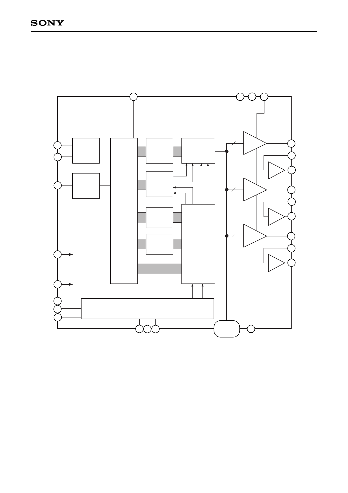
Block Diagram
32 33
44
DAC
DAC
DAC
6bit
36
37
38
41
42
43
46
47
48
Buff.
Buff.
Buff.
40
6bit
6bit
567
Data
31
60
3
4
61
63
57
58
59
DACO2
DACKI
DACKO
HSYNC
VST
HST
CKI
XCLR
SCTR
SCLK
SDAT
RGT
DWN
CTRL
DOUT
VRL
VRH
OLIM
BFIN2
AOUT2
DACO1
BFIN1
AOUT1
DACO0
BFIN0
AOUT0
H, V
detector
Main
controller
Buff.
Memory
controller
Buff.
Memory
(SRAM)
Main
Memory
(SRAM)
Operation
block
V up/down
counter
H up/down
counter
Serial I/F Block
Eliminator
Master clock
System clear
11 to 16,
18 to 23,
25 to 30
– 3 –
CXD3503R
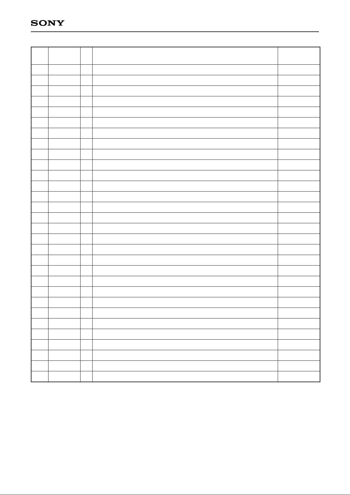
Pin Description
Pin
No.
Symbol I/O Description
Processing for
internal input
1
2
3
4
5
6
7
8
9
10
11
12
13
14
15
16
17
18
19
20
21
22
23
24
25
26
27
28
29
30
31
32
33
34
NC
NC
VST
HST
DWN
RGT
CTRL
TEST0
TEST1
TEST2
DOUT00
DOUT01
DOUT02
DOUT03
DOUT04
DOUT05
DVSS0
DOUT10
DOUT11
DOUT12
DOUT13
DOUT14
DOUT15
DVDD0
DOUT20
DOUT21
DOUT22
DOUT23
DOUT24
DOUT25
DACKO
DACKI
OLIM
DVDD1
—
—
I
I
I
I
I
I
I
I
O
O
O
O
O
O
—
O
O
O
O
O
O
—
O
O
O
O
O
O
O
I
I
—
Not connected
Not connected
VST pulse input
HST pulse input
Up/down inversion control input (H: down scan, L: up scan)
Right/left inversion control input (H: normal scan, L: reverse scan)
Up/down and/or right/left inversion control signal (Serial settings
selected when L.)
Test (Leave open.)
Test (Leave open.)
Test (Leave open.)
Digital data output 00
Digital data output 01
Digital data output 02
Digital data output 03
Digital data output 04
Digital data output 05
Digital GND
Digital data output 10
Digital data output 11
Digital data output 12
Digital data output 13
Digital data output 14
Digital data output 15
Digital VDD (5V)
Digital data output 20
Digital data output 21
Digital data output 22
Digital data output 23
Digital data output 24
Digital data output 25
DAC clock output (Connect to DACKI.)
DAC clock input (Connect to DACKO.)
Digital data output limiter (H: Hi-Z, L: digital data output)
Digital VDD (5V)
—
—
—
—
—
—
—
L
L
L
—
—
—
—
—
—
—
—
—
—
—
—
—
—
—
—
—
—
—
—
—
—
—
—
– 4 –
CXD3503R
35
36
37
38
39
40
41
42
43
44
45
46
47
48
49
50
51
52
53
54
55
56
57
58
59
60
61
62
63
64
DVSS1
DACO2
BFIN2
AOUT2
AVSS
VRL
DACO1
BFIN1
AOUT1
VRH
AVDD
DACO0
BFIN0
AOUT0
DVSS2
NC
NC
NC
NC
NC
NC
DVDD2
SCTR
SCLK
SDAT
HSYNC
XCLR
DVSS3
CKI
SLCK
—
O
I
O
—
I
O
I
O
I
—
O
I
O
—
—
—
—
—
—
—
—
I
I
I
I
I
—
I
I
Digital GND
DAC output 2
Buffer input 2
Correction signal output 2
Analog GND
DAC output low reference voltage input
DAC output 1
Buffer input 1
Correction signal output 1
DAC output high reference voltage input
Analog power supply
DAC output 0
Buffer input 0
Correction signal output 0
Digital GND
Not connected
Not connected
Not connected
Not connected
Not connected
Not connected
Digital VDD (5V)
Serial chip select input (serial transfer block)
Serial clock input (serial transfer block)
Serial data input (serial transfer block)
HSYNC input
Clear (L: system clear)
Digital GND
Master clock input
Clock switching (H: Internal 1/2 frequency divider used.)
—
—
—
—
—
—
—
—
—
—
—
—
—
—
—
—
—
—
—
—
—
—
—
—
—
—
H
—
—
—
Pin
No.
Symbol I/O Description
Processing for
internal input
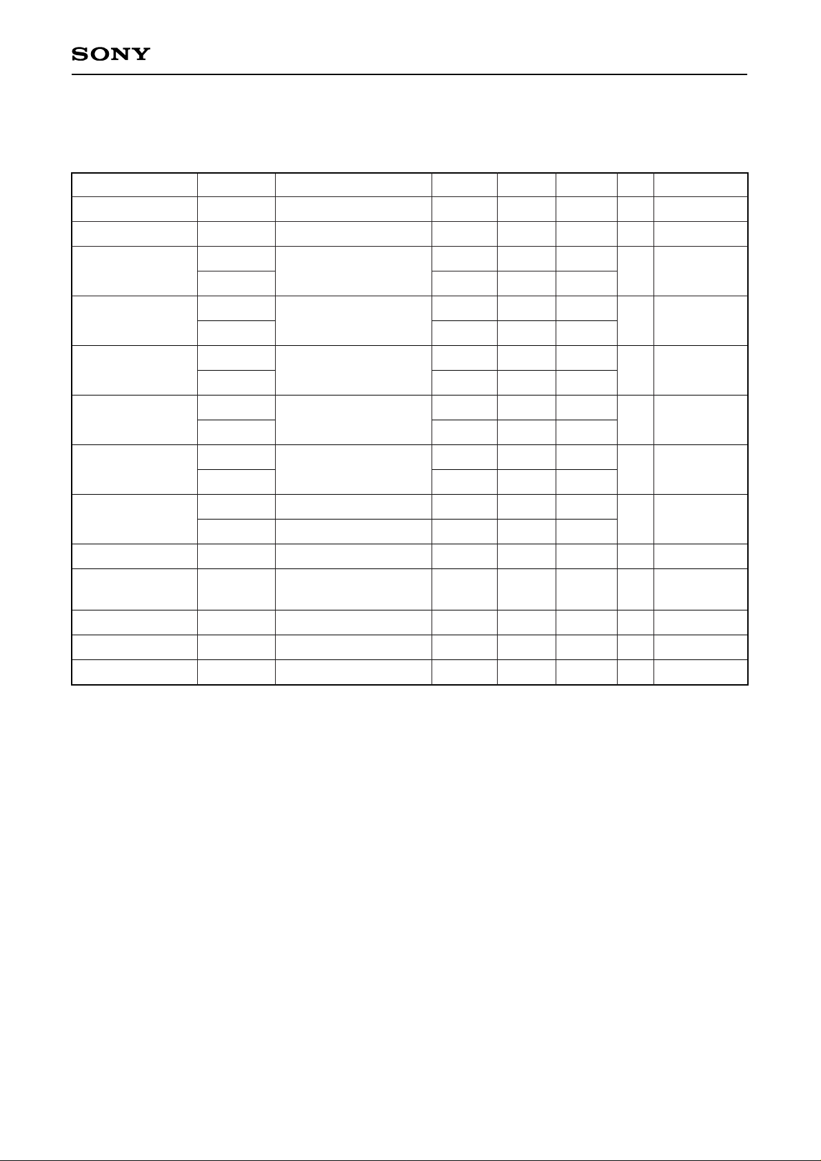
– 5 –
CXD3503R
IOH = –4mA
IOL = 4mA
VI = VDD, VSS
During high impedance
output
During 41MHz operation
Input voltage 2
Input voltage 3
Input voltage 4
Input voltage 5
Output voltage 1
Input leak current
Output leak
current
Pull-up resistor
Pull-down resistor
Current consumption
(INPUT)
∗1
CTRL, DACKI, DWN, HST, OLIM, RGT, SLCK, VST
∗2
TEST0, 1, 2
∗3
HSYNC, SCLK, SCTR, SDAT
∗4
XCLR
∗5
CKI
(OUTPUT)
∗6
DACKO
∗7
DOUT00 to 05, DOUT10 to 15, DOUT20 to 25
Note) AOUT0, 1 and 2, DACO0, 1 and 2, BFIN0, 1 and 2, VRH and VRL are not included in the DC characteristics.
V
V
V
V
µA
µA
kΩ
kΩ
mA
∗2
∗5
∗3
Electrical Characteristics
DC Characteristics
(VDD = 5.0 ± 0.5V, VSS = 0V, Topr = –40 to +85°C)
Item
VDD
VI, VO
VIH
VIL
VIH
VIL
VIH
VIL
VIH
VIL
VIH
VIL
VOH
VOL
IIL
IOZ
RUP
RDN
IDD
4.5
VSS
0.7VDD
0.7VDD
0.7VDD
2.2
2.5
VDD – 2.1
–10
–10
60
45
5.0
120
90
60
5.5
VDD
0.3VDD
0.3VDD
0.3VDD
0.8
0.6
0.4
10
10
240
180
Symbol Conditions Min. Typ. Max. Unit
Supply voltage
Input, output voltage
Input voltage 1
Applicable pins
V
V
V
V
∗1
∗4
CMOS input
CMOS input
With pull-up resistor
CMOS input
With pull-down resistor
TTL input
TTL Schmitt input
∗6, ∗7
∗1, ∗3, ∗5
∗7
∗4
∗2
– 6 –
CXD3503R
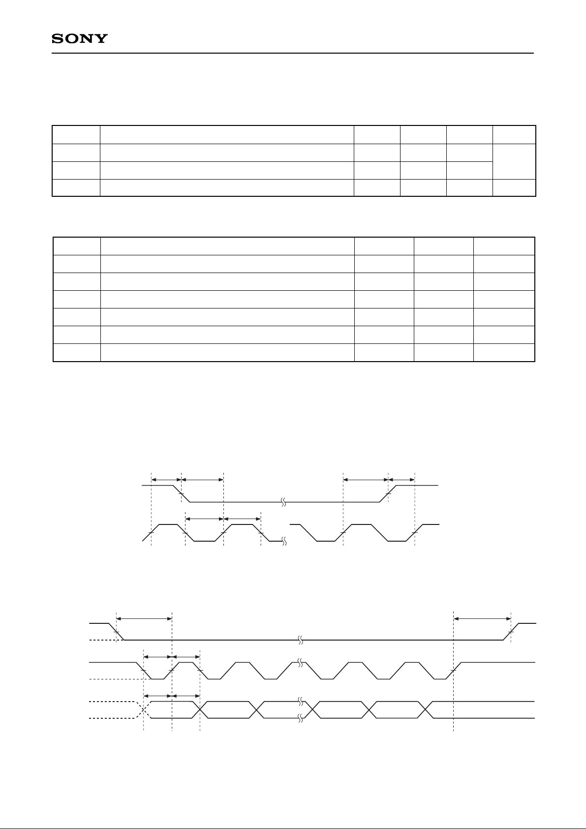
AC Characteristics
External Clock Input AC Characteristics
(VDD = 5.0 ± 0.5V, VSS = 0V, Topr = –40 to +85°C)
Serial Transfer AC Characteristics (VDD = 5.0 ± 0.5V, VSS = 0V, Topr = –40 to +85°C)
Item
SCTR setup time, activated by the rising edge of SCLK
SDAT setup time, activated by the rising edge of SCLK
SCTR hold time, activated by the rising edge of SCLK
SDAT hold time, activated by the rising edge of SCLK
SCLK L level pulse width
SCLK H level pulse width
8Tns
4Tns
8Tns
4Tns
4Tns
4Tns
—
—
—
—
—
—
Min. Typ.
—
—
—
—
—
—
Max.
ts0
ts1
th0
th1
tW1L
tW1H
Symbol
T: Input clock cycle
Item
HSYNC setup time, activated by the rising edge of CKI
HSYNC hold time, activated by the rising edge of CKI
CKI L/H level pulse width
12
0.5
—
—
—
50
Min. Typ.
—
—
—
ns
%
Max. Unit
ts0
th0
tWL/tWH
Symbol
Timing Definition
External Clock Input AC Characteristics
Serial Transfer AC Characteristics
HSYNC
(negative
polarity)
CKI1, 2
50%
th0 ts0
twL twH
50% 50%
50%
th0 ts0
50%
50%
SCTR
SCLK
SDAT
ts0
tw1L tw1H
ts1 th1
50%
50%
50%
th0
 Loading...