


CXD3300R
10-bit 20MSPS Video A/D Converter
Description
The CXD3300R is a 10-bit CMOS A/D converter for
video applications. This IC is ideally suited for the
A/D conversion of video signals in TVs, VCRs,
camcorders, etc.
Features
• Resolution: 10 bits ± 1.0LSB (D.L.E.)
• Maximum sampling frequency: 20MSPS
• Low power consumption: 40mW
(Except self-bias )
• Low input capacitance
• Built-in self-bias circuit
Absolute Maximum Ratings (Ta = 25°C)
• Supply voltage AVDD AVSS – 0.5 to +4.5 V
DVDD DVSS – 0.5 to +4.5 V
• Reference voltage VRT, VRB AVDD + 0.5 to AVSS – 0.5 V
• Input voltage VIN AVDD + 0.5 to AVSS – 0.5 V
(analog)
• Input voltage VIH, VIL AVDD + 0.5 to AVSS – 0.5 V
(digital)
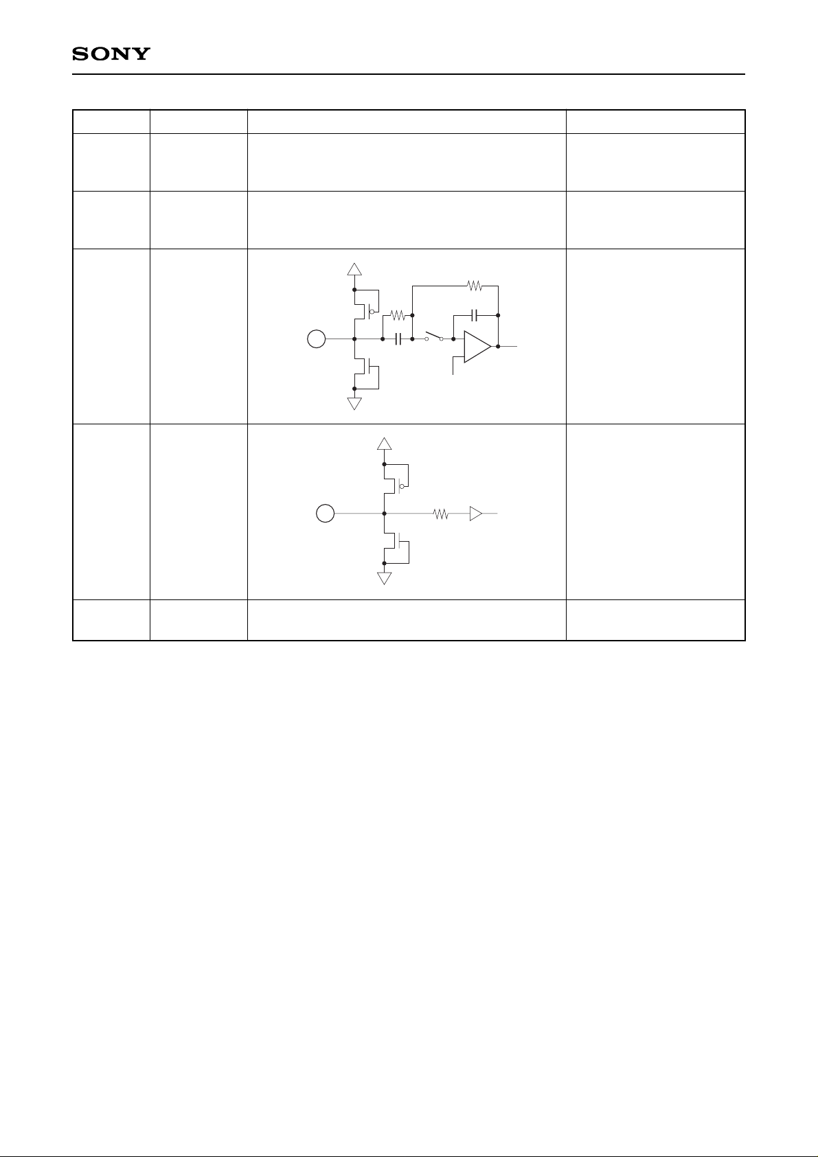
• Output voltage VOH, VOL DVDD + 0.5 to DVSS – 0.5 V
(digital)
• Storage temperature Tstg –55 to +150 °C
Recommended Operating Conditions
• Supply voltage AVDD, AVSS 3.0 ± 0.3 V
DVDD, DVSS 3.0 ± 0.3 V
| DVSS – AVSS | 0 to 100 mV
• Reference input voltage VRB 0.3AVDD to 0.5AVDD V
VRT 0.6AVDD to 0.8AVDD V
• Analog input VIN 0.9Vp-p or more
• Clock pulse width tPW1 25 (min.) ns
tPW0 25 (min.) ns
• Operating ambient temperature Topr –40 to +85 °C
– 1 –
E97310-PS
Sony reserves the right to change products and specifications without prior notice. This information does not convey any license by
any implication or otherwise under any patents or other right. Application circuits shown, if any, are typical examples illustrating the
operation of the devices. Sony cannot assume responsibility for any problems arising out of the use of these circuits.
48 pin LQFP (Plastic)
Structure
Silicon gate CMOS IC
– 2 –
CXD3300R
A
A
A
A
A
A
A
A
A
A
A
A
A
A
A
A
A
A
A
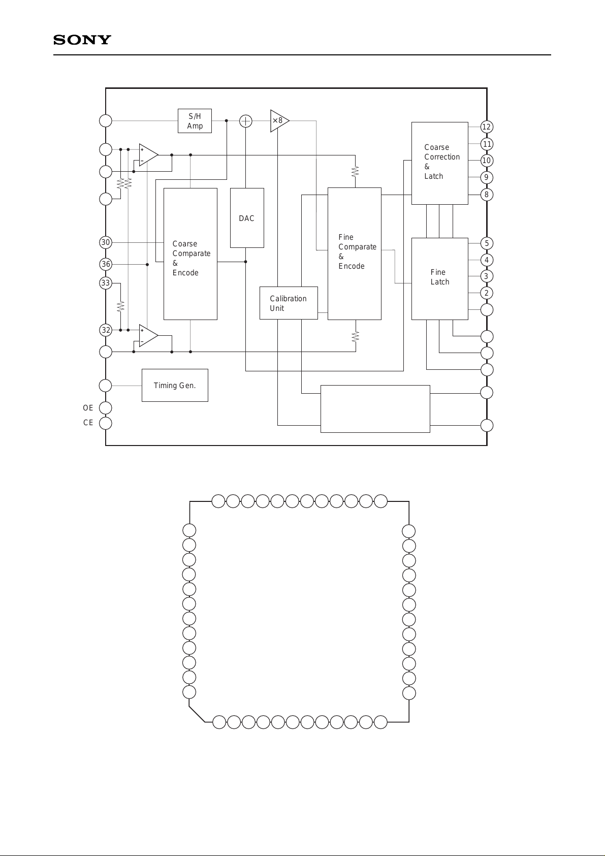
× 8
DAC
Coarse
Comparate
&
Encode
Calibration
Unit
Fine
Comparate
&
Encode
Fine
Latch
Coarse
Correction
&
Latch
Timing Gen.
2
3
4
5
8
9
10
11
12
15
18
19
20
22
23
24
27
38
42
1
A
Auto
Calibration Pulse
Generator
D9
D8
D7
D6
D5
D4
D3
D2
D1
D0 (LSB)
MINV
LINV
TESTMODE
CAL
RESET
31
VRT
VRTC
VRTS
VRMC
VIN
BE
VRBS
VRB
VRBC
CLK
OE
CE
S/H
Amp
30
36
33
32
28
29
–
+
CE
OE
CLK
AV
DD
MINV
LINV
TESTMODE
AV
DD
AVSS
RESET
TIN
TO
TSTR
VIN
TS
AV
DD
AVSS
CAL
AVDD
AT
AV
DD
AVSS
DVDD
DVSS
BE
AV
DD
AV
SS
VRBS
VRB
VRBC
VRMC
VRTC
VRT
VRTS
AV
DD
AV
SS
D1
D2
D3
D4
DV
SS
DV
DD
D5
D6
D7
D8
D9
D0
2
3
4
5
6
7
8
9
10
11
12
13
14
15
16
17
18
19
20
21
22
23
24
25
26
27
28
29
30
40
39
38
37
36
35
34
31
32
33
41
42
43
44
45
46
47
48
1
Pin Configuration
Block Diagram
AA
AA
AA
A
A
A
A
A
A
A
A
A
A
A
A
A
AA
AA
AA
AAAA
– 3 –
CXD3300R
Pin Description
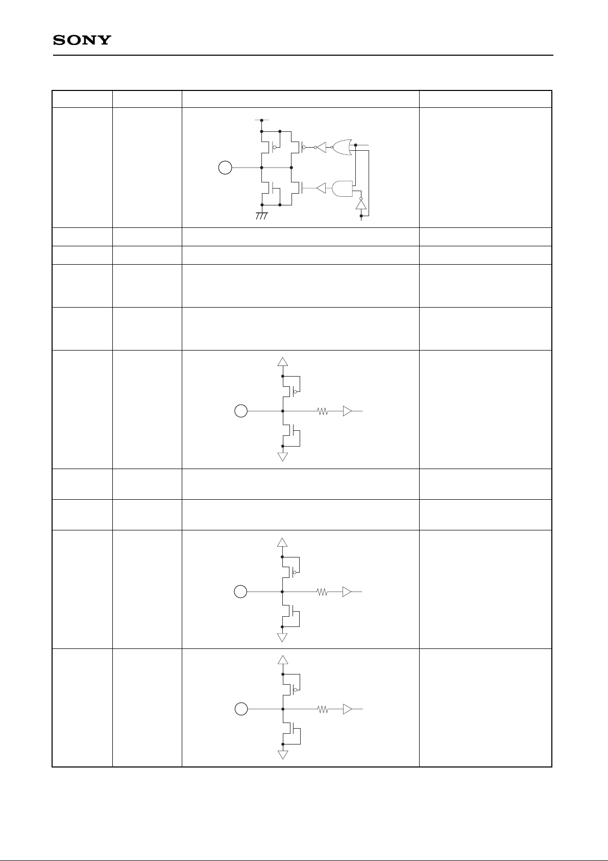
Pin No. Symbol Equivalent circuit Description
1 to 5
8 to 12
D0 to D9
6, 48 DVSS
7, 47 DVDD
13 TO
14 TIN
D0 (LSB) to D9 (MSB)
output.
Digital VSS.
Digital VDD.
Test pin.
High impedance when
TS = High.
Test signal input.
Normally fixed to AVDD or
AVSS.
15 RESET
Calibration circuit reset and
startup calibration restart.
18
TESTMODE
Test mode.
High: Output state
Low: Output fixed
16, 25, 34,
41, 46
AVSS Analog VSS.
17, 21, 26, 35,
40, 43, 45
AVDD
Analog VDD.
DVDD
DVSS
AVDD
AVSS
15
AVDD
AVSS
18
19 LINV
Output inversion.
High: D0 to D8 are
inverted and output.
Low: D0 to D8 are
normal output.
AVDD
AVSS
19
– 4 –
CXD3300R
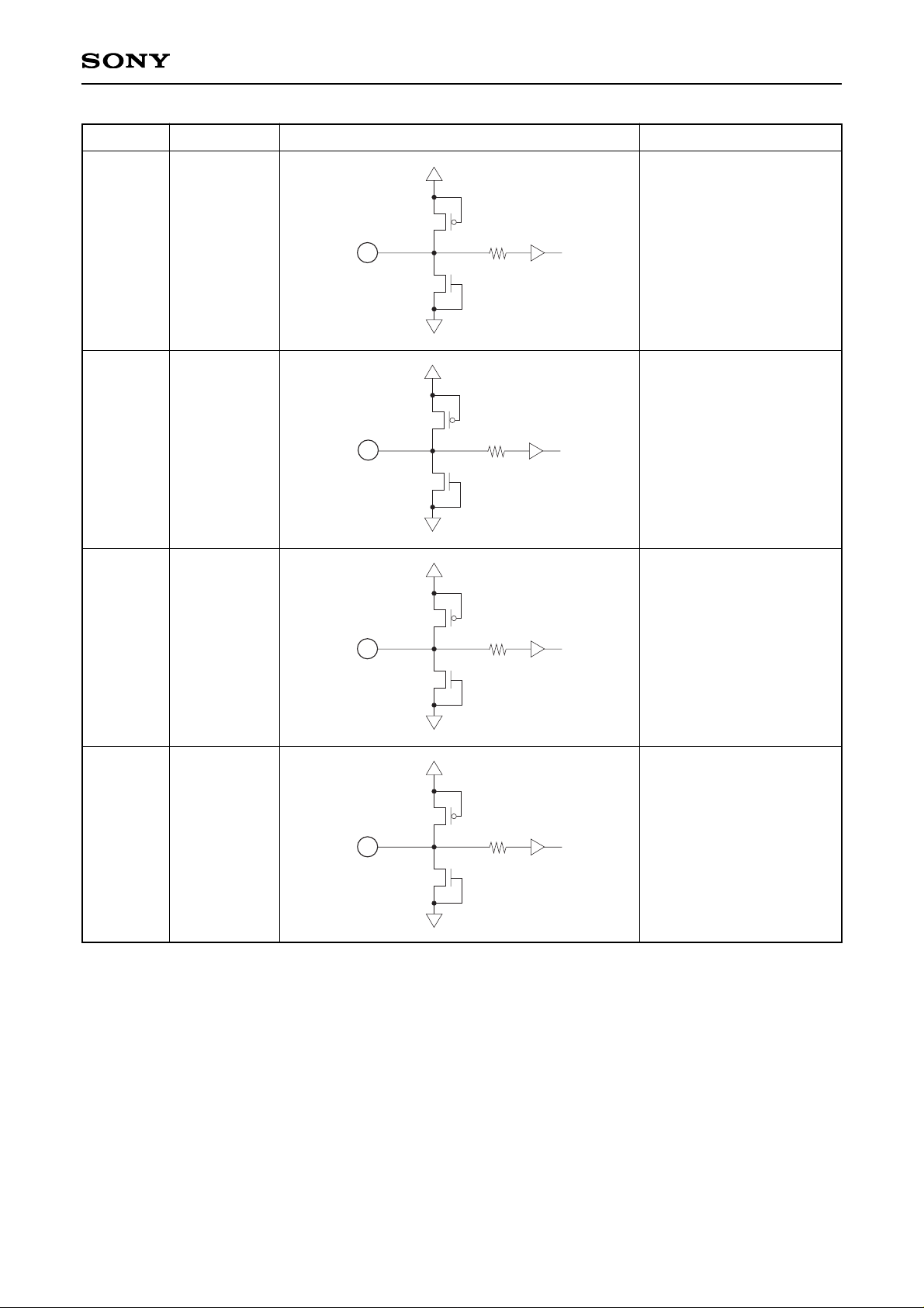
Pin No. Symbol Equivalent circuit Description
20
MINV
Output inversion.
High: D9 is inverted and
output.
Low: D9 is normal output.
AVDD
AVSS
20
22
CLK
Clock.
AVDD
AVSS
22
23
OE
D0 to D9 output enable.
Low: Output state
High: High impedance
state
AVDD
AVSS
23
24
CE
Chip enable.
Low: Active state
High: Standby state
AVDD
AVSS
24
– 5 –
CXD3300R
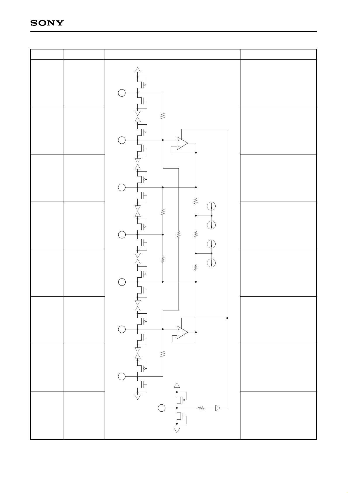
Pin No. Symbol Equivalent circuit Description
Self-bias.
(Reference top)
27
VRTS
Reference top.
28
VRT
Reference top output.
29 VRTC
Reference middle output.
30 VRMC
Reference bottom output.
31 VRBC
Reference bottom.
32 VRB
Self-bias.
(Reference bottom)
33 VRBS
Bias enable.
36
BE
AVDD
AVSS
AVDD
AVSS
AVDD
AVSS
AVDD
AVSS
AVDD
AVSS
AVDD
AVSS
AVDD
AVSS
AVDD
AVSS
27
28
33
32
29
30
31
36
– 6 –
CXD3300R
Pin No. Symbol Equivalent circuit Description
37
TSTR
Test signal input.
Normally fixed to AVDD or
AVSS.
44
AT
Test signal input.
High impedance when
TS = High.
38
VIN
Analog input.
42
CAL
Calibration pulse input.
39
TS
Test signal input.
Normally fixed to AVDD.
AVDD
AVSS
38
AVDD
AVSS
42
 Loading...