
查询CXD3220供应商
CXD3220R
IEEE1394 Link/T ransaction Layer Controller LSI for SBP-2
Description
The CXD3220R is a Link/Transaction Layer LSI
conforming to the IEEE1394 serial bus standard.
It is mainly used when connecting the IEEE1394
digital I/F to a storage device such as a hard disk,
DVD-ROM, CD-ROM or tape streamer.
Data transfer conforms to the SBP-2 protocol.
This LSI utilizes Apple Computer's Fire Wire
technology.
100 pin LQFP (Plastic)
Features
• Conforms to IEEE1394 serial bus standard
• Conforms to SBP-2 (serial bus protocol-2)
• Compatible with bidirectional data transfer of
computer peripherals
• Compatible with 1394 transfer rate at 100/200Mbps
• Dedicated Asynchronous data transfer
• High-speed data transfer through the use of an
ADP (automatic data pipe) circuit
• Cycle master function
• Direct connection to 1394 Phy chip
• Large capacity FIFO
Data transfer FIFO 532 quadlets
Asynchronous Transmit FIFO 24 quadlets
Asynchronous Receive FIFO 39 quadlets
Applications
Digital interface for computer peripheral
Absolute Maximum Ratings (Ta = 25°C)
• Supply voltage VDD VSS – 0.5 to +4.6 V
• Input voltage VI VSS – 0.5 to VDD + 0.5 V
• Output voltage VO VSS – 0.5 to VDD + 0.5 V
• Operating temperature
Topr –20 to +75 °C
• Storage temperature
Tstg –55 to +150 °C
Recommended Operating Conditions
• Supply voltage VDD 3.0 to 3.6 V
• Operating temperature
Topr –20 to +75 °C
Structure
Silicon gate CMOS IC
Sony reserves the right to change products and specifications without prior notice. This information does not convey any license by
any implication or otherwise under any patents or other right. Application circuits shown, if any, are typical examples illustrating the
operation of the devices. Sony cannot assume responsibility for any problems arising out of the use of these circuits.
– 1 –
E97320-PS

CXD3220R
Contents
1. Block Diagram............................................................................................................................................... 3
2. Pin Configuration........................................................................................................................................... 4
3. Pin Description.............................................................................................................................................. 5
4. Electrical Characteristics............................................................................................................................... 8
4-1. DC Characteristics................................................................................................................................. 8
4-2. AC Characteristics ................................................................................................................................. 8
4-3. Input/Output Capacitance ...................................................................................................................... 8
4-4. Timing Definition .................................................................................................................................... 9
5. System Configuration Example................................................................................................................... 10
5-1. System Block Diagram......................................................................................................................... 10
5-2. System Connection Diagram ............................................................................................................... 11
6. Asynchronous Communication.................................................................................................................... 12
6-1. CPU I/F ................................................................................................................................................ 12
6-2. CFR...................................................................................................................................................... 15
6-3. Asynchronous Packet Transmission.................................................................................................... 25
6-4. Asynchronous Packet Reception......................................................................................................... 28
6-5. CXD3220R Data Format...................................................................................................................... 33
6-6. Self-ID Packet Reception Error Processing......................................................................................... 43
7. ADP (Asynchronous Data Pipe).................................................................................................................. 44
7-1. Built-in FIFO......................................................................................................................................... 44
7-2. Transport Data I/F................................................................................................................................ 44
7-3. ADP....................................................................................................................................................... 47
7-4. ADP Structure and Functions............................................................................................................... 49
7-5. ADP Setting.......................................................................................................................................... 51
8. Link-Phy Communication ............................................................................................................................ 58
8-1. Link-Phy Interface Specifications......................................................................................................... 58
8-2. Communication.................................................................................................................................... 58
– 2 –
2
4
DATA [0:3]
CTL [0:1]
LREQ
2
4
CORE
PHY
1
LPS
1
1
1
SYSCLK
1
1
CXD3220R
ADP
(Async Transaction Control,
Packetize according to SBP2)
asynchronous transmit FIFO
Transport
Data IF
Control
1
1
1
1
16
DeMux
Asynchronous
asynchronous recieve FIFO
1
1
Resolver
Control Registers
1
1
7
CPU I/F
16
1
1
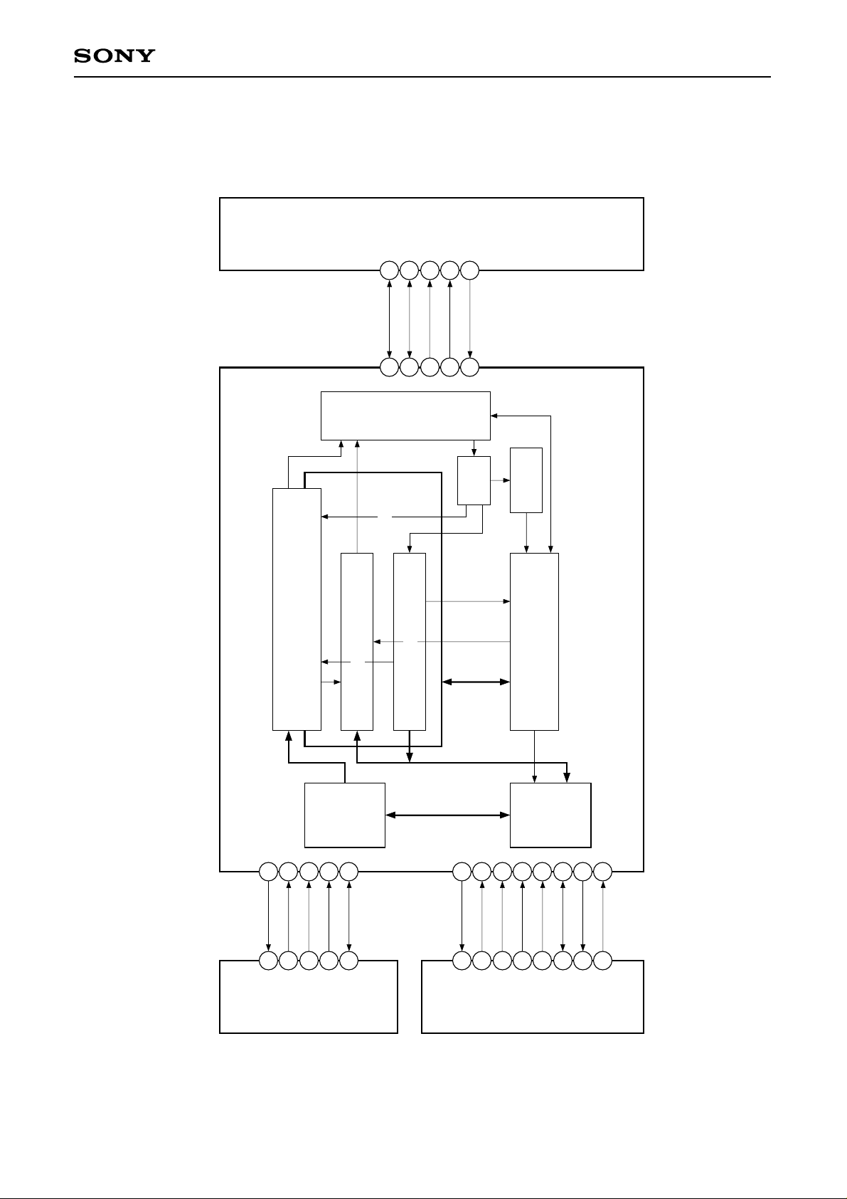
1. Block Diagram
XSAC
SDRQ
1
1
XHRD
XHWR
1
Decoder
SD [0:15]
1
16
– 3 –
XINT
1
XCS
1
XWR
1
XRD
1
Local
A [0:6]
D [0:15]
7
16
Processor
XRESET
XWAIT
1
1

2. Pin Configuration
CXD3220R
VDD
VSS
SD13
SD14
SD15
SDRQ
XSAC
TEST21
TEST22
TEST23
TEST24
X8/16
SS
V
XWAIT
XINT
XCS
ADDRESS0
ADDRESS1
ADDRESS2
ADDRESS3
ADDRESS4
ADDRESS5
ADDRESS6
DATA0
DATA1
76
77
78
80
81
82
83
84
85
86
87
88
89
90
91
92
94
95
96
97
98
99
100
79
93
75
SD12
74
SD11
73
SD10
72
SD9
71
SD8
70
SD7
69
SD6
68
SD5
67
SD4
66
SD3
65
SD2
64
SD1
63
SS
XHRD
SD0
V
62
61
60
XHWR
59
TEST20
XRESET
57
58
TEST19
TEST18
55
56
TEST17
54
TEST16
TEST15
53
SS
DD
V
V
5152
50
TEST14
49
TEST13
48
TEST12
47
TEST11
46
TEST10
45
TEST9
44
LREQ
43
TEST8
42
SYSCLK
41
TEST7
40
CTL0
39
CTL1
38
SS
V
37
D0
36
D1
35
D2
34
D3
33
TEST6
32
RSVD0
31
RSVD1
RSVD2
30
RSVD3
29
LPS
28
VSS
27
VDD
26
3
DATA2
4
DATA3
5
DATA4
DATA5
1
2
SS
DD
V
V
6
7
DATA6
8
DATA7
9
10
DATA8
DATA9
12
11
DATA10
13
14 15
SS
V
DATA11
16
DATA13
DATA12
DATA14
18
17
DATA15
19
XRD
21
20
XWR
TEST0 (BIST)
23
22
24
TEST2 (TDI)
TEST1 (TCK)
25
TEST4 (TD0)
TEST5 (VST)
TEST3 (TENA1)
– 4 –

3. Pin Description
CXD3220R
Pin
No.
1
2
3
4
5
6
7
8
9
10
11
12
13
14
15
Symbol I/O
VDD
VSS
DATA2
DATA3
DATA4
DATA5
DATA6
DATA7
DATA8
DATA9
DATA10
DATA11
VSS
DATA12
DATA13
Power Supply
—
GND
—
CPU I/F I/O data bit 2
I/O
CPU I/F I/O data bit 3
I/O
CPU I/F I/O data bit 4
I/O
CPU I/F I/O data bit 5
I/O
CPU I/F I/O data bit 6
I/O
CPU I/F I/O data bit 7
I/O
CPU I/F I/O data bit 8
I/O
CPU I/F I/O data bit 9
I/O
CPU I/F I/O data bit 10
I/O
CPU I/F I/O data bit 11
I/O
GND
—
CPU I/F I/O data bit 12
I/O
CPU I/F I/O data bit 13
I/O
Description
16
17
18
19
20
21
22
23
24
25
26
27
28
29
30
31
32
33
DATA14
DATA15
XRD
XWR
TEST0
TEST1
TEST2
TEST3
TEST4
TEST5
VDD
VSS
LPS
RSVD3
RSVD2
RSVD1
RSVD0
TEST6
CPU I/F I/O data bit 14
I/O
CPU I/F I/O data bit 15
I/O
CPU I/F read signal
I
I
—
—
—
—
—
—
—
—
O
—
—
—
—
—
0: read
CPU I/F write signal
0: write
Test pin
Test pin
Test pin
Test pin
Test pin
Test pin 2
∗1
∗1
∗1
∗1
∗1
∗2
Power supply
GND
Phy I/F Link power status signal (High level when XRESET input = low)
Reserved
Reserved
Reserved
Reserved
Test pin
∗3
∗3
∗3
∗3
∗1
∗1
The test pins should be used open.
∗2
Connect the test pin 2 to GND.
∗3
RSVD0 to 3 should be used open.
– 5 –

CXD3220R
Pin
No.
34
35
36
37
38
39
40
41
42
43
44
45
46
47
48
49
50
Symbol I/O
D3
D2
D1
D0
VSS
CTL1
CTL0
TEST7
SYSCLK
TEST8
LREQ
TEST9
TEST10
TEST11
TEST12
TEST13
TEST14
Phy I/F data bus bit 3
I/O
Phy I/F data bus bit 2
I/O
Phy I/F data bus bit 1
I/O
Phy I/F data bus bit 0
I/O
GND
—
Phy I/F control bus bit 1
I/O
Phy I/F control bus bit 0
I/O
Test pin
—
Phy I/F system clock (49.195MHz)
I
Test pin
—
Phy I/F request signal
O
Test pin
—
Test pin
—
Test pin
—
Test pin
—
Test pin
—
Test pin
—
∗1
∗1
∗1
∗1
∗1
∗1
∗1
∗1
Description
51
52
53
54
55
56
57
58
59
60
61
62
63
64
65
VDD
VSS
TEST15
TEST16
TEST17
TEST18
TEST19
TEST20
XRESET
XHWR
XHRD
SD0
VSS
SD1
SD2
Power supply
—
GND
—
Test pin
—
Test pin
—
Test pin
—
Test pin
—
Test pin
—
Test pin
—
Master reset signal
I
Transport data I/F data write enable signal
I
Transport data I/F data read enable signal
I
Transport data I/F data bus bit 0
I/O
GND
—
Transport data I/F data bus bit 1
I/O
Transport data I/F data bus bit 2
I/O
∗1
∗1
∗1
∗1
∗1
∗1
0: Active; 1: Non-active
0: Non-active; 1: Active
0: Non-active; 1: Active
66
SD3
67
SD4
∗1
The test pins should be used open.
Transport data I/F data bus bit 3
I/O
Transport data I/F data bus bit 4
I/O
– 6 –

CXD3220R
Pin
No.
68
69
70
71
72
73
74
75
76
77
78
79
80
81
82
83
84
85
86
Symbol I/O
SD5
SD6
SD7
SD8
SD9
SD10
SD11
SD12
VDD
VSS
SD13
SD14
SD15
SDRQ
XSAC
TEST21
TEST22
TEST23
TEST24
Transport data I/F data bus bit 5
I/O
Transport data I/F data bus bit 6
I/O
Transport data I/F data bus bit 7
I/O
Transport data I/F data bus bit 8
I/O
Transport data I/F data bus bit 9
I/O
Transport data I/F data bus bit 10
I/O
Transport data I/F data bus bit 11
I/O
Transport data I/F data bus bit 12
I/O
Power supply
—
GND
—
Transport data I/F data bus bit 13
I/O
Transport data I/F data bus bit 14
I/O
Transport data I/F data bus bit 15
I/O
Transport data I/F data request signal
O
Transport data I/F acknowledge signal
I
—
—
—
—
Test pin
Test pin
Test pin
Test pin
∗1
∗1
∗1
∗1
Description
87
88
89
90
91
92
93
94
95
96
97
98
99
100
X8/16
VSS
XWAIT
XINT
XCS
ADDRESS0
ADDRESS1
ADDRESS2
ADDRESS3
ADDRESS4
ADDRESS5
ADDRESS6
DATA0
DATA1
CPU I/F I/O data bus select signal
I
—
O
O
I
I
I
I
I
I
I
I
I/O
I/O
0: 8 bits; 1:16 bits
GND
CPU I/F wait signal active when XCS = 0,
high impedance when XCS = 1
CPU I/F interrupt signal
0: Active; 1: Non-active
CPU I/F chip select signal
0: Active; 1: Non-active
CPU I/F address bus bit 0
CPU I/F address bus bit 1
CPU I/F address bus bit 2
CPU I/F address bus bit 3
CPU I/F address bus bit 4
CPU I/F address bus bit 5
CPU I/F address bus bit 6
CPU I/F I/O data bit 0
CPU I/F I/O data bit 1
∗1
The test pins should be used open.
– 7 –

CXD3220R
4. Electrical Characteristics
4-1. DC Characteristics (Ta = 25°C, VSS = 0V)
Item Symbol Conditions Min. Typ. Max. Unit
VIH
All input pins
0.7VDD
V
Input voltage
VIL
VOH
VOL
All input pins
Output pins excluding
D [3:0], CTL [1:0], LREQ
IOH = –4mA
IOL = 4mA
VDD – 0.4
0.2VDD
0.4
V
V
V
Output voltage
VOH
IOH = –8mA
VDD – 0.4
V
D [3:0], CTL [1:0], LREQ
Input leak current
Output leak
current
VOL
II1
II2
IIL
IOZ
ICC1
IOL = 8mA
SD [15:0], D [3:0], CTL [1:0]
Normal input pins
XHRD, XHWR, XRD, XRESET, XSAC,
XWR
XWAIT (for high impedance state)
VIN = Vss or VDD
For ADP operation VDD = 3.3V
–40
–10
–240
–40
–100
90
0.4
40
10
–40
40
120
V
µA
µA
µA
µA
mA
Power supply
ICC2
For ADP not operation VDD = 3.3V
50
70
mA
4-2. AC Characteristics (VDD = 3.0 to 3.6V)
Item Applicable pins Symbol
Input setup
Input hold
SD [15:0], SDRQ, XSAC,
XHRD, XHWR
Output delay
Input setup
D [3:0], CTL [1:0]
Input hold
Output delay
Input setup
Input hold
Output delay
D [3:0], CTL [1:0], LREQ
ADDRESS [6:0], DATA [15:0],
XCS, XWR, XRD
DATA [15:0], XWAIT
4-3. Input/Output Capacitance
Item Symbol Conditions Min. Typ. Max. Unit
Input capacitance
Output capacitance
CIN
COUT
All input pins
All input pins
Tsu1
Th1
Td1
Tsu2
Th2
Td2
Tsu3
Th3
Td3
Reference clock
Conditions
Min. Typ. Max. Unit
Refer to 7-2. Transport data I/F write timing and
Transport data I/F read timing
5
CL = 10pFSYSCLK
2
215
Refer to 6-1. ATF/CFR write timing and ATF/CFR
read timing
9
11
ns
ns
ns
pF
pF
I/O capacitance
CI/O
D [3:0], CTL [1:0], SD [15:0]
– 8 –
11
pF

4-4. Timing Definition
Reference clock
Output
CXD3220R
Input
Tsu Th
Td
– 9 –
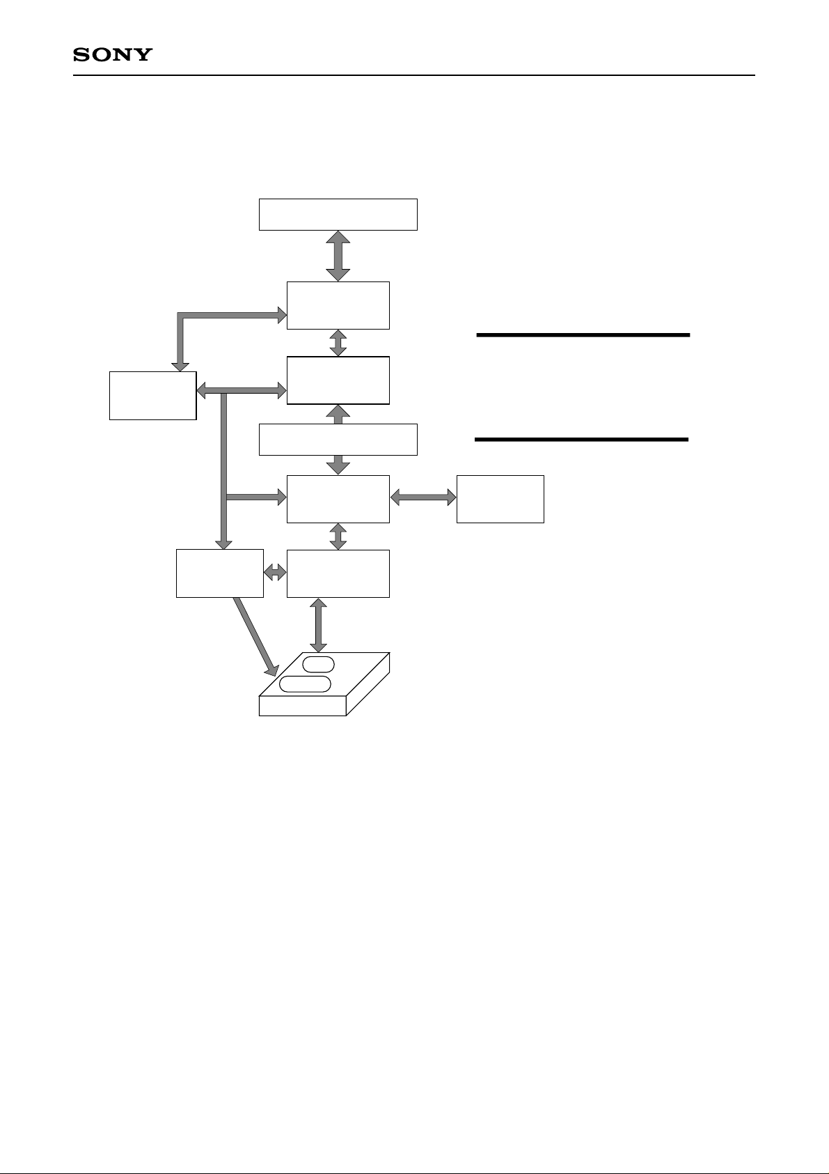
5. System Configuration Example
5-1. System Block Diagram
CXD3220R
1394 Serial BUS
CPU
Servo Control
DSP
PHY Chip
LINK Controller
Transport Data I/F
ENDEC/ECC
Disk R/W Logic
OP
Actuator
1394 PHY Layer
1394 LINK Layer
Buffer DRAM
Storage Device
– 10 –
2
4
DATA [0:3]
CTL [0:1]
LREQ
2
4
CORE
PHY
1
LPS
1
1
1
SYSCLK
1
1
CXD3220R
ADP
(Async Transaction Control,
Packetize according to SBP2)
asynchronous transmit FIFO
Transport
Data IF
Control
1
1
1
1
16
DeMux
Asynchronous
asynchronous recieve FIFO
1
1
Resolver
Control Registers
1
1
7
CPU I/F
1
1
XHWR
XSAC
SDRQ
1
1
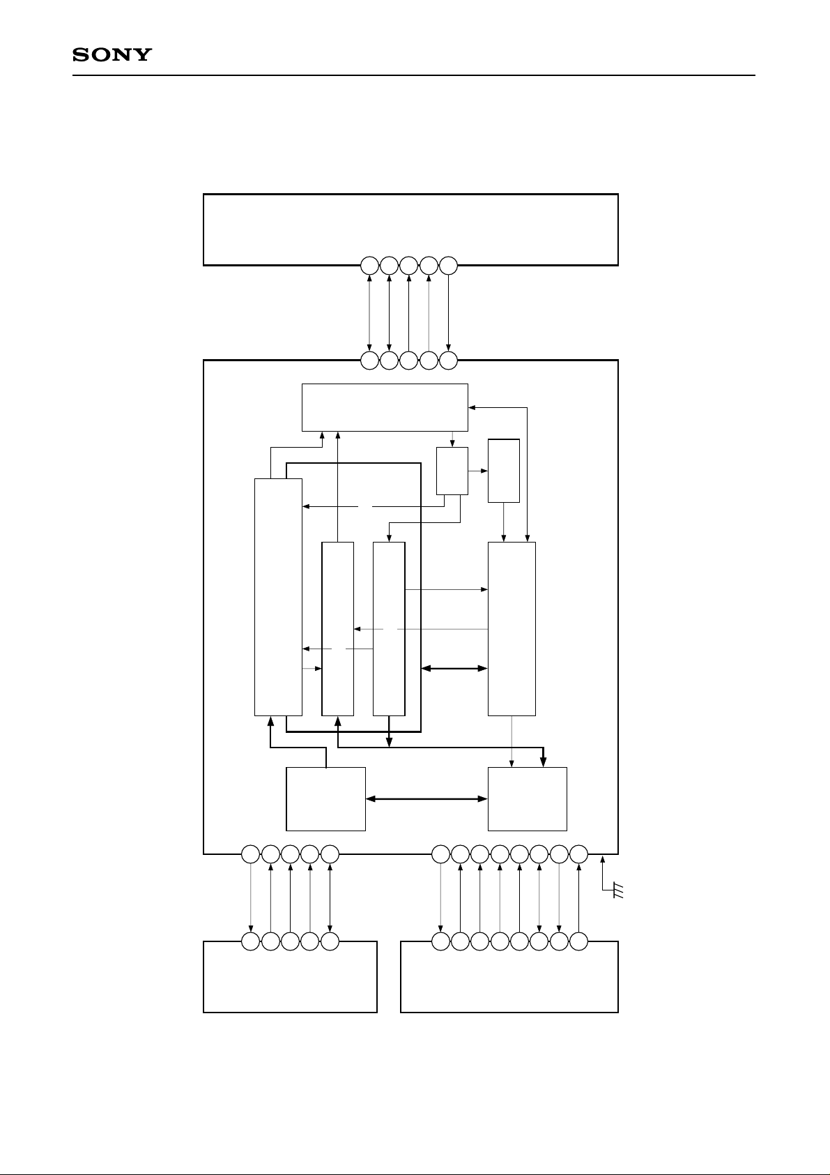
• CPU Interface....8bit
• Transport Data Interface....16bit
5-2. System Connection Diagram
XHRD
1
1
Decoder
SD [0:15]
16
– 11 –
XINT
1
XCS
1
XWR
1
XRD
1
Local
A [0:6]
D [0:7]
8 8
7
Processor
XRESET
XWAIT
1
X8/16
1

CXD3220R
6. Asynchronous Communication
6-1. CPU I/F
The CPU I/F controls data communication between the external CPU and the CXD3220R ATF/ARF/CFR∗1,
respectively.
Communications between the CPU and CXD3220R include:
1) CPU writes data to ATF → Asynchronous packet transmit
2) CPU reads data in ARF → Asynchronous packet receive
3) CPU writes data to CFR → mode, header data setting
4) CPU reads data in CFR → internal status, header data read
5) CXD3220R informs CPU of an interrupt event with an interrupt signal
The CXD3220R supports 16-bit and 8-bit CPU I/F.
The ATF/ARF/CFR built in the CXD3220R have a 32-bit structure, so all bits can not be accessed with one
access. The target address must be accessed two consecutive times for 16 bits and four consecutive times for
8 bits.
The roles played by the signals communicated between the CXD3220R and the external CPU are given
bellow.
Data [15:0] in/out Data for writing to or reading from specified address
ADDRESS [6:0] in Address for writing or reading data
Data destination (CFR or FIFO) and data breakpoint (Write or Confirm) are
discriminated according to the address
XCS in Access enable from host bus (low active)
XWR in Data write enable signal (low: write)
XRD in Data read enable signal (low: read)
XWAIT out Indicates access (read or write) completed to specified address (low active)
XINT out Interrupt signal. Indicates some kind of interrupt when low
Type of interrupt and mask specified by CFR
X8/16 in CPU I/F data bus switching
High: 16 bits; low: 8 bits
∗1
ATF (Asynchronous Transmit FIFO), ARF (Asynchronous Receive FIFO), CFR (Configuration Register)
In the CXD3220R, the ATF has the capacity of 24 quadlets and the ARF has the capacity of 39 quadlets.
– 12 –
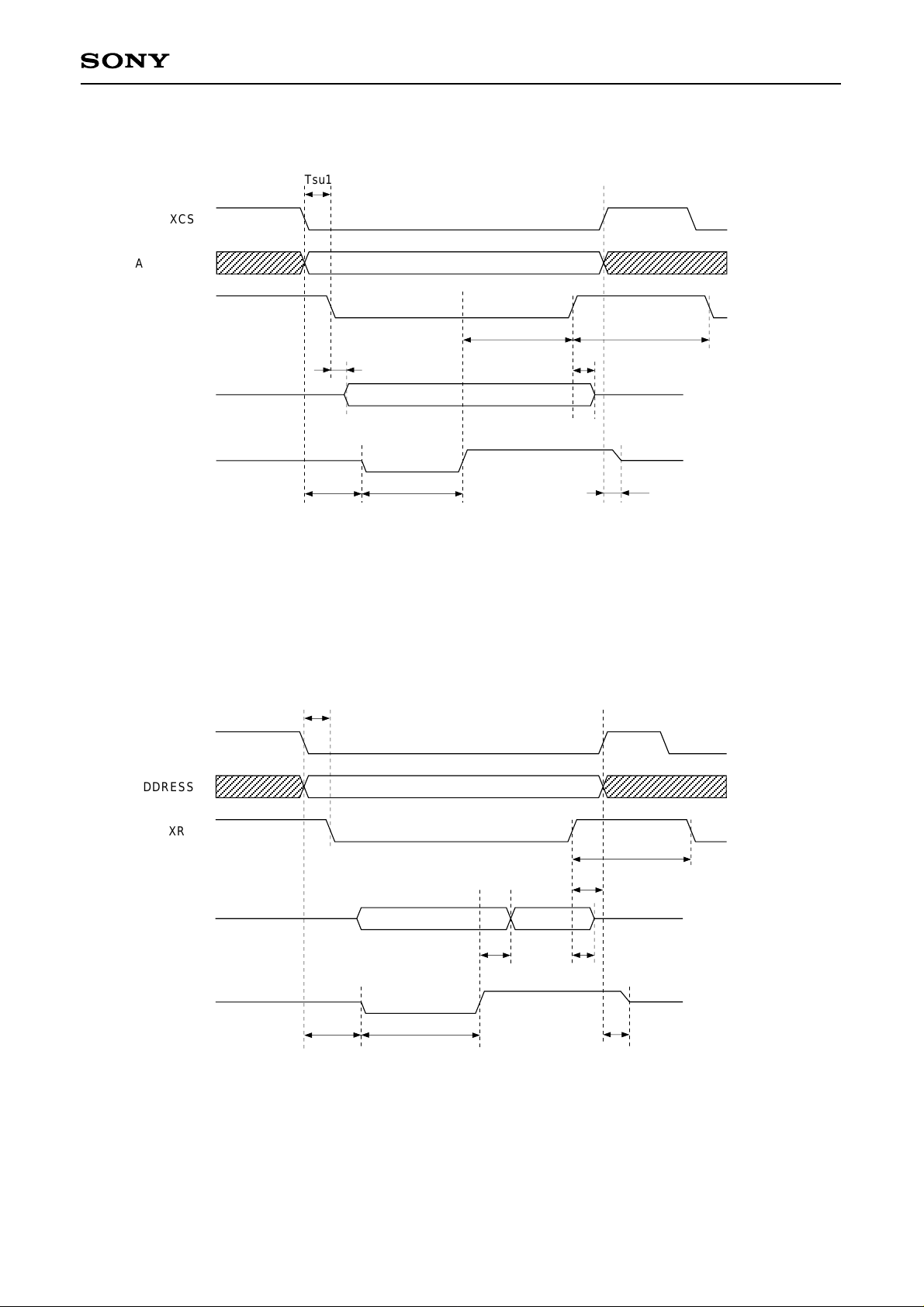
Writing Timing to ATF/CFR
XCS
ADDRESS
XWR
Tsu1
Th1
CXD3220R
Twrh
DATA
XWAIT
Tsu1 5nsec min, Tsu3 13nsec max, Th1 5nsec min, Twrh 60nsec min
Twait 100nsec max, Th2 8nsec max, Th3 14nsec max, Th4 5nsec min
Read Timing from ARF/CFR
XCS
ADDRESS
Tsu1
Tsu3
Th4
valid
Th3Th2 Twait
XRD
DATA
XWAIT
Trdh
Th5
invalid
Tsu1 5nsec min, Th1 3nsec max, Trdh 60nsec min
Twait 270nsec max, Th2 16nsec max, Th3 8nsec max, Th4 14nsec max, Th5 5nsec min
valid
Th2Th1
Th4Th3 Twait
– 13 –
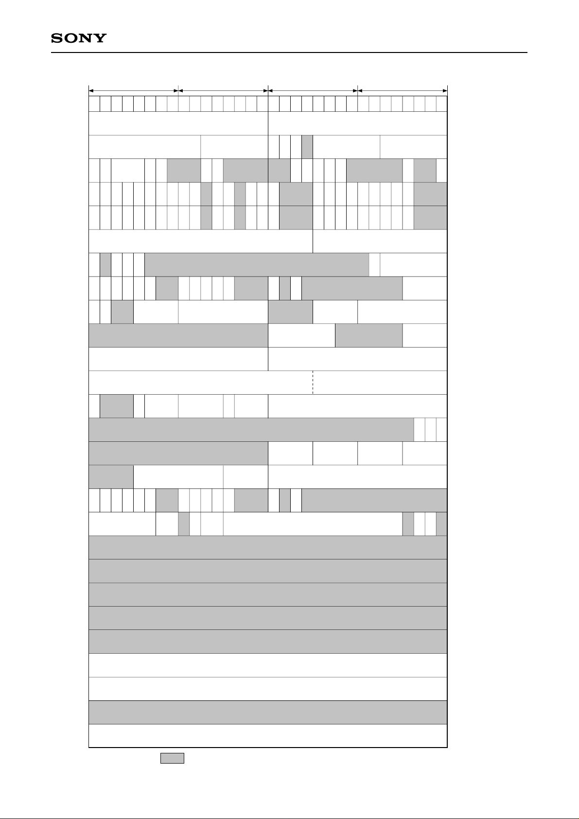
Configuration Register (CFR) Address Map
A [1:0]
00
31302928272625242322212019181716151413121110987654321
01 10 11
CXD3220R
0
00
04
08
0C
10
14
18
1C
20
24
28
2C
idVal
RxSld
Int
PhyInt
Int
PhyInt
EnSnoop
arfFull
arfAFull
WrPhy
RdPhy
Version
BusNumber NodeNumber
BsyCtrl
PhRRx
PhRRx
BusRst
BusRst
TxEn
TxRdy
FairGap
TxRdy
FairGap
RxEn
RxDta
RxDta
EndSlf
CmdRst
EndSlf
CmdRst
RstTx
RcvAckRcvAck
RstRx
ITStk
ITStk
CycleNumber CycleOffset
FrGp
ArbGp
regRW
arf
arfDc
4There
AEmpty
arf
arfEmpty
atfFull
arf
atfAFull
4Avail
atf
AEmpty
segment_offset_Low segment_offset
ATStk
ATStk
atfEmpty
SntRj
SntRj
Revision
NodeSum CFMContID
CySrc
AckCtl
CyMasEn
CySt
CySec
CySt
CySec
CyTEn
CyDne
CyDne
CyPnd
CyPnd
CyLst
CyLst
HdrErr
HdrErr
Clear
root
TCErr
TCErr
ATF
Status
Power
CyMas
AIDT16
ARF
Clear
tLabel priority
segment_base_HigedestinationID
ADPStADPSt
CyAbFail
CyAbFail
DiffGap
PhyDataRxRegPhyAdRxRegPhyRegDataPhyRegAd
StrSid
ADPErrADPErr
ADPCmpADPCmp
SIGapCnt
ATAck
Version
Node Address
Control
LPS
Interrupt
Interrupt Mask
Cycle Timer
Diagnostics
Async Status
Phy Chip Access
ADP1
ADP2
ADP3
30
34
38
3C
40
44
70
AFull
adprf
adprf
adprfFull
testpin_select
4There
adprfDc
dn
AEmpty
adprf
adprf
max_payload
spd
retry_interval
Empty
test_
control
adptfFull
page_size
P
err rcode ack-i ack-o
retry_limit split_timeout
adptf
testiso
adptf
ram
test
4Avail
adptf
AEmpty
Clear
ADPT
Clear
Empty
adptf
AFull
ATF Write (first quadlet of the packet)
ADPR
testout
xfer_length
reset
ADP
Arf/XAtf
ADP4
ADP Control
ADPgo
ADPstop
ADP Status
Transacton Timeout
ADP FIFO Status
TEST Mode
FIFOChg
74
ATF Write/ARF read
78
7C
∗
The shaded areas ( ) are reserved and can not be used.
ATF Write (confirm write)
– 14 –

CXD3220R
6-2. CFR (Configuration Register)
This is a memory space to store the status information, operation mode and packet header information in the
chip. Read/write with the external CPU can be performed via the CPU I/F.
The address map and register contents are shown below.
Register Description
1) Version/Revision Register
These registers have the CXD3220R version/revision written in them.
The register address is 00h; they are read only, and the default value is 3220_0000h.
Bit Name
31 to 16
15 to 0
Version
Revision
CXD3220R version number
CXD3220R revision number
Function
2) Node Address Register
These registers are used to monitor root/cycle master status and the total number of nodes connected, and so
on.
The register address is 04h and the initial value is FFFF_0000h.
Only the bus number is for read/write, and the other registers are normally for read only, but the Diagnostic
register can be read/write by setting regRW to "1".
Bit Name
31 to 22
21 to 16
15
14
Bus Number
Node Number
root
Power Status
Bus number of connected bus
Node number of this link
Root/not root for this link
1: root; 0: not root
Cable power status for this mode
1: CPS on; 0: CPS off
Function
13
11 to 6
5 to 0
CyMas
NodeSum
CFMcontID
Whether or not this link is cycle master
1: cycle master; 0: not
Total number of connected nodes. The value becomes "0" when an error
occurs in the Self ID phase. This value is fixed when the Interrupt register
EndSlf bit becomes "1" from "0".
The Phy-ID value of the contender is loaded.
However, when the CXD3220R node has an ability to become the contender
and this LSI has the Phy-ID value larger than the loaded value, the CXD3220R
itself is the contender. This value is fixed when the Interrupt register EndSlf
bit becomes "1" from "0".
– 15 –

3) Control Register
These registers perform settings for the CXD3220R basic operations.
The register address is 08h; they are for read/write, and the initial value is C600_2A01h.
CXD3220R
Bit Name
31
30
29 to 27
26
25
21
20
13
12
11
idVal
RxSld
BsyCtrl
TxEn
RxEn
RstTx
RstRx
AIDT16
AckCtl
CyMasEn
Function
Receives packet from the address set in the Node Address register and
packet at bus number "3FFh" node number "3Fh" when "1". Receives packet
at bus number "3FFh" node number "3Fh" only when "0".
Validates reception of Self ID packet when "1". Non-valid when "0".
(Fixed at "1" in the CXD3220R)
Controls Busy status of input packet
000 = Returns Busy according to normal Busy/retry protocol when necessary.
(Fixed at "000" in the CXD3220R)
Transmitter does not transmit Arbitration and packet when "0".
Receiver does not receive packet when "0".
Sync resets transmitter when "1".
This bit is cleared automatically. (Do not use for normal operation.)
Sync resets receiver when "1".
This bit is cleared automatically. (Do not use for normal operation.)
Selects SD bus width. 8 bits when "0" and 16 bits when "1".
Controls the Ack code that is sent back when a packet is received for which
Tcode = 0, 1 (write request quadlet/block).
0: Ack code = 1 (complete), 1: Ack code = 2 (pending)
The Cycle Master function operates if the CXD3220R becomes Root when "1".
10
Incrementation of the cycle number and reset of Cycle Offset are performed
CySrc
with Cycle In when "1". Incrementation is performed with Cycle Offset when
"0". (This is always set to "0" internally for this link.)
9
3
0
CyTEn
StrSid
LPS
Validates Cycle Offset increment when "1".
(This is always set to "1" internally for this link.)
Takes received Self ID packet in at the ARF when "1".
Does not take received Self ID packet in to the ARF when "0".
The LPS pin is high when "1".
The LPS pin is low when "0".
– 16 –

CXD3220R
4) Interrupt and Interrupt-Mask Registers
These registers combine the Interrupt register, which informs the CPU I/F of changes in the CXD3220R status,
and the Interrupt-Mask register, which masks the Interrupt register.
The address of the Interrupt register is 0Ch, and when the regRW bit is "0", bits other than Int bit and ADPErr
bit are cleared by writing "1". When the regRW bit is "1" all bits are for read/write.
The address of the Interrupt-Mask register is 10h and it is for read/write. When "1" is written to the
corresponding bit, the interrupt becomes valid; when "0" is written, it becomes invalid.
The initial value for both registers is 0000_0000h. The Interrupt OR corresponding to the bit where "1" is
written in the Interrupt-Mask register becomes the INT bit, resulting in the XINT output signal.
And the XINT output signal becomes valid when "1" is written to the Interrupt-Mask register INT bit; when "0" is
written, invalid.
Bit Name
31
30
29
28
27
26
25
24
23
22
20
19
Int
PhyInt
PhyRegRx
BusRst
FairGap
TxRdy
RxDta
CmdRst
EndSlf
RcvAck
ITStk
ATStk
Function
All interrupt OR results and their interrupt mask bits.
Phy Interrupt was received from Phy chip.
Data was received from Phy to Phy register.
Bus Reset was received from Phy.
Fair Gap received from Phy.
Transmitter is able to transmit. "0" when a packet is transmitted; "1" when an
Ack code is fixed.
Receiver has received a correct packet. A packet is not loaded in the ARF
when the Self-ID packet is received if the Control register Strsid is set to "0"
and when the Response packet is received at the ADP circuit for ADP
operation. However, RxDta Interrupt is set.
Receiver has received a packet addressed to CSR RESET_START register.
Indicates that Self ID phase has completed.
Ack code was received.
Transmitter detected wrong data in Isochronous FIFO during Isochronous
transmit. (Always set to "0" in this IC)
Transmitter detected wrong data in Asynchronous FIFO during Asynchronous
transmit.
17
16
15
11
10
SntRj
HdrErr
TCErr
CySec
CycSt
9
8
7
6
CycDne
CycPnd
CycLst
CyAbFail
Receiver transmitted Busy Ack for a packet transmitted to this node because
received FIFO is full.
Receiver detected Header CRC error in the packet transmitted to this note.
Transmitter detected wrong tCode data in transmitted FIFO.
Cycle Timer register Cycle Number upper 7 bits were incremented.
(This is generated almost every second when Cycle Timer is valid.)
Transmitter/Receiver transmitted/received Cycle Start packet.
After transmit or receive of Cycle Start packet, Fair Gap was detected on the
bus. This means that the Isochronous cycle is complete.
Cycle Timer register Cycle Offset is "0". Stays as is until Isochronous cycle is
complete.
When not Cycle Master, Cycle Timer completed two cycles without receiving
Cycle Start packet.
Failure of Cycle Start packet transmission Arbitration.
– 17 –

CXD3220R
Bit Name
5
4
3
ADPSt
ADPCmp
ADPErr
The ADP has started.
The ADP has completed.
An error has occurred during ADP processing. In order to clear ADPErr bit,
write "1" to this bit after "1" is written to ADP Control register ADPreset bit.
Function
5) Cycle Timer Registers
These registers are composed of the 24.576MHz clock cycle Cycle Offset and the 125µs in its host, and the
Cycle Number that counts one second. The value of all nodes are regulated by the Cycle Master node.
The register address is 14h; it is for read/write, and the initial value is 0000_0000h.
Bit Name
Function
The upper 7 bits count seconds (1Hz) and the lower 13 bits count the
31 to 12
CycleNumber
Isochronous cycle (8kHz = 125µs). The values are controlled by Control
register Cycle Master and Cycle Timer Enable.
Counts the system clock (24.576MHz). The Cycle Number is incremented
11 to 0
CycleOffset
when this counter completes one cycle. The value is controlled by Control
register Cycle Master and Cycle Timer Enable.
6) Diagnostic Register
This register controls or monitors the CXD3220R status.
The register address is 18h and the initial value is 0000_0000h.
Only the EnSp bit and regRW bit are for read/write; other bits are for read/write when the regRW bit is "1" and
for read only when it is "0".
Bit Name
31
30
29
28
27
6
5 to 0
EnSnoop
BsyF
ArbGp
FrGp
regRW
DiffGap
SIGapCnt
Receives all packets on the bus regardless of receiver address and format
when "1". Invalid when "0".
Ack to be sent back next is "Ack_BusyB" when "1".
Ack to be sent back next is "Ack_BusyA" when "0".
Bus is in idle state due to Arbitration Reset Gap.
Bus is in idle state due to Fair Gap.
Almost all registers are for read/write when "1".
"1" when there is dispersion in Gap count values in received Self ID. This
value is fixed when the Interrupt register EndSlf bit becomes "1" from "0".
The value is entered when all Gap count values in received Self ID are the
same. "00h" when bus reset is generated.
Function
– 18 –

CXD3220R
7) Asynchronous Transmit and Received FIFO Status Registers
These registers can monitor and control the ATF/ARF statuses.
The register address is 1ch and the initial value is 0428_0000h.
Only the Clear ATF bit and Clear ARF bit are for read/write; other bits are for read/write when the regRW bit is
"1" and read only when it is "0".
Bit Name
31
30
29
28
27
26
23
22
21
20
19
15
13
3 to 0
ARFFull
ARFAFull
ARF4Th
ARFDc
ARFAEmpty
ARFEmpty
ATFFull
ATFAFull
ATF4Avail
ATFAEmpty
ATFEmpty
ClearATF
ClearARF
ATAck
Function
The ARF is full when "1" and receive is not possible.
The ARF can receive only one more quadlet when "1".
The ATF can write more than four quadlets of data when "1".
This is the control bit for reading a packet from ARF, and is "1" only for the
first and last quadlets of the packet.
Only one more quadlet of data is written in the ARF when "1".
The ARF is empty when "1" and there is no data to be read.
The ATF is full when "1" and write is not possible.
Only one more quadlet can be written in the ATF when "1".
More than four quadlets of data can be written in the ATF when "1".
The ATF has only one more quadlet of data not transmitted when "1".
The ATF is empty when "1" and there is no data for transmit.
Sync reset of ATF when "1" (Self Clear).
Sync reset of ARF when "1" (Self Clear).
Value of received Ack code. This is fixed when the TxRdy bit becomes "1"
from "0" and the fixed value is maintained till the next Act code is received.
8) Phy Chip Access Registers
These registers are used for read/write of the contents of the Phy chip Phy register connected to the
CXD3220R.
The register address is 20h and the initial value is 0000_0000h.
Bit Name
31
30
27 to 24
23 to 16
11 to 8
7 to 0
RdPhy
WrPhy
PhyRegAd
PhyRegData
PhyAdRxReg
PhyDataRxReg
The CXD3220R requests read to the address set in PhyRgAd via the Phy I/F
when "1".
The CXD3220R requests write to the address set in PhyRgAd via the Phy I/F
when "1".
Sets the read/write address of the connected Phy chip Phy register.
Value of data for write to address specified by PhyRegAd.
Value of the read Phy register address during read.
Value of the read Phy register data during read.
Function
– 19 –

9) ADP1 Registers
These registers are used to set the ADP.
The register address is 24h and the initial value is 0000_0000h.
CXD3220R
Bit Name
Indicates the Transaction Label and is used in a pair with the response
15 to 10
tLabel
packet to that request packet. (Do not use the tLabel set with ADP for
packets transmitted from the ATF.)
Indicates the priority level of the packet.
3 to 0
priority
In the case of a value other than "0", the transmitter uses priority Arbitration
for this packet.
10) ADP2 Registers
These registers are used for setting of the ADP.
The register address is 28h and the initial value is 0000_0000h.
Bit Name
31 to 16
15 to 0
destinationID
segment_base
_High
The bus number of the destination of the packet is represented with 10 bits,
while the node number is represented with 6 bits.
For a continuous area (segment_base_High, segment_base_Low and,
depending on the case, segment_offset), this indicates the address of the
address space of the destination node.
Function
Function
11) ADP3 Registers
These registers are used for setting of the ADP.
The register address is 2Ch and the initial value is 0000_0000h.
All 32 bits are at segment_base_Low when in Mode0 or 1.
In Mode2, the lower bit (page_size + 8) is at segment_offset, while the upper bit is at segment_base_Low.
Mode0 and Mode1
Bit Name
31 to 0
segment_base
_Low
For a continuous area (segment_base_High, segment_base_Low), this
indicates the address of the address space of the destination node. This
address must be in word units when the Control register AIDT16 = "1" in Mode1.
Function
Mode2
Bit Name
Function
For 3 continuous areas (segment_base_High, segment_base_Low,
31 to b
segment_base
_Low
segment_offset), this indicates the address of the address space of the
destination node. This address must be in word units when the Control
register AIDT16 = "1".
In the case of Mode2 that supports transfer by page_table, this indicates the
(b – 1) to 0
segment_offset
lower bit of the first address of the element. It also sets the segment_offset
value of ORB.
b = (page_size + 8)
– 20 –
 Loading...