

Sony CXD3059AR Schematics

CXD3059AR
CD Digital Signal Processor with Built-in RF Amplifier and Digital Servo + Digital High & Bass Boost
Description
The CXD3059AR is a digital signal processor LSI for CD
players. This LSI incorporates a RF amplifier and digital servo,
high & bass boost, 1-bit DAC and analog low-pass filter.
Features
• All digital signal processing during playback is performed with
a single chip
• Highly integrated mounting possible due to a built-in RF
amplifier
RF Block
• Supports 4× speed playback CD
• RF system equalizer
• Supports pickup built-in RF summing amplifier
• Gain level switch
• TE balance adjustment function
Digital Signal Processor (DSP) Block
• Supports CAV (Constant Angular Velocity) playback
• Frame jitter free
• 0.5× to 4× speed continuous playback possible
• Allows relative rotational velocity readout
• Supports variable pitch playback
• The bit clock, which strobes the EFM signal, is generated by
the digital PLL.
• EFM data demodulation
• Enhanced EFM frame sync signal protection
• Refined super strategy-based powerful error correction
C1: double correction, C2: quadruple correction
Supported during 4× speed playback
• Noise reduction during track jumps
• Auto zero-cross mute
• Subcode demodulation and subcode-Q data error detection
• Digital spindle servo
• 16-bit traverse counter
• Asymmetry correction circuit
• CPU interface on serial bus
• Error correction monitor signal, etc. output from CPU
interface
• Servo auto sequencer
• Fine search performs track jumps with high accuracy
• Digital audio interface outputs
• Digital level meter, peak meter
• Bilingual compatible
• VCO control mode
• CD TEXT data demodulation
Digital Servo (DSSP) Block
• Microcomputer software-based flexible servo control
• Offset cancel function for servo error signal
• Auto gain control function for servo loop
• E:F balance, focus bias adjustment functions
• Surf jump function supporting micro two-axis
• Tracking filter: 6 stages,
Focus filter: 5 stages
Digital Filter, DAC and Analog Low-pass Filter Blocks
• Digital dynamic bass boost and high boost
Bass Boost: 4th-order IIR 24dB/Oct
+10dB/+14dB/+18dB/+22dB
High Boost: Second-order IIR 12dB/Oct
+4dB/+6dB/+8dB/+10dB
• Independent turnover frequency selection possible
Bass Boost: 125Hz/160Hz/200Hz
High Boost: 5kHz/7kHz
• Digital dynamics (compressor)
Volume increased by +5dB at low level
• 8× oversampling digital filter
(attenuation: 61dB, ripple within band: ±0.0075dB)
• Digital signal output possible after boost
• Serial data format selectable from (output)
20 bits/18 bits/16 bits (rearward truncation, MSB first)
• Digital attenuation: –∞, –60 to +6dB, 2048 steps (linear)
• Soft mute
• Digital de-emphasis
• High-cut filter
Applications
CD players
Structure
Silicon gate CMOS IC
Absolute Maximum Ratings (Ta = 25°C)
• Supply voltage 1 V
• Input voltage 1 V
• Output voltage 1 V
• Supply voltage 2 IOV
• Input voltage 2 V
• Output voltage 2 V
• Storage temperature
• Supply voltage difference
Recommended Operating Conditions
• Supply voltage 1 V
• Supply voltage 2 IOV
• Operating temperature
I/O Pin Capacitance
• Input capacitance C
• Output capacitance C
• I/O capacitance C
Note) Measurement conditions V
120 pin LQFP (Plastic)
DD, XVDD VSS – 0.5 to +3.5 V
I1VSS – 0.3 to VDD + 0.3 V
O1VSS – 0.3 to VDD + 0.3 V
DD0 to 2, AVDD0 to 5
I2IOVSS – 0.3 to IOVDD + 0.3 V
O2IOVSS – 0.3 to IOVDD + 0.3 V
Tstg –55 to +150 °C
IOV
SS, AVSS, XVSS – VSS
DD – VDD –0.3 to +0.3 V
XV
IOV
DD, AVDD, XVDD – VDD
DD, XVDD 2.5 ± 0.2 V
DD0 to 2, AVDD0 to 5
Topr –20 to +75 °C
I 7 (Max.) pF
O 7 (Max.) pF
I/O 7 (Max.) pF
IOV
SS – 0.5 to +4.5 V
–0.3 to +0.3 V
–0.3 to +0.3 V
DD, AVDD, XVDD < 2.3V)
(IOV
3.3 ± 0.3 V
DD = VI = 0V
f
M = 1MHz
Sony reserves the right to change products and specifications without prior notice. This information does not convey any license by
any implication or otherwise under any patents or other right. Application circuits shown, if any, are typical examples illustrating the
operation of the devices. Sony cannot assume responsibility for any problems arising out of the use of these circuits.
– 1 –
E03736-PS
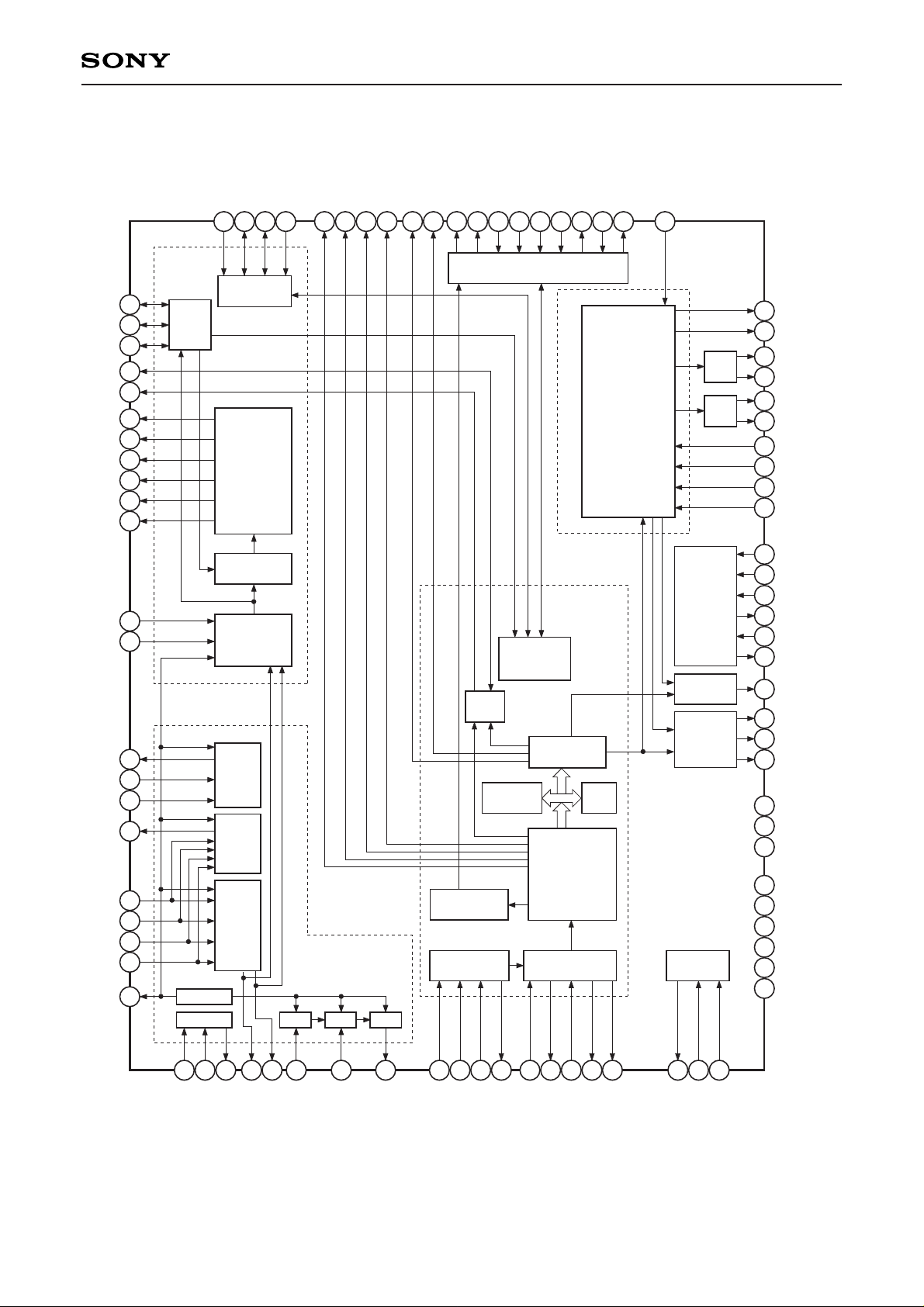
Block Diagram
SSTP
COUT
ATSK
SCLK
GFS
XUGF
WFCK
EMPH
WDCK
C2PO
SCOR
SENS
CLOK
XLAT
DATA
EXCK
SBSO
SQCK
SQSO
CXD3059AR
SYSM
MIRR
DFCT
FOK
LOCK
MDP
SFDR
SRDR
TFDR
TRDR
FFDR
FRDR
TEI
FEI
TEO
FEO
VC
SERVO
Block
MIRR
DFCT
FOK
E
F
A
B
C
D
SERVO
Interface
PWM
Generator
SERVO
DSP
A/D
Converter
TE
FE
Sub Code
Processor
SUM
RFamp Block
Asymmetry
Corrector
VC
APC ATT EQ AMP
Digital
CLV
Error
Corrector
CPU Interface
Bass Boost Block
CD Signal
Prosessor
Block
Servo
Auto
Sequencer
D/A
Interface
EFM
Demodulator
Digital
PLL
32K
RAM
DAC
LPF
LPF
Clock
Generator
Digital
OUT
Selector
DC/DC
Convertor
LMUT
RMUT
AOUT2
VREFR
VREL
AOUT1
EMPHI
LRCKI
PCMDI
BCKI
XTACN
XTSL
XTAI
XTAO
VCTL
VPCO
DOUT
BCK
PCMD
LRCK
XRST
TES1
TEST
AVDD0 to 5
AVSS0 to 5
IOVDD0 to 2
IOVSS0 to 2
V
DD
V
SS
PD
LD
PDSENS
RFDCO
AC_SUM
EQ_IN
RFC
RFACO
BIAS
RFACI
– 2 –
ASYI
ASYO
CLTV
FIFO
FILI
PCO
XPCK
DDCR
DDVRSEN
DDVROUT
Pin Configuration
CXD3059AR
LMUT
NC
XTSL
IOV
SS
XTACN
SQSO
SQCK
SBSO
EXCK
XRST
SYSM
DATA
V
XLAT
CLOK
V
DD
SENS
SCLK
ATSK
WFCK
XUGF
XPCK
GFS
C2PO
SCOR
V
DD
C4M
WDCK
COUT
NC
RMUT
0
DD
IOV
NC
2
DD
AV
AOUT2
VREFR
2
SS
AV
1
SS
AV
VREFL
AOUT1
1
DD
AV
DD
XV
XTAI
XTAO
XVSSNC
2
SS
IOV
TES1
737481828384 7576777888 87 86 85 79808990
91
92
93
94
0
95
96
97
98
99
100
101
102
103
SS
104
105
106
107
108
109
110
111
112
113
114
115
116
117
118
119
120
TEST
DOUT
70 69 68 67 63646566 61627172
2
DD
IOV
EMPHI
EMPH
DD
BCK
PCMD
VSSLRCK
LRCKI
V
PCMDI
60
BCKI
59
NC
58
DDCR
57
AV
56
DDVRSEN
55
DDVROUT
54
AV
53
PCO
52
FILI
51
FILO
50
CLTV
49
AV
48
VCTL
47
VPCO
46
ASYO
45
ASYI
44
BIAS
43
AV
42
RFACI
41
RFACO
40
AV
39
RFC
38
NC
37
PD
36
LD
35
EQ_IN
34
AC_SUM
33
PDSENS
32
RFDCO
31
AV
SS
5
DD
5
SS
3
DD
3
SS
4
DD
4
2 3 4 5 6 7 8 9 10 11 12 13 14 15 16 17 18 19 20 21 22 23 24 25 26 27 28 29 301
MIRR
DFCT
FOK
MDP
SSTP
1
SS
IOV
SFDR
SRDR
TFDR
TRDR
SS
V
LOCK
FFDR
FRDR
1
DD
IOV
0
DD
AV
0
SS
AV
NC
F
E
TEI
FEI
TEO
FEO
VC
A
B
C
D
NC
– 3 –
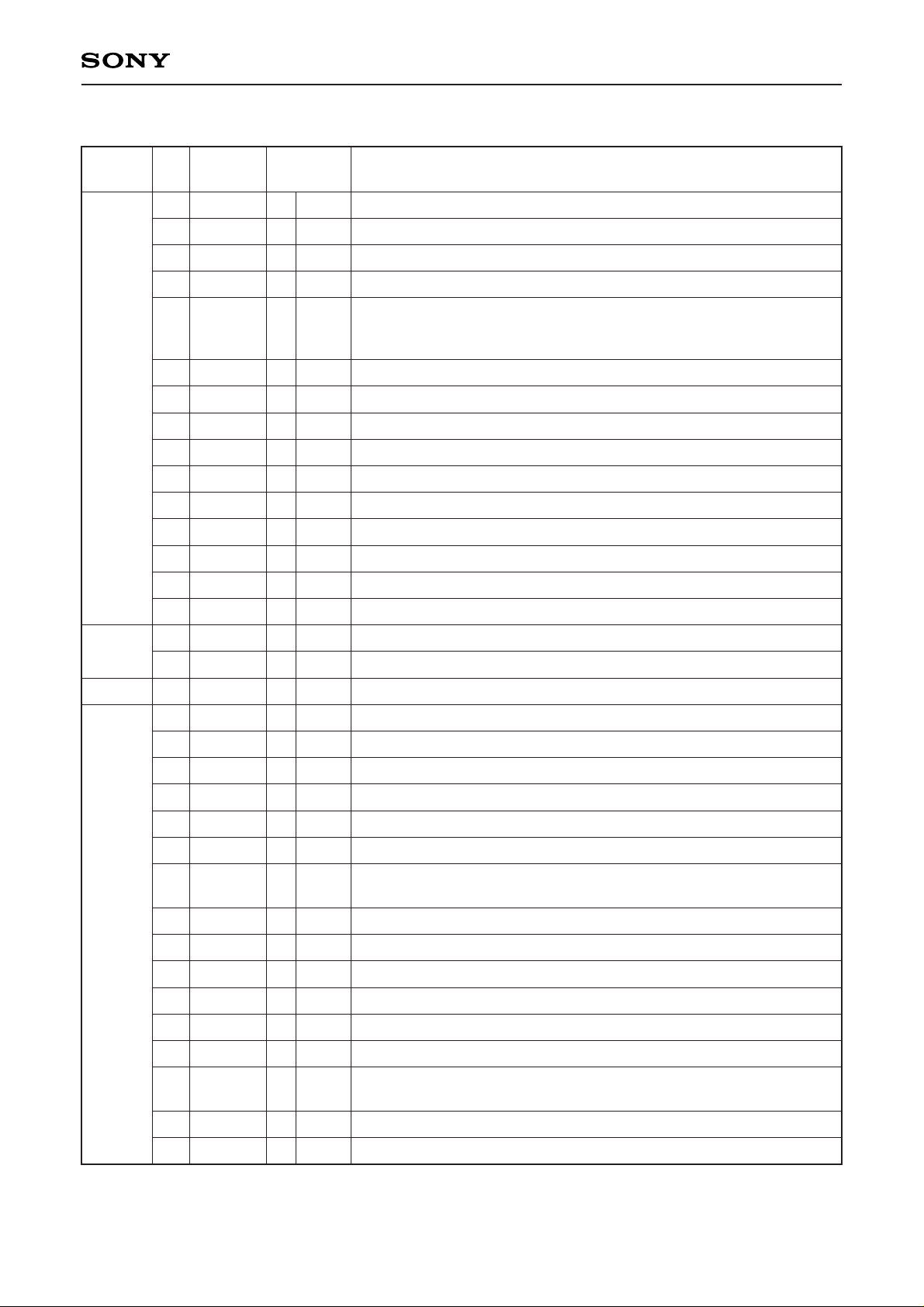
Pin Description
CXD3059AR
Power
supply
Digital
I/O = 3.3V
Internal =
2.5V
Pin
Symbol I/O Description
No.
1
MIRR
2
DFCT
3
FOK
SS
4
V
I/O
I/O
I/O
—
1, 0
1, 0
1, 0
—
Mirror signal input/output.
Defect signal input/output.
Focus OK signal input/output.
Internal digital GND.
GFS is sampled at 460Hz; when GFS is high , this pin outputs a high
5
LOCK
I/O
1, 0
signal. If GFS is low eight consecutive
samples, this pin outputs low. Or this pin inputs when LKIN = "1".
6
7
8
9
10
11
12
13
14
MDP
SSTP
IOVSS1
SFDR
SRDR
TFDR
TRDR
FFDR
FRDR
O
I
—
O
O
O
O
O
O
1, Z, 0
—
1, 0
1, 0
1, 0
1, 0
1, 0
1, 0
Spindle motor servo control output.
Disk innermost detection signal input.
I/O digital GND.
Sled drive output.
Sled drive output.
Tracking drive output.
Tracking drive output.
Focus drive output.
Focus drive output.
A/D
3.3V
—
RFamp
3.3V
15
16
17
18
19
20
21
22
23
24
25
26
27
28
29
30
31
IOVDD1
AVDD0
AVSS0
NC
E
F
TEI
TEO
FEI
FEO
VC
A
B
C
D
NC
AVDD4
—
—
—
—
I
I
I
O
I
O
I/O
I
I
I
I
—
—
I/O digital power supply.
—
Analog power supply.
—
Analog GND.
—
—
E signal input.
F signal input.
Tracking error signal input to DSSP block.
Tracking error signal output from RF amplifier block.
Focus error signal input to DSSP block.
Focus error signal output from RF amplifier block.
Center voltage output from RF amplifier block.
Center voltage input to DSSP block by command switch.
A signal input.
B signal input.
C signal input.
D signal input.
—
Analog power supply.
—
32
33
34
RFDCO
PDSENS
AC_SUM
I/O
I
O
Analog
RFDC signal output.
RFDC signal input to DSSP block by command switch.
Reference voltage pin for PD.
RFAC summing amplifier output.
– 4 –
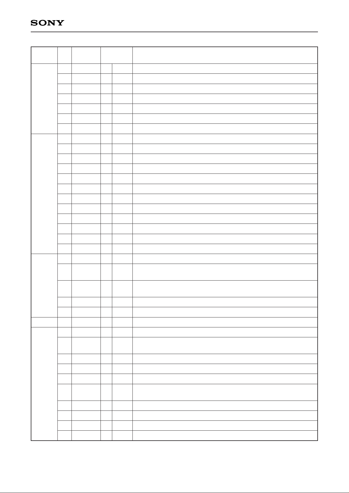
CXD3059AR
Power
supply
RFamp
3.3V
ASYM
3.3V
Pin
Symbol I/O Description
No.
35
36
37
38
39
40
41
42
43
44
45
46
47
48
49
50
EQ_IN
LD
PD
NC
RFC
AVSS4
RFACO
RFACI
AVDD3
BIAS
ASYI
ASYO
VPCO
VCTL
AVSS3
CLTV
I
O
I
—
I
—
O
I
—
I
I
O
O
I
—
I
—
—
—
1, 0
1, Z, 0
—
Equalizer circuit input.
APC amplifier output.
APC amplifier input.
Equalizer cut-off frequency adjustment pin.
Analog GND.
RFAC signal output.
RFAC signal input or EFM signal input.
Analog power supply.
Asymmetry circuit constant current input.
Asymmetry comparator voltage input.
EFM full-swing output. (Low = VSS, High = VDD)
Wide-band EFM PLL charge pump output.
Wide-band EFM PLL VCO2 control voltage input.
Analog GND.
Multiplier VCO1 control voltage input.
DC/DC
3.3V
—
Digital
I/O = 3.3V
Internal =
2.5V
51
52
53
54
55
56
57
58
59
60
61
62
63
64
65
FILO
FILI
PCO
AVDD5
DDVROUT
DDVRSEN
AVSS5
DDCR
NC
BCKI
PCMDI
LRCKl
LRCK
VSS
PCMD
O
I
O
—
O
I
—
I
—
I
I
I
O
—
O
Analog
1, Z, 0
—
—
—
1, 0
—
1, 0
Master PLL (slave = digital PLL) filter output.
Master PLL filter input.
Master PLL charge pump output.
Analog power supply.
DC/DC converter output.
Leave open when not using.
DC/DC converter output voltage monitor pin.
Connect to analog power supply when not using.
Analog GND.
DC/DC converter reset pin.
D/A interface bit clock input.
D/A interface serial data input.
(2's COMP, MSB first)
D/A interface LR clock input.
D/A interface LR clock output. f = Fs
Internal digital GND.
D/A interface serial data output.
(2's COMP, MSB first)
66
67
68
69
BCK
VDD
EMPH
EMPHI
O
—
O
1, 0
1, 0
I
D/A interface bit clock output.
Internal digital power supply.
—
High when the playback disc has emphasis, low it has not.
High when de-emphasis is ON, low when input OFF.
– 5 –
CXD3059AR
Power
supply
Digital
I/O = 3.3V
Internal =
2.5V
—
X'tal
2.5V
Lch
3.3V
Rch
3.3V
Pin
Symbol I/O Description
No.
70
71
72
73
74
75
76
77
78
79
80
81
82
83
84
85
86
IOVDD2
DOUT
TEST
TES1
IOVss2
NC
XVSS
XTAO
XTAI
XVDD
AVDD1
AOUT1
VREFL
AVSS1
AVSS2
VREFR
AOUT2
—
O
—
—
—
O
—
—
O
O
—
—
O
O
I/O digital power supply.
—
1, 0
I
I
Digital Out output.
Test pin. Normally GND.
Test pin. Normally GND.
I/O digital GND.
—
—
Master clock GND.
—
Crystal oscillation circuit output.
I
Crystal oscillation circuit input.
Master clock power supply.
—
Analog power supply.
—
Lch analog output.
Lch reference voltage.
Analog GND.
—
Analog GND.
—
Rch reference voltage.
Rch analog output.
—
Digital
I/O = 3.3V
Internal =
2.5V
87
88
89
90
91
92
93
94
95
96
97
98
99
100
101
AVDD2
NC
IOVDD0
RMUT
LMUT
NC
XTSL
IOVSS0
XTACN
SQSO
SQCK
SBSO
EXCK
XRST
SYSM
—
—
—
O
O
—
—
O
O
Analog power supply.
—
—
I/O digital power supply.
—
1, 0
1, 0
Rch "0" detection flag.
Lch "0" detection flag.
—
Crystal selection input.
I
Low when the crystal is 16.9344MHz;
high when the crystal is 33.8688MHz.
I/O digital GND.
—
I
1, 0
I
1, 0
I
I
I
Oscillation circuit control.
Self-oscillation when high, oscillation stop when low.
Subcode Q 80-bit and PCM peak and level data output.
CD TEXT data output.
SQSO readout clock input.
Subcode P to W serial output.
SBSO readout clock input.
System reset. Reset when low.
Mute input. Muted when high.
102
103
104
D ATA
VSS
XLAT
—
I
I
Serial data input from CPU.
Internal digital GND.
—
Latch input from CPU. The serial data is latched at the falling edge.
– 6 –
CXD3059AR
Power
supply
Digital
I/O = 3.3V
Internal =
2.5V
Pin
Symbol I/O Description
No.
105
106
107
108
109
110
111
112
113
114
115
116
CLOK
VDD
SENS
SCLK
ATSK
WFCK
XUGF
XPCK
GFS
C2PO
SCOR
VDD
I
—
O
I
I/O
O
O
O
O
O
O
—
—
1, 0
1, 0
1, 0
1, 0
1, 0
1, 0
1, 0
1, 0
—
Serial data transfer clock input from CPU.
Internal digital power supply.
SENS output to CPU.
SENS serial data readout clock input.
Anti-shock input/output.
WFCK output.
XUGF output.
Output MNT0, RFCK, SOUT by command switch.
XPCK output.
Output MNT1, SOCK by command switch.
GFS output.
Output MNT2, XROF, XOLT by command switch.
C2PO output.
Output MNT3, GTOP by command switch.
High output when the subcode sync, S0 or S1, is detected.
Internal digital power supply.
4.2336MHz output.
117
C4M
O
1, 0
1/4 frequency-division output of the V16M in CAV-W mode and
variable pitch mode.
118
119
120
WDCK
COUT
NC
O
I/O
—
1, 0
1, 0
Word clock output. f = 2Fs.
GRSCOR output by command switch.
Track number count signal input/output.
—
Notes)
• PCMD is a MSB first, two's complement output.
• GTOP is used to monitor the frame sync protection status. (High: sync protection window released.)
• XUGF is the frame sync obtained from the EFM signal, and is negative pulse. It is the signal before sync
protection.
• XPCK is the inverse of the EFM PLL clock. The PLL is designed so that the falling edge and the EFM
signal transition point coincide.
• The GFS signal goes high when the frame sync and the insertion protection timing match.
• RFCK is derived from the crystal accuracy, and has a cycle of 136µs.
• C2PO represents the data error status.
• XROF is generated when the 32K RAM exceeds the ±28 frame jitter margin.
• C4M is a 4.2336MHz output that changes in CAV-W mode and variable pitch mode.
• FSTO is the 2/3 frequency-division output of the XTAI pin.
• SOUT is the serial data output inside the servo block.
• SOCK is the serial data readout clock output inside the servo block.
• XOLT is the serial data latch output inside the servo block.
– 7 –
Monitor Pin Output Combinations
CXD3059AR
Command bit
SRO1
0
0
0
0
1
MTSL1
0
0
1
1
0
MTSL0
0
1
0
1
0
XUGF
MNT0
RFCK
C4M
SOUT
XPCK
MNT1
XPCK
GSTO
SOCK
Reset Timing when Power on
Power on with XRST pin low.
Set XRST pin high after holding it low 100ns or more to cancel reset.
Output data
GFS
MNT2
XROF
GFS
XOLT
C2PO
MNT3
GTOP
C2PO
C2PO
– 8 –
RF Block Pin Equivalent Circuit
CXD3059AR
Pin
No.
Symbol I/O Equivalent circuit Description
19 E I
20 F I
21 TEI I
19
20
21
VC
Tracking error amplifier input.
VC
Tracking error signal input to DSSP
block.
22 TEO O
23 FEI I
1pF
22
23
1pF
Tracking error amplifier output.
Focus error signal input to DSSP
block.
24 FEO O Focus error amplifier output.
24
25 VC I/O (AVDD4 – AVSS4)/2 voltage output.
25
– 9 –
 Loading...