

Sony CXD1913AQ Datasheet
Digital Video Encoder
Description
The CXD1913AQ is a digital video encoder designed
for video CD, car navigation system and other digital
video applications. The device accepts ITU-R601
compatible Y, Cb, Cr data and also accepts ITUR656-format Y, Cb, Cr data, and the data are
encoded to composite video and separate Y/C video
(S-Video) signal.
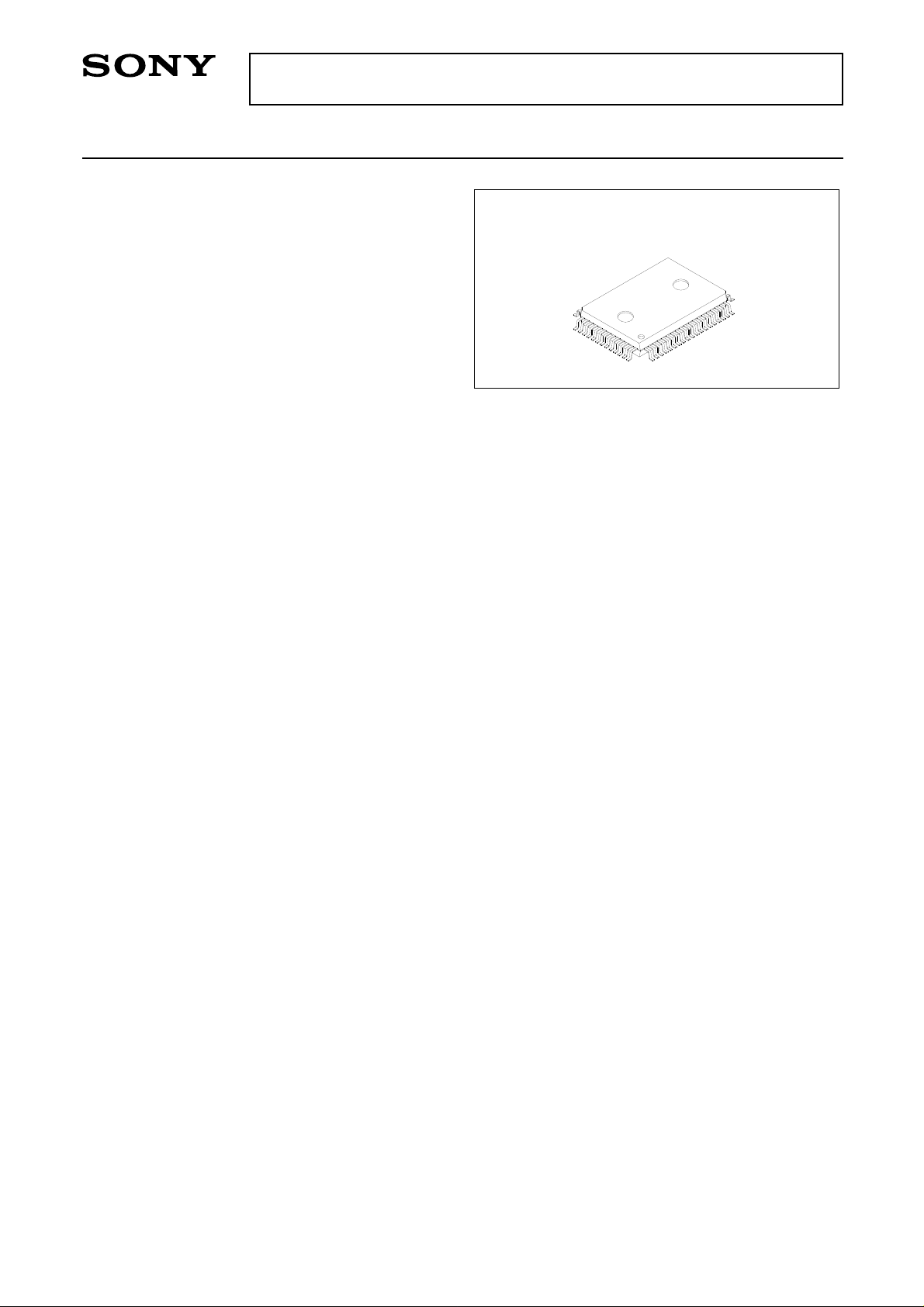
CXD1913AQ
64 pin QFP (Plastic)
Features
• NTSC and PAL encoding mode
• Composite video and separate Y/C video (S-Video)
signal outputs
• 8/16-bit pixel data input mode
• 13.5 Mpps pixel rate
• Interlace and non-interlace supported
• On-chip 100% color bar generator
• 10-bit 3 channels DACs
• Supports I2C bus (400kHz) and SONY SIO
• Closed Caption (Line 21, Line 284) encoding
• VBID encoding
• Monolithic CMOS single 3.3V ± 5% and 5.0V ± 5%
power supplies
• 64-pin plastic QFP package
Absolute Maximum Ratings
• Supply voltage VDD –0.3 to +7.0 V
• Input voltage VI –0.3 to +7.0 V
• Output voltage VO –0.3 to +7.0 V
• Operating temperature Topr –20 to +75 °C
• Storage temperature Tstg –40 to +125 °C
(Vss = 0V)
Recommended Operating Conditions
• Logic supply voltage DVDD 3.3V ± 5%
DVDD 5.0V ± 5%
• Analog supply voltage AVDD 3.3V ± 5%
AVDD 5.0V ± 5%
• Input voltage VIN Vss to VDD V
• Operating temperature Topr 0 to +70 °C
I/O Capacitance
• Input pin CI 11 (Max.) pF
• Output pin CO 11 (Max.) pF
Note) Test conditions: VDD = VI = 0V
fM = 1MHz
Sony reserves the right to change products and specifications without prior notice. This information does not convey any license by
any implication or otherwise under any patents or other right. Application circuits shown, if any, are typical examples illustrating the
operation of the devices. Sony cannot assume responsibility for any problems arising out of the use of these circuits.
– 1 –
E97918-PS

CXD1913AQ
VB
25
Y-OUT
29
DAC
10bit
COMP-O
24
DAC
10bit
Interpolator
CHROMA
Modulator
C-OUT
32
DAC
10bit
VG
26
SYNC Slope
Gen.
IREF
20
VREF
21
TDO
46
TDI
43
TMS
44
TCK
45
TRST
41
54
37 to 39,
XTEST
XTEST1 to 3
Delay
Y
Demultiplex,
6 to 9
1 to 4,
PD0 to 7
U
and
Translator
Level
11 to 18
PD8 to 15
LPF
V
4:4:4
4:2:2 to
interpolator
LPF
1/2
57
PDCLK
BURST FLAG
56
59
VSYNC
SYSCLK
Sub Carrier
CSYNC
and
SYNC Gen.
Timing Controller
60
62
FID
HSYNC
Gen.
51
52
XVRST
F1/XTEST4
(for NTSC)
VBID Encoder
(for NTSC)
Closed Caption Encoder
Controller
SIO
50
49
XCS/SA
SCK/SCL
61
SO
64
XIICEN
48
SI/SDA
55
XRST
Block Diagram
– 2 –
Pin Description
CXD1913AQ
Pin
No.
1
2
3
4
5
6
7
8
9
10
11
12
13
14
15
16
17
Symbol I/O Description
PD7
PD6
I
8-bit pixel data input pins (PD0 to 7).
When control register bit “PIF MODE” = “0”:
I
These are inputs for multiplexed Y, Cb, and Cr signal.
PD5
PD4
VSS
PD3
PD2
I
When control register bit “PIF MODE” = “1”:
I
—
Digital ground
I
8-bit pixel data input pins (PD0 to 7).
When control register bit “PIF MODE” = “0”:
I
These are inputs for Y signal.
These are inputs for multiplexed Y, Cb, and Cr signal.
PD1
PD0
VDD
PD15/TD7
PD14/TD6
I
When control register bit “PIF MODE” = “1”
I
—
Digital power supply
These are inputs for Y signal.
I/O
I/O
8-bit pixel data input pins / Test data bus.
PD13/TD5
PD12/TD4
I/O
When control register bit “PIF MODE” = “0”:
I/O
These inputs are not used.
When control register bit “PIF MODE” = “1”:
PD11/TD3
PD10/TD2
I/O
For test mode, it's used for internal circuit test data bus.
I/O
These are inputs for multiplexed Cb and Cr signal.
Test mode is available only for device bender.
PD9/TD1
I/O
18
19
20
21
22
23
24
25
26
27
28
29
30
31
PD8/TD0
VSS
IREF
VREF
AVDD1
AVSS1
COMP-O
VB
VG
AVDD2
AVSS2
Y-OUT
AVDD3
AVSS3
I/O
—
Digital ground
Reference current output.
O
Connect resistance “16R” which is 16 times output resistance “R”.
Voltage reference input.
I
Sets output full scale value.
—
Analog power supply
—
Analog ground
10-bit D/A converter output.
O
This pin outputs composite signal.
O
Connect to VSS with a capacitor of approximately 0.1µF.
O
Connect to AVDD with a capacitor of approximately 0.1µF.
—
Analog power supply
—
Analog ground
10-bit D/A converter output.
O
This pin outputs luminance (Y) signal.
—
Analog power supply
—
Analog ground
– 3 –
CXD1913AQ
Pin
No.
32
33
34
35
36
37
38
39
40
41
42
Symbol I/O Description
C-OUT
10-bit D/A converter output. This pin outputs chroma (C) signal.
O
Test data bus.
TD10
This pin should be open.
I/O
For test mode, it’s used for internal circuit test data bus.
Test mode is available only for device bender.
VDD
TD9
TD8
XTEST1
XTEST2
XTEST3
VSS
TRST
VDD
Digital power supply
—
Test data bus.
I/O
These pins should be open.
For test mode, it’s used for internal circuit test data bus.
I/O
Test mode is available only for device bender.
I
Test mode control inputs. These pins are pulled up.
I
Normally, these pins should be open.
I
Digital ground
—
Test mode reset input. This pin is pulled up.
I
For power on reset, set “L” for more than 40 clocks (SYSCLK).
Digital power supply
—
43
44
45
46
47
48
49
50
51
52
TDI
TMS
TCK
TDO
VSS
SI/SDA
SCK/SCL
XCS/SA
XVRST
F1/
XTEST4
Test mode control input. This pin is pulled up.
I
Test mode control input. This pin is pulled up.
I
Test mode control input. This pin should be “H” input.
I
Test data bus output. This pin should be open.
O
Digital ground
—
This pin's function is selected by XIICEN (Pin 64).
When XIICEN = “H”, this pin is SONY SIO mode; SI serial data input.
I
When XIICEN = “L”, this pin is I2C bus mode; SDA input/output.
This pin's function is selected by XIICEN (Pin 64).
When XIICEN = “H”, this pin is SONY SIO mode; SCK serial clock input.
I
When XIICEN = “L”, this pin is I2C bus mode; SCL input.
This pin's function is selected by XIICEN (Pin 64). This pin is pulled up.
When XIICEN = “H”, this pin is SONY SIO mode; XCS chip select input.
I
When XIICEN =“L”, this pin is I2C bus mode; SA slave address select input
signal which selects I2C bus slave address.
Vertical sync reset input in active low. This pin is pulled up.
This is used to synchronize external vertical sync and internal vertical sync.
I
When XVRST is “L”, internal digital sync generator is reset according to F1 status.
Valid only for 8-bit mode (control register address 01H bit 4 "PF MODE" = "0").
This pin's function is selected by XTEST (Pin 54).
When XTEST = "H", this pin is F1; field ID input.
I
Field ID during vertical sync reset is indicated.
“H” indicates 1st field. “L” indicates 2nd field.
When XTEST = "L", XTEST4 input.
– 4 –

CXD1913AQ
Pin
No.
53
54
55
56
57
58
59
60
61
62
Symbol I/O Function
VDD
XTEST
XRST
SYSCLK
Digital power supply
—
Test mode control input. This pin is pulled up.
I
Normally, this pin should be open.
System reset input in active low.
I
For power on reset, set “L” for more than 40 clocks (SYSCLK).
System clock input.
I
To generate correct subcarrier frequency, precise 27MHz is required.
Pixel data clock output.
PDCLK
This clock is divided in half from SYSCLK.
O
This is used when 16-bit pixel data mode.
VSS
VSYNC
HSYNC
Digital ground
—
Vertical sync signal output.
O
Horizontal sync signal output.
O
This pin's function is selected by XIICEN (Pin 64).
SO
When XIICEN = “H”, this pin is SONY SIO mode; SO serial out output.
O
When XIICEN = “L”, this pin is not used and output is high impedance.
Field ID output.
When control register bit “FIDS” = “1”:
FID
O
“L” indicates 1st field, “H” indicates 2nd field.
When control register bit “FIDS” = “0”:
“H” indicates 1st field, “L” indicates 2nd field.
63
64
VDD
XIICEN
Digital power supply
—
Serial interface mode select input. This pin is pulled up.
When XIICEN = “L”, Pins 48 to 50 and 61 are I2C bus mode.
I
When XIICEN = “H”, Pins 48 to 50 and 61 are SONY SIO mode.
– 5 –

CXD1913AQ
Electrical Characteristics
DC characteristics (Ta = 0 to +70°C, Vss = 0V)
Item
Input high voltage
Input low voltage
Input high voltage
Input low voltage
Input high voltage
Input low voltage
Output high voltage
Output low voltage
Output high voltage
Symbol Measurement conditionsConditions Min. Typ. Max. Unit Pins
VIH1
VIL1
VIH2
VIL2
VIH3
VIL3
VDD = 5.0V ± 5%
VDD = 3.3V ± 5%
VDD = 5.0V ± 5%
VDD = 3.3V ± 5%
VDD = 5.0V ± 5%
VDD = 3.3V ± 5%
VDD = 5.0V ± 5%
VDD = 3.3V ± 5%
VDD = 5.0V ± 5%
VDD = 3.3V ± 5%
VDD = 5.0V ± 5%
VDD = 3.3V ± 5%
2.2
1.8
2.4
1.8
0.7VDD
0.8
0.5
0.8
0.5
0.3VDD
∗1
V
∗1
V
∗2
V
∗2
V
∗3
V
∗3
V
IOH = –2.4mA
VOH1
VDD = 5.0V ± 5%
VDD – 0.8
∗4
V
VDD = 3.3V ± 5%
IOL = 4.8mA
VOL1
VDD = 5.0V ± 5%
0.4
∗4
V
VDD = 3.3V ± 5%
IOH = –1.2mA
VOH2
VDD = 5.0V ± 5%
VDD – 0.8
∗5
V
VDD = 3.3V ± 5%
IOL = 2.4mA
Output low voltage
VOL2
VDD = 5.0V ± 5%
0.4
V
VDD = 3.3V ± 5%
VI = 0 to 5.25V
Input leak current
IIL1
VDD = 5.0V ± 5%
–10
10
µA
VDD = 3.3V ± 5%
VI = 0V
Input leak current
Supply current
∗1
PD0 to 15, TD8 to 10, XTEST1 to 3, TRST, TDI, TCK, XCS/SA, XVRST, F1/XTEST4, XTEST, XRST, XIICEN
∗2
SYSCLK
∗3
SI/SDA, SCK/SCL
∗4
PDCLK, VSYNC, HSYNC, FID, SO
∗5
TDO, TD0 to 10
∗6
PD0 to 15, TD8 to 10, TCK, SI/SDA, SCK/SCL, F1/XTEST4, XRST, SYSCLK
∗7
XTEST1 to 3, TRST, TDI, TMS, XCS/SA, XVRST, XTEST, XIICEN
∗8
Not include analog current
IIL2
IDD
VDD = 5.0V ± 5%
VDD = 3.3V ± 5%
VDD = 5.0V ± 5%
VDD = 3.3V ± 5%
–40
–12
–100
–30
–240
–75
∗8
70
∗8
40
µA
mA
∗5
∗6
∗7
– 6 –

CXD1913AQ
DAC characteristics 1 (AVDD = 5.0V, R = 200Ω, VREF = 2.0V, Ta = 25°C)
Item
Resolution
Linearity error
Differential linearity error
Output full-scale current
Output offset voltage
Output full-scale voltage
Precision guaranteed output
voltage range
Symbol Measurement conditions Min. Typ. Max. Unit
n
EL
ED
IFS
VOS
VFS
VOC
–2.0
–1.0
9.5
1.9
1.9
10
10.0
2.0
2.0
2.0
1.0
10.5
1
2.1
2.1
bit
LSB
LSB
mA
mV
V
V
DAC characteristics 2 (AVDD = 3.3V, R = 200Ω, VREF = 1.35V, Ta = 25°C)
Item
Resolution
Linearity error
Differential linearity error
Output full-scale current
Symbol Measurement conditions Min. Typ. Max. Unit
n
EL
ED
IFS
–3.0
–1.5
6.25
10
6.75
3.0
1.5
7.25
bit
LSB
LSB
mA
Output offset voltage
Output full-scale voltage
Precision guaranteed output
voltage range
VOS
VFS
VOC
1.25
1.25
1.35
1.35
1
1.45
1.45
mV
V
V
– 7 –
AC characteristics
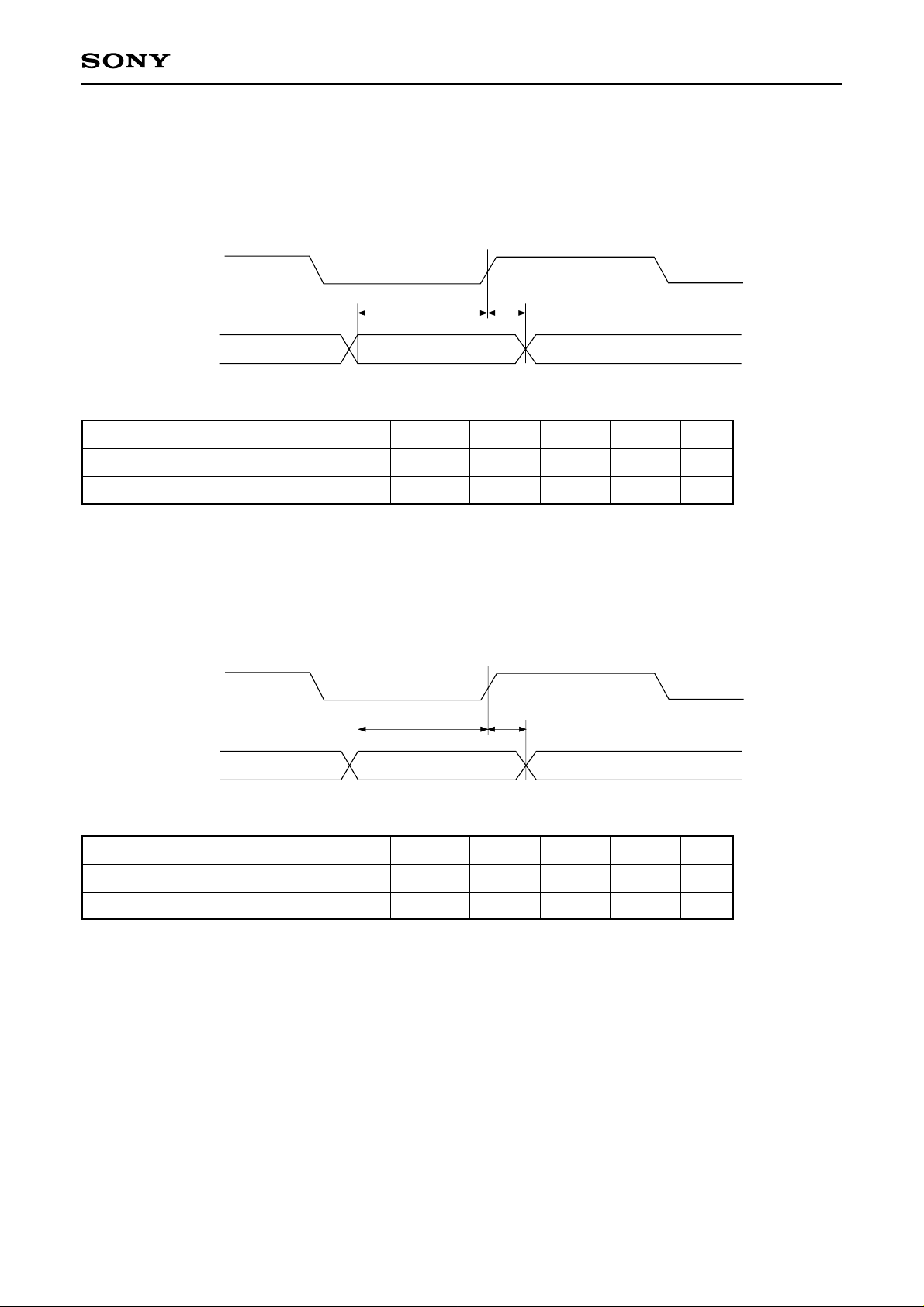
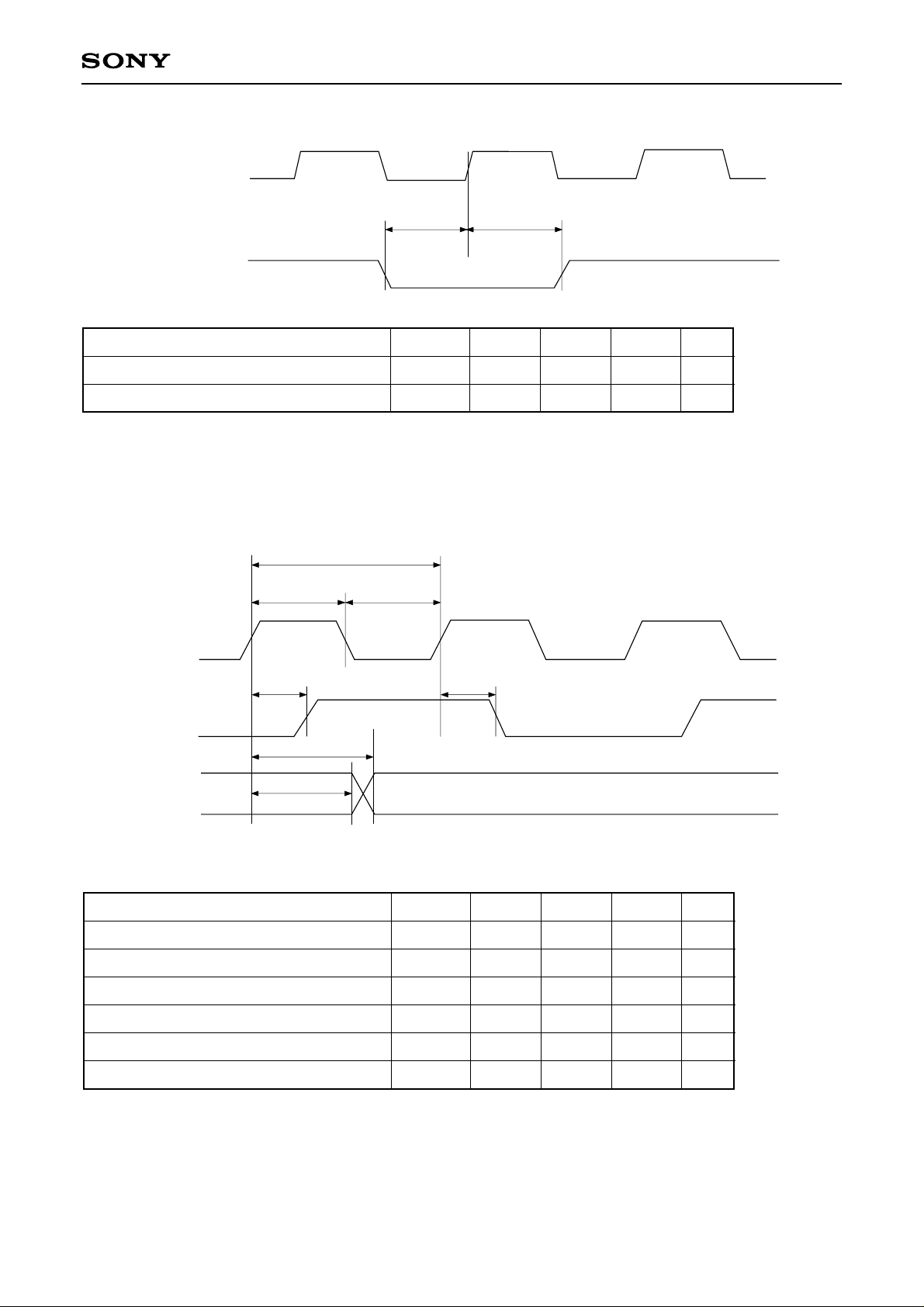
1. Pixel Data Interface
(1) 8-bit mode
SYSCLK
PD0 to 7
Item Symbol Min. Typ. Max. Unit
CXD1913AQ
tPDS tPDH
(Ta = 0 to +70°C, VDD = 3.3V ± 5%, 5.0V ±5%, Vss = 0V)
Pixel data setup time to SYSCLK
Pixel data hold time to SYSCLK
(2) 16-bit mode
PDCLK
PD0 to 15
Item Symbol Min. Typ. Max. Unit
Pixel data setup time to PDCLK
Pixel data hold time to PDCLK
tPDS
tPDH
tPDS tPDH
10
3
ns
ns
(Ta = 0 to +70°C, VDD = 3.3V ± 5%, 5.0V ± 5%, Vss = 0V)
tPDS
tPDH
20
0
ns
ns
– 8 –

2. Serial Port Interface
SCK
CXD1913AQ
fSCK
tPWLSCK tPWHSCK
tCSS
XCS
SI
SO
Item Symbol Min. Typ. Max. Unit
SCK clock rate
SCK pulse width Low
SCK pulse width High
Chip select setup time to SCK
Chip select hold time to SCK
Serial input setup time to SCK
tSIS tSIH
tSOD
tCSH
tSOH
(Ta = 0 to +70°C, VDD = 5.0V ± 5%, Vss = 0V)
fSCK
tPWLSCK
tPWHSCK
tCSS
tCSH
tSIS
DC
100
100
150
150
50
3
MHz
ns
ns
ns
ns
ns
Serial input hold time to SCK
Serial output delay time from SCK
Serial output hold time from SCK
Item Symbol Min. Typ. Max. Unit
SCK clock rate
SCK pulse width Low
SCK pulse width High
Chip select setup time to SCK
Chip select hold time to SCK
Serial input setup time to SCK
Serial input hold time to SCK
Serial output delay time from SCK
Serial output hold time from SCK
tSIH
∗
tSOD
∗
tSOH
(Ta = 0 to +70°C, VDD = 3.3V ± 5%, Vss = 0V)
fSCK
tPWLSCK
tPWHSCK
tCSS
tCSH
tSIS
tSIH
∗
tSOD
∗
tSOH
10
3
DC
100
100
150
150
50
10
3
30
∗
CL = 35pF
3
50
ns
ns
ns
MHz
ns
ns
ns
ns
ns
ns
ns
ns
– 9 –
∗
CL = 35pF
3. XVRST, F1
SYSCLK
CXD1913AQ
XVRST
F1
(Ta = 0 to +70°C, VDD = 3.3V ± 5%, 5.0V ± 5%, Vss = 0V)
Item Symbol Min. Typ. Max. Unit
XVRST setup time to SYSCLK
XVRST hold time to SYSCLK
4. SYSCLK, PDCLK, VSYNC, HSYNC, FID
fSYSCLK
tPWHCLK tPWLCLK
SYSCLK
tVS
tVH
tVS
20
0
tVH
ns
ns
tPDCLKD
PDCLK
tCOD
VSYNC,
HSYNC,
FID
tCOH
Item Symbol Min. Typ. Max. Unit
SYSCLK clock rate
SYSCLK pulse width Low
SYSCLK pulse width High
PDCLK delay time from SYSCLK
Control output delay time from SYSCLK
Control output hold time from SYSCLK
tPDCLKD
(Ta = 0 to +70°C, VDD = 5.0V ± 5%, Vss = 0V)
fSYSCLK
tPWLCLK
tPWHCLK
tPDCLKD
∗
tCOD
∗
tCOH
11
11
∗
3
27
15
20
∗
CL = 35pF
MHz
ns
ns
ns
ns
ns
– 10 –

(Ta = 0 to +70°C, VDD = 3.3V ± 5%, Vss = 0V)
Item Symbol Min. Typ. Max. Unit
CXD1913AQ
SYSCLK clock rate
SYSCLK pulse width Low
SYSCLK pulse width High
PDCLK delay time from SYSCLK
Control output delay time from SYSCLK
Control output hold time from SYSCLK
fSYSCLK
tPWLCLK
tPWHCLK
tPDCLKD
∗
tCOD
∗
tCOH
27
11
11
∗
3
23
25
MHz
ns
ns
ns
ns
ns
∗
CL = 35pF
– 11 –
 Loading...