

Sony CXD1812R, CXD1812Q Datasheet
ATAPI I/F CD-ROM DECODER
For the availability of this product, please contact the sales office.
CXD1812Q/R
Description
The CXD1812Q/R is a CD-ROM decoder LSI with
a built-in ATAPI I/F.
Features
• Compatible with CD-ROM, CD-I and CD-ROM XA
formats
• Real time error correction
• Automatic multi-block transfer function
• Readable Subcode-Q data by byte from the Sub
CPU
• Capable of transferring up to double speed
playback and Mode2 when the 33.8688 MHz clock
is used
Transfer in Mode3 is possible when the decoder is
OFF (The transfer speed depends on playback
speed and clock frequency.)
• Supports PIO/single-word DMA/multiword DMA
data transfer mode
• IORDY support available
• Automatic reception of PACKET commands
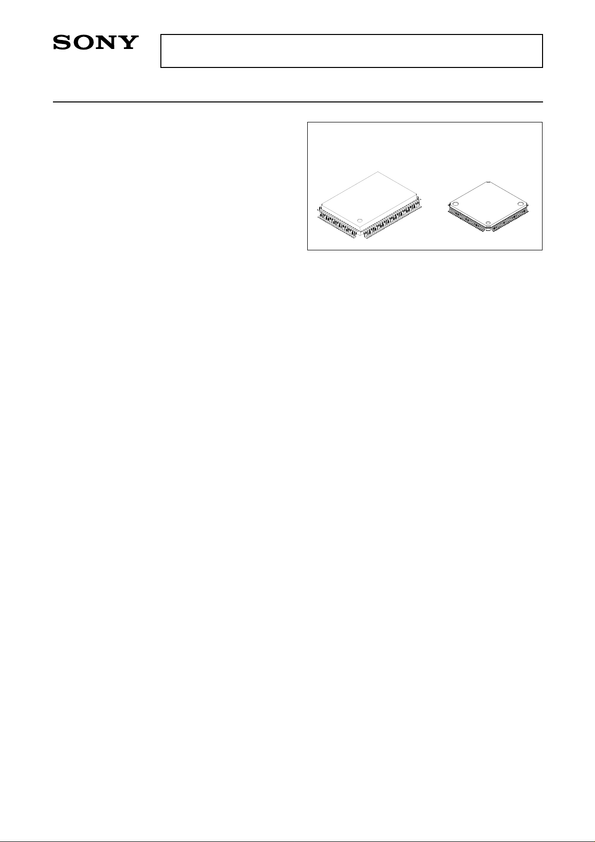
CXD1812Q
100 pin QFP (Plastic)
CXD1812R
100 pin LQFP (Plastic)
Absolute Maximum Ratings (Ta = 25°C)
• Supply voltage VDD –0.5 to +7.0 V
• Input voltage VI –0.5 to VDD +0.5 V
• Output voltage VO –0.5 to VDD +0.5 V
• Operating temperature Topr –20 to +75 °C
• Storage temperature Tstg –55 to +150 °C
Recommended Operating Conditions
• Supply voltage VDD 4.5 to 5.5 (+5.0 typ.) V
• Operating temperature Topr –20 to +75 °C
Applications
CD-ROM drives
Structure
Silicon gate CMOS IC
Sony reserves the right to change products and specifications without prior notice. This information does not convey any license by
any implication or otherwise under any patents or other right. Application circuits shown, if any, are typical examples illustrating the
operation of the devices. Sony cannot assume responsibility for any problems arising out of the use of these circuits.
– 1 –
E95233-ST
CXD1812Q/R
DD
V
XRST
MDB0 to 7
XMWR
XCAS
XRAS
HDB0 to F
69to72
95
3, 28, 53, 7843 to 46, 48 to 51
DMA FIFO
42
41
39
74to77
DMA
SEQUENCER
80to83
85to88
ATAPI REGISTERs
12 bytes PACKET FIFO
PRIORITY
RESOLVER
HCS0, 1
55
56
HA0 to 2
575860
XHRD
66
XHWR
67
HDRQ
XHAC
68
63
HOST I/F
HINT
62
XS16
61
REDY
64
XPDI
DASP
52
59
subCPU I/F
HRST
89
XINT
6
XWR
8
XRD
9
XCS
7
17 to 21, 23 to 25 10 to 14, 16
A0 to 5
D0 to 7
MA0 to 9
ADDRESS GEN
26, 27, 30 to 33, 35 to 38
4
1522293440475465737984
GND
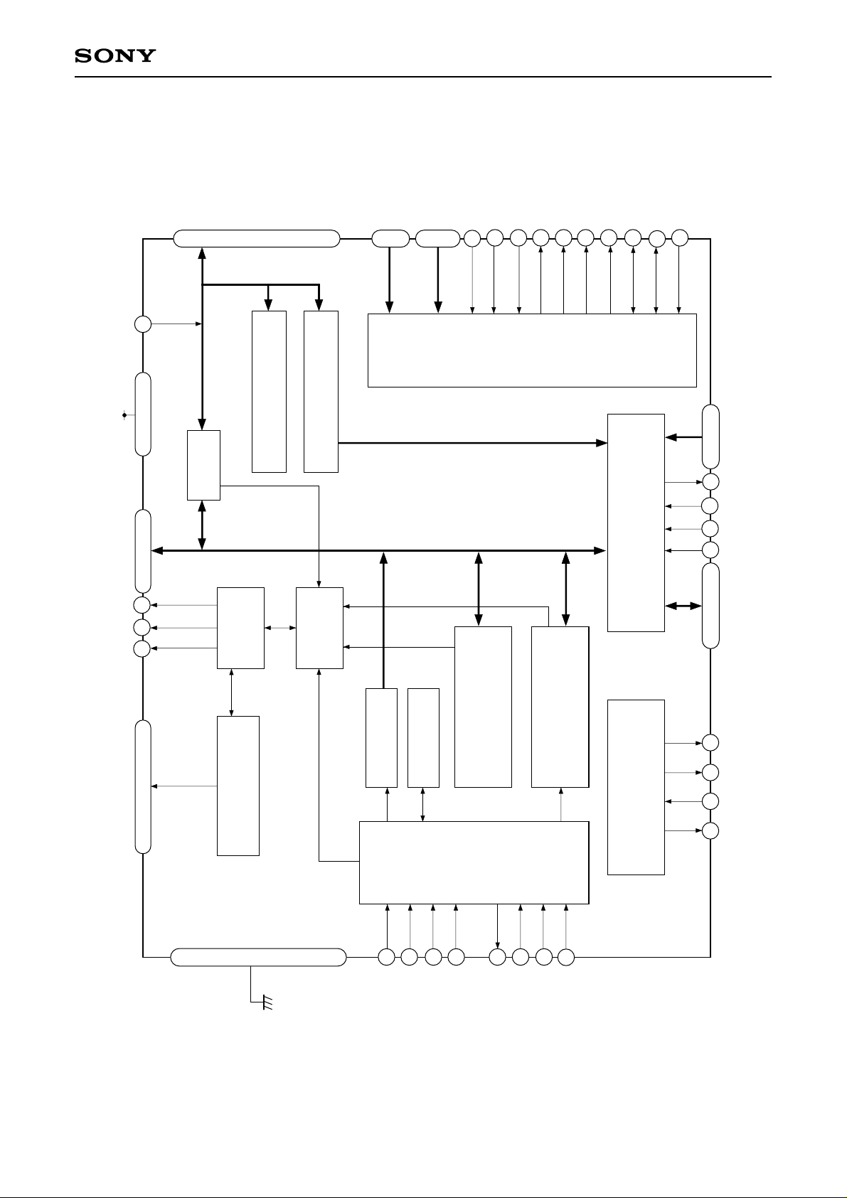
Block Diagram -1 CXD1812Q (QFP)
90
DESCRAMBLER
SYNC CONTROL
2
1
100
BCLK
C2PO
MDAT
– 2 –
MAIN DATA
ERROR CORECTION
I/F
CD•DSP
5
96
LRCK
EXCK
97
SBIN
Subcode S/P
98
99
SCOR
WFCK
93
94
92
CLOCK GENERATOR
91
MCLK
HCLK
XTL1
XTL2
CXD1812Q/R
DD
XRST
V
XMWR
XCAS
XRAS
MDB0 to 7
HDB0 to F
67to70
93
1, 26, 51, 76
DMA FIFO
41 to 44, 46 to 49
40
39
37
72to75
DMA
SEQUENCER
78to81
83to86
ATAPI REGISTERs
12 bytes PACKET FIFO
PRIORITY
RESOLVER
HCS0, 1
53
54
HA0 to 2
555658
XHRD
64
XHWR
65
HDRQ
XHAC
61
66
HOST I/F
HINT
60
XS16
59
REDY
62
XPDI
DASP
50
57
subCPU I/F
HRST
87
XINT
4
XWR
6
XRD
7
XCS
5
15 to 19, 21 to 23 8 to 12, 14
A0 to 5
D0 to 7
MA0 to 9
ADDRESS GEN
24, 25, 28 to 31, 33 to 36
2
1320273238455263717782
GND
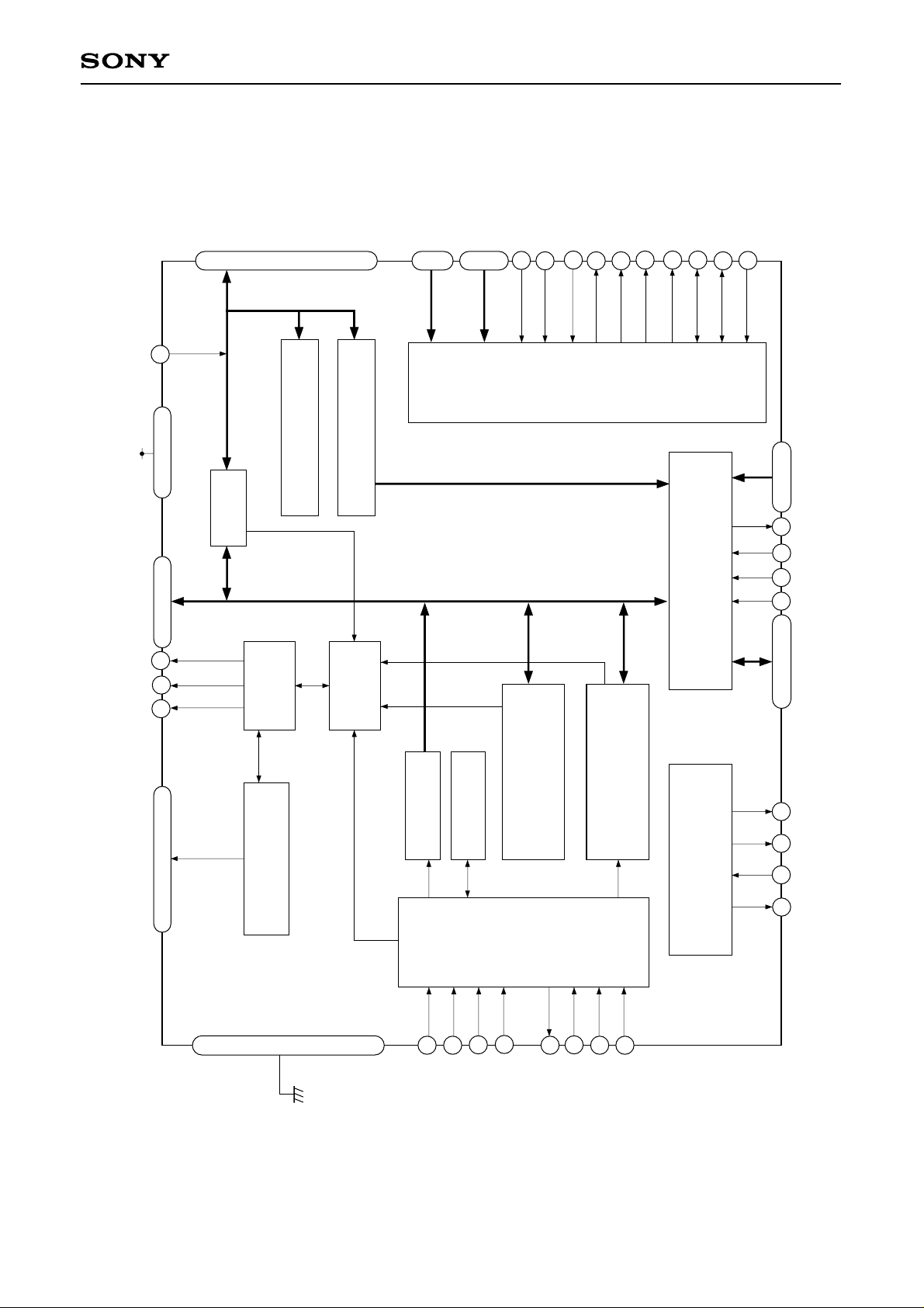
Block Diagram -2 CXD1812R (LQFP)
88
DESCRAMBLER
SYNC CONTROL
98
99
100
BCLK
C2PO
MDAT
– 3 –
MAIN DATA
ERROR CORECTION
I/F
CD•DSP
3
94
LRCK
EXCK
95
SBIN
Subcode S/P
96
97
SCOR
WFCK
91
92
90
CLOCK GENERATOR
89
MCLK
HCLK
XTL1
XTL2
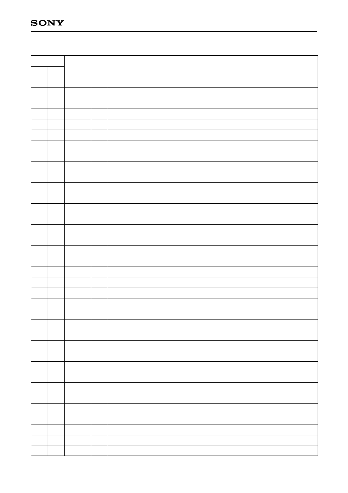
Pin Description
CXD1812Q/R
Pin No.
QFP
1
2
3
4
5
6
7
8
9
10
11
12
13
14
15
LQFP
99
100
1
2
3
4
5
6
7
8
9
10
11
12
13
Symbol
BCLK
MDAT
VDD
GND
LRCK
XINT
XCS
XWR
XRD
A5
A4
A3
A2
A1
GND
I/O Description
I
Bit clock signal from CD DSP
I
Data signal from CD DSP
—
Power supply
—
Ground
I
LR clock signal from CD DSP
O
Interrupt request signal to CPU
I
Chip select negative logic signal from CPU
I
Strobe negative logic signal for writing data from CPU
I
Strobe negative logic signal for reading data from CPU
I
CPU address (MSB)
I
CPU address
I
CPU address
I
CPU address
I
CPU address
—
Ground
16
17
18
19
20
21
22
23
24
25
26
27
28
29
30
31
32
14
15
16
17
18
19
20
21
22
23
24
25
26
27
28
29
30
A0
D7
D6
D5
D4
D3
GND
D2
D1
D0
MA0
MA1
VDD
GND
MA2
MA3
MA4
I
CPU address (LSB)
I/O
CPU data bus (MSB)
I/O
CPU data bus
I/O
CPU data bus
I/O
CPU data bus
I/O
CPU data bus
—
Ground
I/O
CPU data bus
I/O
CPU data bus
I/O
CPU data bus (LSB)
O
DRAM address (LSB)
O
DRAM address
—
Power supply
—
Ground
O
DRAM address
O
DRAM address
O
DRAM address
33
34
35
36
31
32
33
34
MA5
GND
MA6
MA7
O
DRAM address
—
Ground
O
DRAM address
O
DRAM address
– 4 –
CXD1812Q/R
Pin No.
QFP
37
38
39
40
41
42
43
44
45
46
47
48
49
50
51
LQFP
35
36
37
38
39
40
41
42
43
44
45
46
47
48
49
Symbol
MA8
MA9
XRAS
GND
XCAS
XMWR
MDB0
MDB1
MDB2
MDB3
GND
MDB4
MDB5
MDB6
MDB7
I/O Description
O
DRAM address
O
DRAM address (MSB)
O
DRAM row address strobe negative logic signal
—
Ground
O
DRAM column address strobe negative logic signal
O
DRAM write enable negative logic signal
I/O
DRAM data bus (LSB)
I/O
DRAM data bus
I/O
DRAM data bus
I/O
DRAM data bus
—
Ground
I/O
DRAM data bus
I/O
DRAM data bus
I/O
DRAM data bus
I/O
DRAM data bus (MSB)
52
53
54
55
56
57
58
59
60
61
62
63
64
65
66
67
68
50
51
52
53
54
55
56
57
58
59
60
61
62
63
64
65
66
DASP
VDD
GND
HCS1
HCS0
HA2
HA0
XPDI
HA1
XS16
HINT
XHAC
REDY
GND
XHRD
XHWR
HDRQ
I/O
Drive active/slave present negative logic signal; open drain output
—
Power supply
—
Ground
I
Chip select negative logic signal from host
I
Chip select negative logic signal from host
I
Host address (MSB)
I
Host address (LSB)
I/O
Passed diagnostics negative logic signal; open drain output
I
Host address
O
16-bit I/O port select negative logic signal; open drain output
O
Interrupt request positive logic signal to host
I
DMA acknowledge negative logic signal from host
O
I/O channel ready positive logic signal; open drain output
—
Ground
I
Strobe negative logic signal for reading data from host
I
Strobe negative logic signal for writing data from host
O
DMA request positive logic signal to host
69
70
71
72
67
68
69
70
HDBF
HDB0
HDBE
HDB1
I/O
Host data bus (MSB)
I/O
Host data bus (LSB)
I/O
Host data bus
I/O
Host data bus
– 5 –
CXD1812Q/R
Pin NO.
QFP
73
74
75
76
77
78
79
80
81
82
83
84
85
86
87
LQFP
71
72
73
74
75
76
77
78
79
80
81
82
83
84
85
Symbol
GND
HDBD
HDB2
HDBC
HDB3
VDD
GND
HDBB
HDB4
HDBA
HDB5
GND
HDB9
HDB6
HDB8
I/O Description
—
Ground
I/O
Host data bus
I/O
Host data bus
I/O
Host data bus
I/O
Host data bus
—
Power supply
—
Ground
I/O
Host data bus
I/O
Host data bus
I/O
Host data bus
I/O
Host data bus
—
Ground
I/O
Host data bus
I/O
Host data bus
I/O
Host data bus
88
89
90
91
92
93
94
95
96
97
98
99
100
86
87
88
89
90
91
92
93
94
95
96
97
98
HDB7
HRST
GND
XTL2
XTL1
MCLK
HCLK
XRST
EXCK
SBIN
SCOR
WFCK
C2PO
I/O
Host data bus
I
Chip reset negative logic signal from host
—
Ground
O
Crystal oscillation circuit output
I
Crystal oscillation circuit input
O
Master clock (XTL1) output
O
Clock output with 1/2 the frequency of XTL1
I
Chip reset negative logic signal
O
Subcode data read clock signal to CD DSP
I
Subcode data serial input signal from CD DSP
I
Subcode sync positive logic signal from CD DSP
I
Write frame clock signal from CD DSP
I
C2 pointer positive logic signal from CD DSP
– 6 –

CXD1812Q/R
Electrical Characteristics
1. DC Characteristics (VDD = 5V ±10%, VSS = 0V, Topr = –20 to +75°C)
Item Symbol Conditions Min. Typ. Max. Unit
High level input voltage (1)
Low level input voltage (1)
High level input voltage (2)
Low level input voltage (2)
High level input voltage (3)
Low level input voltage (3)
TTL Schmitt hysteresis
High level input voltage (4)
Low level input voltage (4)
CMOS Schmitt hysteresis
High level output voltage (6)
Low level output voltage (6)
High level output voltage (7)
Low level output voltage (7)
High level output voltage (8)
Low level output voltage (8)
Input leakage current
Input leakage current
∗1
VIH1
VIL1
VIH2
VIL2
Vt1+
Vt1–
Vt1+ – Vt1–
Vt2+
Vt2–
Vt2+ – Vt2–
VOH1
VOL1
VOH2
VOL2
VOH3
VOL3
IIL1
IIL2
IOH1 = –2mA
IOL1 = 4mA
IOH2 = –6mA
IOL2 = 12mA
IOH3 = –6mA
IOL3 = 4mA
2.2
0.7VDD
2.2
0.8VDD
VDD – 0.8
VDD – 0.8
VDD – 0.8
–10
–40
0.4
0.6
0.8
0.3VDD
0.8
0.2VDD
0.4
0.4
0.4
10
40
V
V
V
V
V
V
V
V
V
V
V
V
V
V
V
V
µA
µA
Input current of pull-up input
Input current of pull-up input
∗1
Output leakage current (9) (10)
Oscillation cell logic threshold value
Oscillation cell high level input voltage
Oscillation cell low level input voltage
Oscillation cell feedback resistance
Oscillation cell high level output voltage
Oscillation cell low level output voltage
∗1
Bidirectional pin
IIL3
IIL4
IIZ
LVth
VIH
VIL
RFB
VOH
VOL
VIN = 0V
VIN = 0V
High-impedance state
VIN = VSS or VDD
IOH = –12mA
IOL = 12mA
–40
–90
–40
0.7VDD
250k
0.5VDD
–100
–200
0.5VDD
1M
–240
–440
40
0.3VDD
2.5M
0.5VDD
µA
µA
µA
V
V
V
Ω
V
V
– 7 –

1-1. Categories of input pins
(1) TTL input level pin:
D0 to D7, MDB0 to MDB7, HDB0 to HDBF, DASP, XPDI
(2) CMOS input level pin:
MDAT, LRCK, SBIN, SCOR, WFCK, C2PO
(3) TTL Schmitt input level pin:
XCS, XWR, XRD, A0 to A5, HA0 to HA2, XHAC, XHRD, XHWR, HCS0 to HCS1, HRST
(4) CMOS Schmitt input level pin:
BCLK, XRST
(5) Input pin with pull-up resistor:
D0 to D7, MDB0 to MDB7, HCS0 to HCS1, HRST
1-2. Categories of output pins
(6) Normal output pin:
D0 to D7, MDB0 to MDB7, XINT, MA0 to MA9, XMWR, MCLK, HCLK, EXCK
(7) Powered output pin:
HINT, HDRQ, HDB0 to HDBF, DASP, XPDI, XS16, REDY
(8) Proportional output pin:
XRAS, XCAS
(9) Tristate output pin:
XINT, HINT, HDRQ
(10) Open drain output pin:
DASP, XPDI, XS16, REDY
CXD1812Q/R
1-3. Bidirectional pins
D0 to D7, MDB0 to MDB7, HDB0 to HDBF, DASP, XPDI
1-4. Oscillation cell
Input: XTL1
Output: XTL2
1-5. I/O Capacitance (VDD = VI = 0V, f = 1MHz)
Item Symbol Min. Typ. Max. Unit
Input capacitance
Output capacitance
I/O capacitance
CIN
COUT
CI/O
9
11
11
pF
pF
pF
– 8 –

2. AC Characteristics (VDD = 5V ±10%, VSS = 0V, Topr = –20 to +75°C, Output Load = 50pF)
2-1. CPU Interface
(1) Read
A0 to A5
XCS
Trdw
CXD1812Q/R
(2) Write
XRD
D0 to D7
A0 to A5
XCS
XWR
D0 to D7
Tas
Tas
Tdd
Twwr
Tds
Tah
Tdf
Tah
Tdh
Item Symbol Min. Typ. Max. Unit
Address setup time (for XCS & XRD/XWR ↓)
Address hold time (for XCS & XRD/XWR ↑)
XRD pulse width
Data delay time (for XCS & XRD ↓)
Data float time (for XCS & XRD ↑)
XWR pulse width
Address setup time (for XCS & XWR ↑)
Address hold time (for XCS & XWR ↑)
– 9 –
Tas
Tah
Trdw
Tdd
Tdf
Twwr
Tds
Tdh
43
21
0
0
ns
ns
ns
43
1
ns
ns
ns
7
0
ns
ns
2-2. DRAM Interface
(1) Read
XRAS
XCAS
Tasr
CXD1812Q/R
Tras Trp
Trcd Tcas Tpc
Tasc
(2) Write
MA0 to MA9
MDB0 to 7
XMWR
XRAS
XCAS
MA0 to MA9
MDB0 to 7
XMWR
Tasr
row
Trah
row
Trah
col
Trcd Tcas Tpc
col
Tids Tidh
col
Tcah
high
Tras Trp
Tasc
col
Tdos Tdof
col
Tcah
rowcol
row
Item Symbol Min. Typ. Max. Unit
RAS pulse width
RAS precharge width
RAS – CAS delay time
CAS pulse width
Page mode cycle time
Row address setup time (for RAS ↓)
Row address hold time (for RAS ↓)
Column address setup time (for CAS ↓)
Column address hold time (for CAS ↓)
Input data setup time (for CAS ↑)
Input data hold time (for CAS ↑)
Data output setup time (for CAS ↓)
Data output float time (for CAS ↓)
– 10 –
Tras
Trp
Trcd
Tcas
Tpc
Tasr
Trah
Tasc
Tcah
Tids
Tidh
Tdos
Tdof
3Tw
Tw – 7
Tw
Tw – 14
Tw + 2
7
0
0
Tw + 3
2Tw
2Tw
Tw
2Tw
(Tw = 1/f)
ns
ns
ns
ns
ns
ns
ns
ns
ns
ns
ns
ns
ns
2-3. HOST Interface
(1) PIO
HCS0, 1
HA0 to 2
XS16
CXD1812Q/R
Txsl
Trww
XHRD
XHWR
HDB0 to F
REDY
Tas
Tdd
Trel Trel
Item Symbol Min. Typ. Max. Unit
Address setup time (for XHRD/XHWR ↓)
Address hold time (for XHRD/XHWR ↑)
XHRD/XHWR pulse width
Data delay time (for XHRD ↓)
Data float time (for XHRD ↑)
Data setup time (for XHWR ↑)
Tah Tas Trww Tah
Tdf
Tas
Tah
Trww
Tds Tdh
20
5
50
Tdd
Tdf
Tds
5
20
26
21
ns
ns
ns
ns
ns
ns
Data hold time (for XHWR ↑)
XS16 fall time (for Address valid)
REDY fall time (for XHRD/XHWR ↓)
– 11 –
Tdh
Txsl
Trel
5
8
14
ns
ns
ns

(2) Single-word DMA
CXD1812Q/R
HDRQ
XHAC
XHRD/
XHWR
HDB0 to F
(READ)
HDB0 to F
(WRITE)
(3) Multiword DMA
HDRQ
XHAC
Trql
Tacs Trww Tach
Tdd
Tdf
TdhTds
Trql
TachTrwwThpwTrwwTacs
XHRD/
XHWR
Tdd
HDB0 to F
(READ)
HDB0 to F
(WRITE)
Item Symbol Min. Typ. Max. Unit
HDRQ fall time (for XHAC/XHRD/XHWR ↓)
XHRD/XHWR Low pulse width
Data delay time (for XHRD ↓)
Data float time (for XHRD ↑)
Data setup time (for XHWR ↑)
Data hold time (for XHWR ↑)
XHAC setup time (for XHRD/XHWR ↓)
Tdf
Tdd Tdf
TdhTds
Tds Tdh
(Tw = 1/f)
Trql
Trww
Tdd
Tdf
Tds
Tdh
Tacs
50
5
20
5
0
Tw +11
26
19
ns
ns
ns
ns
ns
ns
ns
XHAC hold time (for XHRD/XHWR ↑)
XHRD/XHWR high pulse width
– 12 –
Tach
Thpw
0
25
ns
ns

2-4. CD DSP Interface
(1) BCKRED = "H"
BCLK
MDAT
LRCK
C2PO
(2) BCKRED = "L"
CXD1812Q/R
Tbck Tbck
Tsb1 Thb1
Tsb2 Thb2
BCLK
MDAT
LRCK
C2PO
Item Symbol Min. Typ. Max. Unit
BCLK frequency
BCLK pulse width
MDAT setup time (for BCLK)
MDAT hold time (for BCLK)
LRCK, C2PO setup time (for BCLK)
Tbck Tbck
Tsb1 Thb1
Tsb2 Thb2
Fbck
Tbck
Tsb1
Thb1
Tsb2
25
12
12
12
20 MHz
ns
ns
ns
ns
LRCK, C2PO hold time (for BCLK)
– 13 –
Thb2
12
ns
2-5. Subcode Interface
CXD1812Q/R
Subcode Frame
WFCK
SCOR
SBIN
EXCK
EXCK
SF97 SF0 SF1 SF2 SF3
Twed
Teck Teck
SBIN
Item Symbol Min. Typ. Max. Unit
WFCK – EXCK delay time
EXCK pulse width
SBIN setup time (for EXCK ↑)
SBIN hold time (for EXCK ↑)
a = 48: When EXCKSL (CONFIG0 register bit 3) = High
a = 32: When EXCKSL (CONFIG0 register bit 3) = Low
Tds Tdh
Twed
Teck
Tds
Tdh
2aTw
1/2aTw – 2
12
12
(Tw = 1/f)
3aTw ns
ns
ns
ns
– 14 –
CXD1812Q/R
2-6. XTL1 and XTL2 Pins
(1) When using self-excited oscillation
Item Symbol Min. Typ. Max. Unit
Oscillation frequency f 33.8688 40 MHz
(2) When inputting a pulse to the XTL1 pin
Tw
Twhx Twlx
Vihx
DD/2
V
High level pulse width
Low level pulse width
Pulse cycle
Vilx
Item Symbol Min. Typ. Max. Unit
Twhx
Twlx
Tw
10
10
29
ns
ns
ns
– 15 –

CXD1812Q/R
Description of Functions
1. Pin Description
The pin description by function is given below.
1-1. CD player interface (8 pins)
This enables direct connection with the Sony's digital signal processor LSI for CD players. Digital signal
processor LSI for CD applications are hereafter called "CD DSP."
(1) MDAT (medium data: input)
Serial data stream from CD DSP.
(2) BCLK (bit clock: input)
Bit clock signal; MDAT signal strobe.
(3) LRCK (LR clock: input)
LR clock signal; indicates left and right channels of MDAT signals.
(4) C2PO (C2 pointer: input)
C2 pointer signal; indicates that an error is contained in MDAT input.
(5) WFCK (write frame clock: input)
Write frame clock input signal.
(6) SCOR (subcode sync OR: input)
Subcode sync signal.
(7) SBIN (subcode serial input: input)
Subcode serial signal.
(8) EXCK (external clock: output)
Clock output for reading SBIN signals.
1-2. Buffer memory interface (21 pins)
This can be connected with up to a 512K-byte DRAM (4M bits).
(1) XMWR (DRAM write enable: output)
DRAM write enable negative logic output signal.
(2) XCAS (column address strobe: output)
Negative logic output signal to indicate that column addresses are valid.
(3) XRAS (row address strobe: output)
Negative logic output signal to indicate that row addresses are valid.
(4) MA0 to MA9 (DRAM address: output)
DRAM address output.
(5) MDB0 to MDB7 (DRAM data bus: input/output)
DRAM data bus signal; pulled up by a standard 25kΩ resistor.
1-3. Sub CPU interface (18 pins)
(1) XWR (sub CPU write: input)
Strobe negative logic signal for writing internal registers.
(2) XRD (sub CPU read: input)
Strobe negative logic signal for reading internal registers status.
(3) D0 to D7 (sub CPU data bus: input/output)
8-bit data bus; pulled up by a standard 25kΩ resistor.
(4) A0 to A5 (sub CPU address: input)
Address signal for selecting internal registers from sub CPU.
(5) XINT (sub CPU interrupt: output)
Interrupt request signal to sub CPU. Polarity can be controlled by sub CPU.
(6) XCS (chip select: input)
Chip select negative logic signal from sub CPU.
– 16 –

1-4. HOST interface (31 pins)
(1) HCS0 (host chip select: input)
Chip select negative logic signal from host; pulled up by a standard 50kΩ resistor. This is connected with
the CS1FX pin of ATAPI I/F.
(2) HCS1 (host chip select: input)
Chip select negative logic signal from host; pulled up by a standard 50kΩ resistor. This is connected with
the CS3FX pin of ATAPI I/F.
(3) HA0 to HA2 (host address: input)
Address signal for selecting internal registers from host.
(4) DASP (drive active/slave present: input/output)
Negative logic signal to indicate that slave drive is present or drive is active; open drain signal.
(5) HDB0 to HDBF (host data bus: input/output)
16-bit host data bus signal.
(6) XHRD (host read: input)
Data read strobe negative logic signal from host.
(7) XHWR (host write: input)
Data write strobe negative logic signal from host.
(8) XHAC (host DMA acknowledge: input)
DMA data request acknowledge negative logic signal from host.
(9) HDRQ (host DMA request: output)
DMA data request positive logic signal to host; tristate output.
(10) HINT (host interrupt: output)
Interrupt request positive logic signal to host; tristate output.
(11) XS16 (16-bit data transfer: output)
Negative logic signal to indicate that the 16-bit data port has been selected; open drain signal. This is
connected with the IOCS16 pin of ATAPI I/F.
(12) REDY (I/O channel ready: output)
Positive logic signal to be negated when the drive is not ready to respond to a data transfer reguest; open
drain signal. This is connected with the IORDY pin of ATAPI I/F.
(13) XPDI (passed diagnostics: input/output)
Negative logic signal that indicates diagnostics of the slave drive has been completed; open drain signal.
This is connected with the PDIAG pin of ATAPI I/F.
(14) HRST (host reset: input)
Reset negative logic signal from host; pulled up by a standard 50kΩ resistor.
CXD1812Q/R
1-5. Others (5 pins)
(1) XRST (reset: input)
Chip reset negative logic input signal.
(2) XTL1 (crystal 1: input)
(3) XTL2 (crystal 2: output)
A crystal oscillator is connected between XTL1 and XTL2. (The capacitor value depends on the crystal
oscillator.)
(4) MCLK (clock: output)
Outputs a clock signal of the same frequency as that of XTL1. The output can be set at low when this
clock signal is not used.
(5) HCLK (half clock: output)
Outputs a clock signal with 1/2 the frequency of XTL1. The output can be set at low when this signal is
not used.
1-6. Power supply (17 pins)
VDD: 4 pins, GND: 13 pins.
– 17 –
 Loading...