

Sony CXD1807Q Datasheet

CD-G Decoder
For the availability of this product, please contact the sales office.
Description
The CXD1807Q has functions to decode CD-G
commands written in the CD subcode and write
them into the DRAM to display them. It also has a
built-in RGB 4-bit D/A converter. By adding 256K
bits of DRAM and a video encoder, a CD graphics
system can be configured.
Functions
• Real-time correction of subcode errors
• Powerful protection circuit for subcode synchronization
• RAM for color look-up table
• Compatible with both NTSC and PAL
• 4-bit DAC for RGB
• 80-pin QFP
CXD1807Q
80 pin QFP (Plastic)
Applications
CD-G decoder
Structure
Silicon gate CMOS IC
Absolute Maximum Ratings (Ta = 25°C)
• Supply voltage VDD VSS–0.5 to +7.0 V
• Input voltage VI VSS–0.5 to VDD +0.5 V
• Output voltage VO VSS–0.5 to VDD +0.5 V
• Operating temperature Topr –20 to +75 °C
• Storage temperature Tstg –55 to +150 °C
Recommended Operating Conditions
• Supply voltage DVDD 5±0.5 V
AVDD 5±0.5 V
• Ambient temperature Ta –20 to +75 °C
Sony reserves the right to change products and specifications without prior notice. This information does not convey any license by
any implication or otherwise under any patents or other right. Application circuits shown, if any, are typical examples illustrating the
operation of the devices. Sony cannot assume responsibility for any problems arising out of the use of these circuits.
– 1 –
E94643-ST
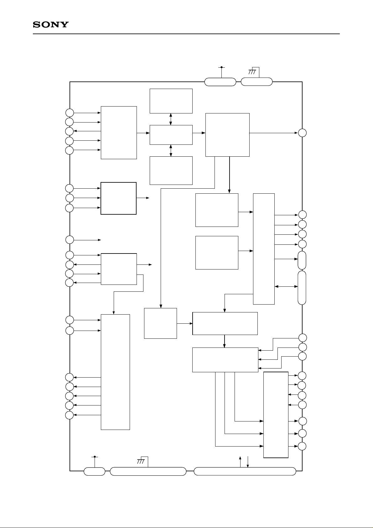
Block Diagram
CXD1807Q
SCOR
WFCK
EXCK
SBSO
MUTE
CLK
DIN
XLT
XRST
XIN
XOUT
XTL1
XTL2
20
19
35
36
37
38
34
26
27
28
18
17
24
SUB CODE
Interface
CPU Interface
CK
Gen.
Buffer RAM
Buffer RAM
Manager
Error Correction
68, 72, 76
AVDD
CD-G
Instruction
Decode
VRAM
Graphics Control
Display Address
Generation
70, 74, 78
AVSS
DRAM
R/W
Control
CDG
39
46
OE1
47
WE1
RAS1
48
CAS1
49
55
A10 to A17
to
62
50
51
D10 to D13
53
54
INTR
NTSC
FSC1
CBLK
VSYC
HSYC
CSYC
15
16
80
CLUT RAM
Control
SYNC
Gen.
1
3
4
5
8, 33
DVDD DVSS
2, 7, 12, 23, 32, 42, 52, 63
CLUT RAM
RGB
Output Control
R0 to R3
G0 to G3
B0 to B3
6, 9 to 11, 13, 14, 29 to 31, 40, 41, 43 to 45
TST0 to TSTD
D/A
21
25
75
66
67
77
22
71
69
73
CBAR
APCJ
VOFF
VB
IRF
VRF
VG
ROUT
GOUT
BOUT
– 2 –

Pin Description
CXD1807Q
Pin
No.
1
2
3
4
5
6
7
8
9
10
11
12
13
14
15
Symbol I/O Description
CBLK
DVSS
VSYC
HSYC
CSYC
TST8
DVSS
DVDD
TST9
TST4
TST5
DVSS
TST6
TST7
INTR
O
—
O
O
O
O
—
—
O
—
Composite blanking signal; negative logic
Digital ground
Vertical sync signal; negative logic
Horizontal sync signal; negative logic
Composite sync signal; negative logic
Test pin
Digital ground
Digital power supply
Test pin
I
Test pin
I
Test pin
Digital ground
I
Test pin
I
Test pin
I
Interlace/non-interlace (High/Low) switching signal
16
17
18
19
20
21
22
23
24
25
26
27
28
29
30
31
32
NTSC
XOUT
XIN
XTL2
XTL1
CBAR
APCJ
DVSS
XRST
VOFF
CLK
DIN
XLT
TSTA
TSTB
TSTC
DVSS
O
O
—
O
O
O
—
I
NTSC/PAL (High/Low) select signal
14.31818MHz (NTSC 4fsc) crystal oscillator circuit output
I
14.31818MHz (NTSC 4fsc) crystal oscillator circuit input
17.734475MHz (PAL 4fsc) crystal oscillator circuit output
I
17.734475MHz (PAL 4fsc) crystal oscillator circuit input
I
Color bar output select signal; positive logic
I
APC-adjusting input signal; positive logic
Digital ground
I
Reset input signal; negative logic
I
R, G, B output mute select signal; positive logic
I
Data write clock signal from CPU
I
Serial data input signal from CPU
I
Data latch signal from CPU
Test pin
Test pin
Test pin
Digital ground
33
34
DVDD
MUTE
—
Digital power supply
I
Subcode data mute signal; positive logic
– 3 –
CXD1807Q
Pin
No.
35
36
37
38
39
40
41
42
43
44
45
46
47
48
49
Symbol I/O Description
SCOR
WFCK
EXCK
SBSO
CDG
TSTD
TST3
DVSS
TST2
TST1
TST0
OE1
WE1
RAS1
CAS1
O
O
O
—
O
O
O
O
I
Subcode sync signal from CD DSP; positive logic
I
Write frame clock signal from CD DSP
Subcode data readout clock signal to CD DSP
I
Subcode data P to W serial input signal from CD DSP
Disc identification signal
Test pin
I
Test pin
Digital ground
I
Test pin
I
Test pin
I
Test pin
DRAM output enable signal; negative logic
DRAM write enable signal; negative logic
DRAM row address strobe signal; negative logic
DRAM column address strobe signal; negative logic
50
51
52
53
54
55
56
57
58
59
60
61
62
63
64
65
66
D10
D11
DVSS
D12
D13
A10
A11
A12
A13
A14
A15
A16
A17
DVSS
N.C.
N.C.
IRF
I/O
I/O
—
I/O
I/O
O
O
O
O
O
O
O
O
—
—
—
O
DRAM data bus (LSB)
DRAM data bus
Digital ground
DRAM data bus
DRAM data bus (MSB)
DRAM address (LSB)
DRAM address
DRAM address
DRAM address
DRAM address
DRAM address
DRAM address
DRAM address (MSB)
Digital ground
Connect a resistance 15 times the output resistance.
67
68
69
70
71
VRF
AVDD1
ROUT
AVSS1
VG
—
O
—
I
Sets the full-scale value of RGB output signal.
Analog power supply for R channel/DA converter
Analog red signal output
Analog ground for R channel/DA converter
I
Connect a power supply through an approximately 0.1µF capacitor.
– 4 –
CXD1807Q
Pin
No.
72
73
74
75
76
77
78
79
80
Sumbol I/O Description
AVDD2
GOUT
AVSS2
VB
AVDD3
BOUT
AVSS3
N.C.
FSC1
—
O
—
O
—
O
—
—
O
Analog power supply for G channel/DA converter
Analog green signal output
Analog ground for G channel/DA converter
Connect GND through an approximately 0.1µF capacitor.
Analog power supply for B channel/DA converter
Analog blue signal output
Analog ground for B channel/DA converter
3.58MHz (NTSC), 4.43MHz (PAL) clock output (sub carrier clock signal)
– 5 –
CXD1807Q
Electrical Characteristics
1. DC Characteristics (VDD = 5V±10%, VSS = 0V, Topr = –20 to +75°C)
Item Symbol Conditions Min. Typ. Max. Unit
Supply current
High level input voltage (1)
Low level input voltage (1)
High level input voltage (2)
Low level input voltage (2)
High level input voltage (3)
Low level input voltage (3)
TTL Schmitt hysteresis
High level input voltage (4)
Low level input voltage (4)
CMOS Schmitt hysteresis
Input current of pull-up input (5)
High level output voltage (6)
Low level output voltage (6)
High level output voltage (7)
Low level output voltage (7)
High level output voltage (8)
IDD
VIH1
VIL1
VIH2
VIL2
Vt1 +
Vt1 –
Vt1 + – Vt1 –
Vt2 +
Vt2 –
Vt2 + – Vt2 –
IIN
VOH1
VOL1
VOH2
VOL2
VOH3
Operating state
VIN = 0V
IOH1 = –2mA
IOL1 = 4mA
IOH1 = –4mA
IOL1 = 8mA
IOH1 = –6mA
2.2
0.7VDD
2.2
0.8VDD
–40
VDD–0.8
VDD–0.8
VDD–0.8
0.4
0.6
–100
100
0.8
0.3VDD
0.8
0.2VDD
–240
0.4
0.4
mA
V
V
V
V
V
V
V
V
V
V
µA
V
V
V
V
V
Low level output voltage (8)
Input leak current
Oscillation cell logic threshold
Oscillation cell high level input
voltage
Oscillation cell low level input
voltage
Oscillation cell feedback
resistance
Oscillation cell high level output
voltage
Oscillation cell low level output
voltage
1-1. Classification of input pins
(1) TTL level input:
DIN, XLT, D10 to D13
(2) CMOS level input:
INTR, NTSC, SCOR, SBSO, MUTE, APCJ, VOFF, CBAR, TST0 to TST7
(3) TTL Schmitt input:
CLK
(4) CMOS Schmitt input:
XRST, WFCK
(5) Pull-up input:
D10 to D13
VOL3
IIL1
LVth
VIH
VIL
RFB
VOH
VOL
IOL1 = 4mA
VIN = VSS or VDD
IOH = –3mA
IOL = 3mA
– 6 –
–10
0.7VDD
250k
0.5VDD
0.5VDD
1M
0.4
10
0.3VDD
2.5M
0.5VDD
V
µA
V
V
V
Ω
V
V
 Loading...