

Sony CXD1804BR Datasheet

– 1 –
CXD1804BR
E96X34A73
CD-ROM Decoder
Description
The CXD1804BR is a CD-ROM decoder LSI with a
built-in Fast SCSI controller.
Features
• Fast SCSI controller (Target mode)
• Maximum transfer speed of 10MB/s (when using
Fast SCSI synchronous transfer)
• SCSI overhead reduced by executing multiple
SCSI sequences
• Supports SCAM Level 2
• Compatible with CD-ROM, CD-I and CD-ROM XA
formats
• Real-time error correction
• Capable of handling up to 20 x speed playback
• Multiblock auto-transfer function
• Can read subcode-Q data for each byte from the
sub CPU
• Real-time subcode (R to W) error correction
• Serial transfer of commands to CD DSP
• Connectable with standard DRAM of up to 8M bits
(1024K bytes)
• DRAM bit width selectable for 8 bits or 16 bits
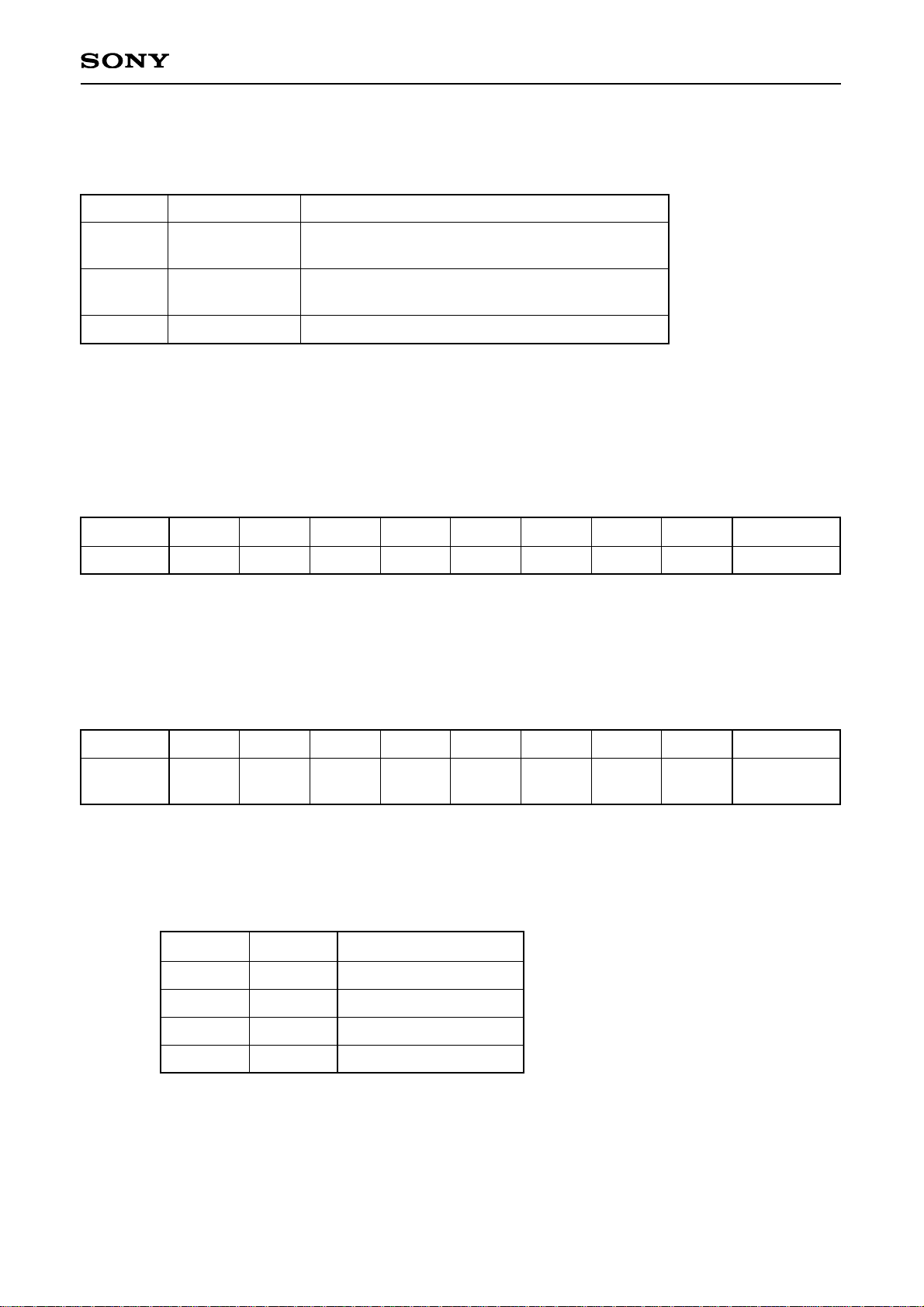
Absolute Maximum Ratings (Ta = 25°C)
• Supply voltage VDD –0.5 to +7.0 V
• Input voltage VI –0.5 to VDD + 0.5 V
• Output voltage VO –0.5 to VDD + 0.5 V
• Operating temperature Topr –20 to +75 °C
• Storage temperature Tstg –55 to +150 °C
Recommended Operating Conditions
• Supply voltage VDD 4.5 to 5.5 (5.0 typ.) V
• Operating temperature Topr –20 to +75 °C
Applications
CD-ROM drives
Structure
Silicon gate CMOS IC
Sony reserves the right to change products and specifications without prior notice. This information does not convey any license by
any implication or otherwise under any patents or other right. Application circuits shown, if any, are typical examples illustrating the
operation of the devices. Sony cannot assume responsibility for any problems arising out of the use of these circuits.
144 pin LQFP (Plastic)
For the availability of this product, please contact the sales office.
– 2 –
CXD1804BR
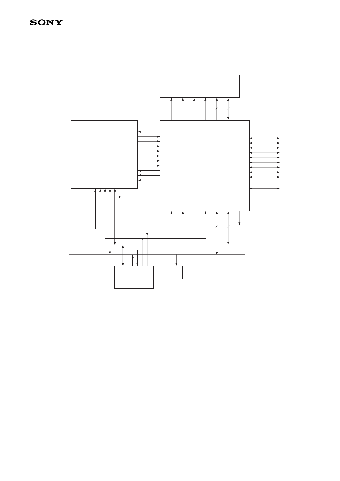
Connection Example
Address
Decoder
sub CPU
CPU data bus
CPU address bus
8bit7bit
16bit10bit
SCSI Bus
XATN
XBSY
XACK
XRST
XSEL
XMSG
XCD
XREQ
XIO
XDBP, XDB (7:0)
EXCK
SBIN
SCOR
WFCK
C2PO
BCLK
MDAT
LRCK
XLAT
DATO
DSTB
A (6:0)XCS
XWR
XWAT
XRD D (7:0)
INT
MDB
(15:0)
MA
(9:0)
XRAS
XLCAS
XUCAS
XMWR
CXD1804AR
CD-ROM Decoder
&
SCSI I/F
CD DSP
Buffer RAM
– 3 –
CXD1804BR
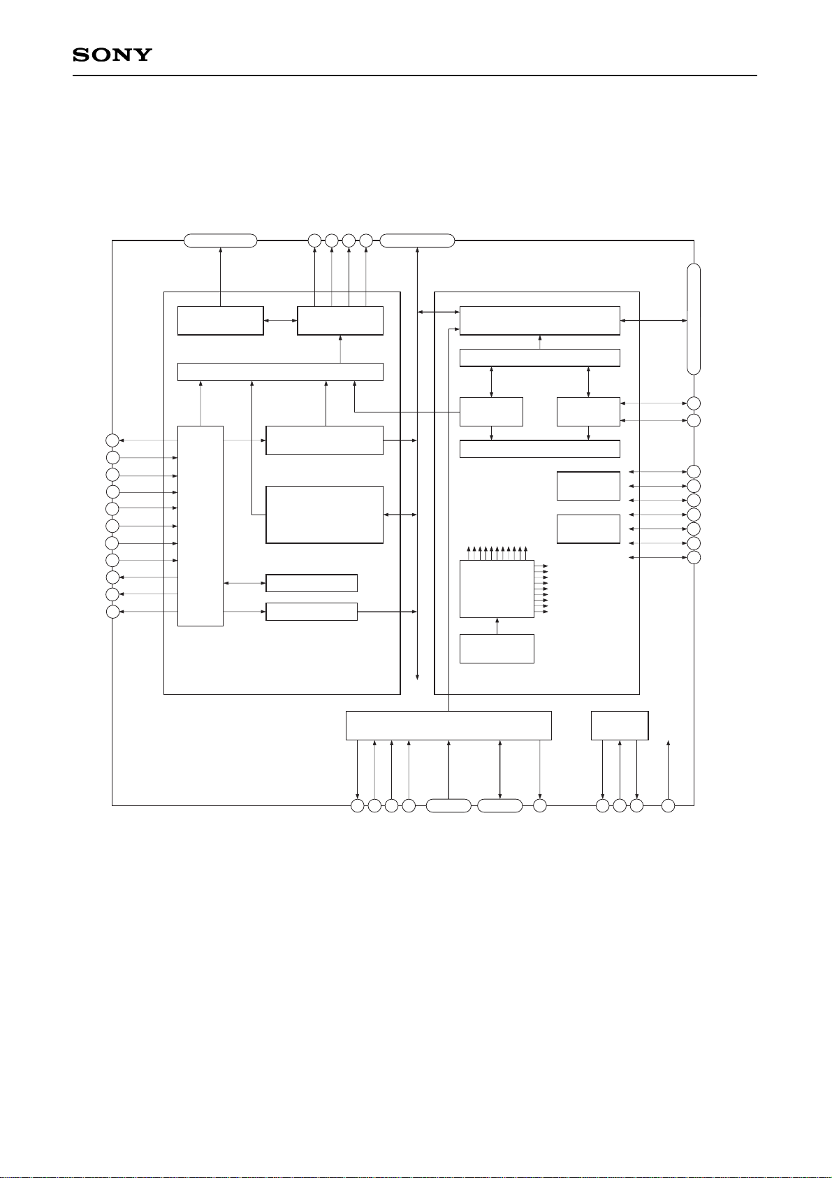
Block Diagram
47
39
43
40
26
28
32
31
45
65
64
63
62
119
120
121
50
141
142
143
144
122
123 to 129 131 to 138
51 to 57, 59 to 61
68 to 75, 77 to 84
3
•
5
•
8
•
10
•
11
•
15
•
18
•
20
•
23
CD-ROM Decoder Block SCSI Controller Block
sub CPU
I/F
Descrambler
Sync Control
Priority Resolver
FIFO Control
16byte FIFO
24bit Transfer Byte Counter
Clock
Gen.
Microcode
ROM
Microcode
Core
&
Registers
Arbitration
Selection
SCSI
Phase Ctrl
SCSI
Handshake
Buffer
Handshake
Buffer
Address Gen.
DMA
Sequencer
Subcode
Deinterleave & ECC
Main Data
Error Correction
MA (0:9) MDB (0:15)XMWRXUCAS
XLCASXCAS
EXCK
SBIN
SCOR
WFCK
C2PO
BCLK
MDAT
LRCK
DATO
XLAT
DSTB
XDB (0:7)
XDBP
XREQ
XACK
XRST
XBSY
XATN
XSEL
XCD
XMSG
XIO
D (7:0)A (0:6) XWAT XTL2 CLK
XTL1
XRESXCS
XWRINT
XRD
87
88
89
90
91
92
93
94
98
99
100
CD DSP
I/F
– 4 –
CXD1804BR
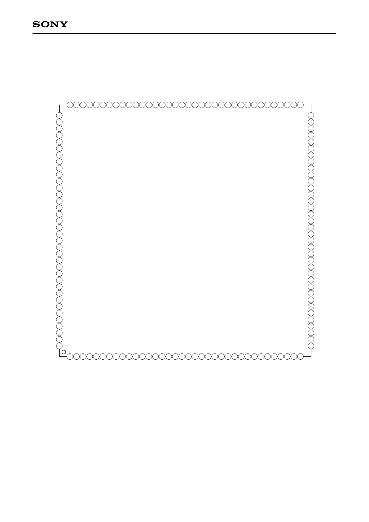
Pin Configuration
36
35
34
31
32
33
2
3
4
5
6
7
8
9
10
11
12
13
14 15
16
17
18
19
20
21
22
23
24
25
26
27
28
29
30
1
40
39
38
37
41
42
43
44
45
46
47
48
49
50
51
52
53
54
55
56
57
58
59
60
70
69
68
67
63
64
65
66
61
62
71
72
97
96
95
94
91
92
93
100
99
98
101
102103
104105
106
107
108
73
74
81
82
83
84
75
7677
78
88
87
86
85
79
80
89
90
111
109
110
112
113
114
115
116
117
118
119
120
121
122
123
124
125
126
127
128
129
130
131
132
133
134
135
136
137
138
139
140
141
142
143
144
MA4
MA3
MA2
MA1
MA0
XRES
V
DD
VSS
VSS
XREQ
V
SS
XCD
VDD
VSS
XSEL
XMSG
V
SS
VDD
VDD
VSS
XMWR
XLCAS
XUCAS
XRAS
MA9
MA8
MA7
V
SS
MA6
MA5
MDB3
MDB2
MDB1
MDB0
MDB4
XIO
TST5
TST4
TST2
TST1
TST0
V
DD
DSTB
XLAT
MDB8
DATO
NC
NC
V
SS
LRCK
MDAT
BCLK
SCOR
SBIN
EXCK
V
DD
V
SS
MDB15
MDB14
MDB13
MDB11
MDB10
MDB9
V
SS
MDB7
MDB6
TST3
V
SS
C2PO
WFCK
MDB12
MDB5
TST8
TST9
TST10
TST11
TST12
V
SS
VDD
XTL2
XTL1
CLK
XWAT
A0
A1
A2
A3
A4
A5
A6
V
SS
D0
D1
D2
D3
D4
D5
D6
D7
V
SS
VDD
INT
XCS
XWR
XRD
V
SS
TST7
TST6
V
SS
V
DD
XDB0
V
DD
XDB2
V
SS
XDB3
XDB4
V
SS
V
SS
V
DD
XDB5
V
SS
NC
XDB6
V
SS
XDB7
V
SS
V
DD
XDBP
V
SS
NC
XATN
V
SS
XBSY
V
SS
XACK
XRST
V
SS
V
SS
NC
NC
XDB1
V
SS
V
SS
V
DD
– 5 –
CXD1804BR
Pin Description
Pin
No.
1
2
3
4
5
6
7
8
9
10
11
12
13
14
15
16
17
18
19
20
21
22
23
24
25
26
27
28
29
30
31
32
33
34
35
36
—
—
I/O
—
I/O
—
—
I/O
—
I/O
I/O
—
—
—
I/O
—
—
I/O
—
I/O
—
—
I/O
—
—
I/O
—
I/O
—
—
I/O
I/O
—
—
—
—
—
—
Negative
—
Negative
—
—
Negative
—
Negative
Negative
—
—
—
Negative
—
—
Negative
—
Negative
—
—
Negative
—
—
Negative
—
Negative
—
—
Negative
Negative
—
—
—
—
Power
Power
SCSI I/F
Power
SCSI I/F
Power
Power
SCSI I/F
Power
SCSI I/F
SCSI I/F
Power
Power
Power
SCSI I/F
Power
NC
SCSI I/F
Power
SCSI I/F
Power
Power
SCSI I/F
Power
NC
SCSI I/F
Power
SCSI I/F
Power
Power
SCSI I/F
SCSI I/F
Power
Power
NC
NC
VSS
VDD
SCSI data bus bit 0
VSS
SCSI data bus bit 1
VSS
VDD
SCSI data bus bit 2
VSS
SCSI data bus bit 3
SCSI data bus bit 4
VSS
VSS
VDD
SCSI data bus bit 5
VSS
NC
SCSI data bus bit 6
VSS
SCSI data bus bit 7
VSS
VDD
SCSI data bus parity
VSS
NC
SCSI control bus XATN signal
VSS
SCSI control bus XBSY signal
VSS
VDD
SCSI control bus XACK signal
SCSI control bus XRST signal
VSS
VSS
NC
NC
VSS
VDD
XDB0
VSS
XDB1
VSS
VDD
XDB2
VSS
XDB3
XDB4
VSS
VSS
VDD
XDB5
VSS
NC
XDB6
VSS
XDB7
VSS
VDD
XDBP
VSS
NC
XATN
VSS
XBSY
VSS
VDD
XACK
XRST
VSS
VSS
NC
NC
Symbol I/O Logic Classification Description
– 6 –
CXD1804BR
Pin
No.
37
38
39
40
41
42
43
44
45
46
47
48
49
50
51
52
53
54
55
56
57
58
59
60
61
62
63
64
65
66
67
68
69
70
71
72
73
—
—
I/O
I/O
—
—
I/O
—
I/O
—
I/O
—
—
I
O
O
O
O
O
O
O
—
O
O
O
O
O
O
O
—
—
I/O
I/O
I/O
I/O
I/O
I/O
—
—
Negative
Negative
—
—
Negative
—
Negative
—
Negative
—
—
Negative
—
Negative
Negative
Negative
Negative
—
—
Power
Power
SCSI I/F
SCSI I/F
Power
Power
SCSI I/F
Power
SCSI I/F
Power
SCSI I/F
Power
Power
System I/F
BufMem I/F
BufMem I/F
BufMem I/F
BufMem I/F
BufMem I/F
BufMem I/F
BufMem I/F
Power
BufMem I/F
BufMem I/F
BufMem I/F
BufMem I/F
BufMem I/F
BufMem I/F
BufMem I/F
Power
BufMem I/F
BufMem I/F
BufMem I/F
BufMem I/F
BufMem I/F
BufMem I/F
BufMem I/F
VDD
VSS
SCSI control bus XMSG signal
SCSI data bus XSEL signal
VSS
VDD
SCSI control bus XCD signal
VSS
SCSI control bus XREQ signal
VSS
SCSI control bus XIO signal
VSS
VDD
CXD1804AR reset signal
Address bus output bit 0 to buffer memory
Address bus output bit 1 to buffer memory
Address bus output bit 2 to buffer memory
Address bus output bit 3 to buffer memory
Address bus output bit 4 to buffer memory
Address bus output bit 5 to buffer memory
Address bus output bit 6 to buffer memory
VSS
Address bus output bit 7 to buffer memory
Address bus output bit 8 to buffer memory
Address bus output bit 9 to buffer memory
Buffer memory RAS (Row Address Strobe) signal
Buffer memory CAS (Column Address Strobe) signal
Buffer memory CAS (Column Address Strobe) signal
Data write strobe signal to buffer memory
VSS
VDD
Buffer memory data bus bit 0
Buffer memory data bus bit 1
Buffer memory data bus bit 2
Buffer memory data bus bit 3
Buffer memory data bus bit 4
Buffer memory data bus bit 5
VDD
VSS
XMSG
XSEL
VSS
VDD
XCD
VSS
XREQ
VSS
XIO
VSS
VDD
XRES
MA0
MA1
MA2
MA3
MA4
MA5
MA6
VSS
MA7
MA8
MA9
XRAS
XUCAS
XLCAS
XMWR
VSS
VDD
MDB0
MDB1
MDB2
MDB3
MDB4
MDB5
Symbol I/O Logic Classification Description
– 7 –
CXD1804BR
Pin
No.
74
75
76
77
78
79
80
81
82
83
84
85
86
87
88
89
90
91
92
93
94
95
96
97
98
99
100
101
102
103
104
105
106
107
I/O
I/O
—
I/O
I/O
I/O
I/O
I/O
I/O
I/O
I/O
—
—
O
I
I
I
I
I
I
I
—
—
—
O
O
O
—
—
I
I
I
I
I
—
—
—
—
—
—
—
—
BufMem I/F
BufMem I/F
Power
BufMem I/F
BufMem I/F
BufMem I/F
BufMem I/F
BufMem I/F
BufMem I/F
BufMem I/F
BufMem I/F
Power
Power
CD DSP I/F
CD DSP I/F
CD DSP I/F
CD DSP I/F
CD DSP I/F
CD DSP I/F
CD DSP I/F
CD DSP I/F
Power
NC
NC
CD DSP I/F
CD DSP I/F
CD DSP I/F
Power
Power
Test I/F
Test I/F
Test I/F
Test I/F
Test I/F
Buffer memory data bus bit 6
Buffer memory data bus bit 7
VSS
Buffer memory data bus bit 8
Buffer memory data bus bit 9
Buffer memory data bus bit 10
Buffer memory data bus bit 11
Buffer memory data bus bit 12
Buffer memory data bus bit 13
Buffer memory data bus bit 14
Buffer memory data bus bit 15
VSS
VDD
SBIN read clock
(connected to the EXCK pin (Pin 65) of the CXD2500)
Subcode serial signal
(connected to the SBSO pin (Pin 64) of the CXD2500)
Subcode sync signal
(connected to the SCOR pin (Pin 63) of the CXD2500)
Write frame clock
(connected to the WFCK pin (Pin 62) of the CXD2500)
Indicates that an error exists in C2 pointer signal MDAT.
Bit clock. MDAT strobe signal.
Serial data stream from CD DSP
LR signal. Indicates MDAT L or R channel.
VSS
NC
NC
Serial data output from sub CPU to CD DSP
DATO latch signal. Latches at the rising edge.
DATO transfer clock
VSS
VDD
Test pin 0
Test pin 1
Test pin 2
Test pin 3
Test pin 4
MDB6
MDB7
VSS
MDB8
MDB9
MDB10
MDB11
MDB12
MDB13
MDB14
MDB15
VSS
VDD
EXCK
SBIN
SCOR
WFCK
C2PO
BCLK
MDAT
LRCK
VSS
NC
NC
DATO
XLAT
DSTB
VSS
VDD
TST0
TST1
TST2
TST3
TST4
Symbol I/O Logic Classification Description

– 8 –
CXD1804BR
Pin
No.
108
109
110
111
112
113
114
115
116
117
118
119
120
121
122
123
124
125
126
127
128
129
130
131
132
133
134
135
136
137
138
139
140
141
142
143
144
I
I
I
—
I
I
I
I
I
—
—
O
I
O
O
I
I
I
I
I
I
I
—
I/O
I/O
I/O
I/O
I/O
I/O
I/O
I/O
—
—
O
I
I
I
—
—
—
Negative
—
—
—
Selectable
Negative
Negative
Negative
Test I/F
Test I/F
Test I/F
Power
Test I/F
Test I/F
Test I/F
Test I/F
Test I/F
Power
Power
System I/F
System I/F
System I/F
sub CPU I/F
sub CPU I/F
sub CPU I/F
sub CPU I/F
sub CPU I/F
sub CPU I/F
sub CPU I/F
sub CPU I/F
Power
sub CPU I/F
sub CPU I/F
sub CPU I/F
sub CPU I/F
sub CPU I/F
sub CPU I/F
sub CPU I/F
sub CPU I/F
Power
Power
sub CPU I/F
sub CPU I/F
sub CPU I/F
sub CPU I/F
Test pin 5
Test pin 6
Test pin 7
VSS
Test pin 8
Test pin 9
Test pin 10
Test pin 11
Test pin 12
VSS
VDD
Crystal oscillation circuit output
Crystal oscillation circuit input
Clock output
Wait signal for sub CPU buffer memory access
CXD1804AR built-in register address bus bit 0
CXD1804AR built-in register address bus bit 1
CXD1804AR built-in register address bus bit 2
CXD1804AR built-in register address bus bit 3
CXD1804AR built-in register address bus bit 4
CXD1804AR built-in register address bus bit 5
CXD1804AR built-in register address bus bit 6
VSS
Sub CPU data bus bit 0
Sub CPU data bus bit 1
Sub CPU data bus bit 2
Sub CPU data bus bit 3
Sub CPU data bus bit 4
Sub CPU data bus bit 5
Sub CPU data bus bit 6
Sub CPU data bus bit 7
VSS
VDD
Interrupt to sub CPU
CXD1804AR chip select signal
CXD1804AR built-in register write signal
CXD1804AR built-in register read signal
TST5
TST6
TST7
VSS
TST8
TST9
TST10
TST11
TST12
VSS
VDD
XTL2
XTL1
CLK
XWAT
A0
A1
A2
A3
A4
A5
A6
VSS
D0
D1
D2
D3
D4
D5
D6
D7
VSS
VDD
INT
XCS
XWR
XRD
Symbol I/O Logic Classification Description
– 9 –
CXD1804BR
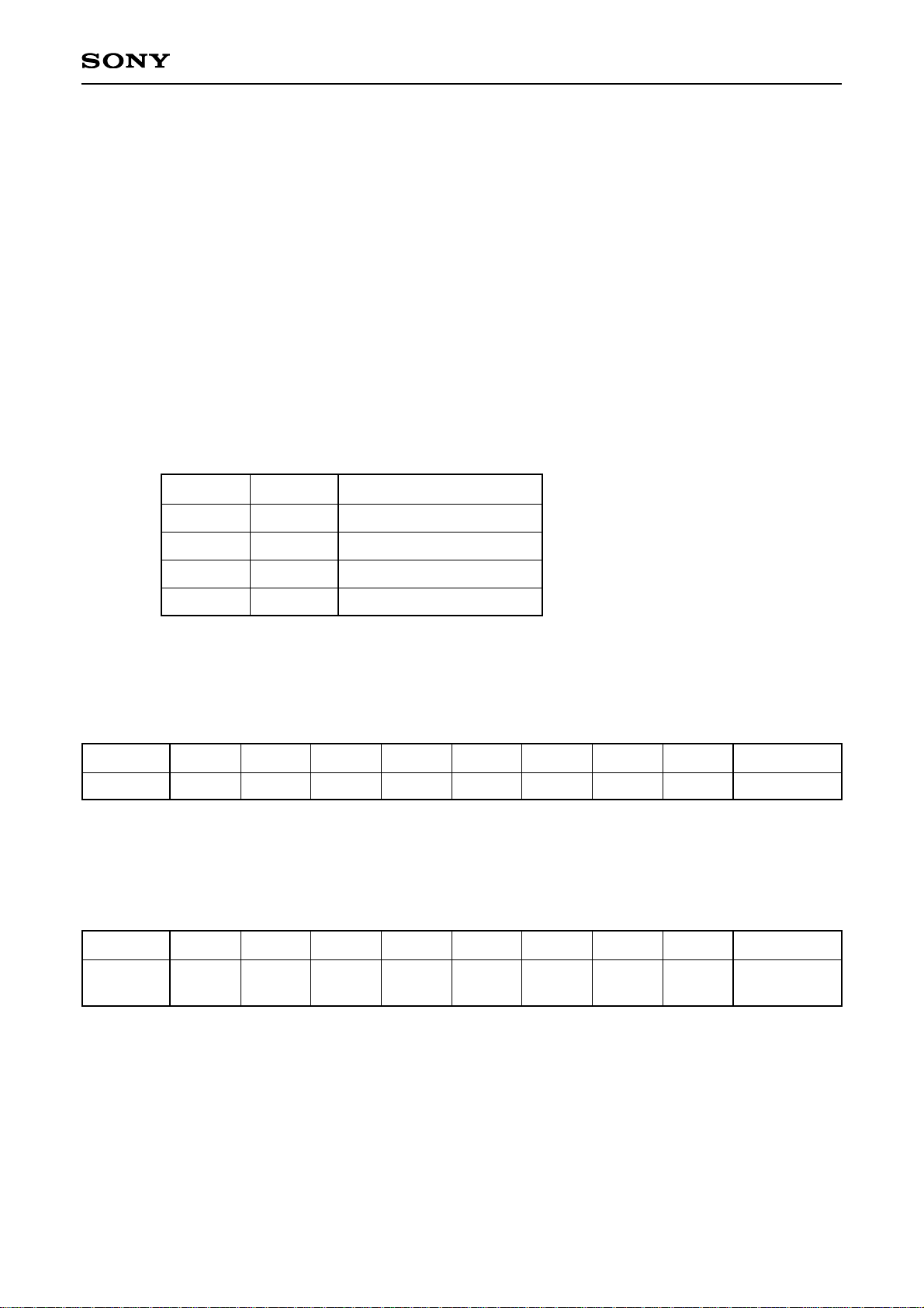
Electrical Characteristics (VDD = 5V ± 10%, VSS = 0V, Topr = –20 to +75°C)
Item
TTL input level pin
High level input voltage
TTL input level pin
Low level input voltage
CMOS input level pin
High level input voltage
CMOS input level pin
Low level input voltage
CMOS Schmitt input level pin
High level input voltage
CMOS Schmitt input level pin
Low level input voltage
CMOS Schmitt input level pin
Input voltage hysteresis
TTL Schmitt input level pin
High level input voltage
TTL Schmitt input level pin
Low level input voltage
TTL Schmitt input level pin
Input voltage hysteresis
SCSI Schmitt input level pin
High level input voltage
SCSI Schmitt input level pin
Low level input voltage
SCSI Schmitt input level pin
Input voltage hysteresis
Bidirectional pin with pull-up resistor
Input current
High level output voltage
High level output voltage
SCSI high level output voltage
Low level output voltage
SCSI low level output voltage
Input leakage current
Oscillation cell high level input voltage
Oscillation cell low level input voltage
Oscillation cell logic threshold value
Oscillation cell feedback resistance value
Oscillation cell high level output voltage
Oscillation cell low level output voltage
VIH1
VIL1
VIH2
VIL2
VIH4
VIL4
VIH4 – VIL4
VIH5
VIL5
VIH5 – VIL4
VIHS
VILS
VIHTS – VILTS
IIL3
VOH1
VOH2
VOHS
VOL1
VOLS
II1
VIH4
VIL4
LVTH
RFB
VOH3
VOL3
VIN = 0V
IOH = –2mA
IOH = –6mA
IOL = 4mA
IOL = 48mA
VIN = VSS or VDD
VIN = VSS or VDD
IOH = –12mA
IOL = 12mA
2.2
0.7VDD
0.8VDD
2.2V
2.2V
–90
VDD – 0.8
VDD – 0.8
2.5
–10
0.7VDD
250k
0.5VDD
0.6
0.4
0.4
–200
0.5VDD
1M
0.8
0.3VDD
0.2VDD
0.8V
0.8V
–440
3.7
0.4
0.5
10
0.3VDD
2.5M
0.5VDD
V
V
V
V
V
V
V
V
V
V
V
V
V
µA
V
V
V
V
V
µA
V
V
V
Ω
V
V
∗1
∗1
∗2
∗2
∗3
∗3
∗3
∗4
∗4
∗4
∗11
∗11
∗11
∗5
∗6
∗7
∗12
∗8
∗11
∗9
∗10
Symbol Conditions Min. Typ. Max. Unit
Applicable
pins
– 10 –
CXD1804BR
∗1
D7 to 0, MDBF to 0
∗2
MDAT, LRCK, C2PO, SBIN, SCOR, TD12 to 0
∗3
BLCK, WFCK, XRES
∗4
A6 to 0, XWR, XRD, XCS
∗5
D7 to 0, MDBF to 0
∗6
All output pins except XTL2, XRAS, XUCAS, XLCAS, XMWR and CLK
∗7
XRAS, XUCAS, XLCAS, XMWR, CLK
∗8
All output pins except XTL2
∗9
All input pins except ∗5and XTL1
∗10
Input: XTL1, Output: XTL2
∗11
XRST, XBSY, XSEL, XATN, XMSG, XCD, XIO, XREQ, XACK, XDBP, XDB7 to 0
∗12
XREQ, XACK, XDBP and XDB7 to 0 when active negation is ON
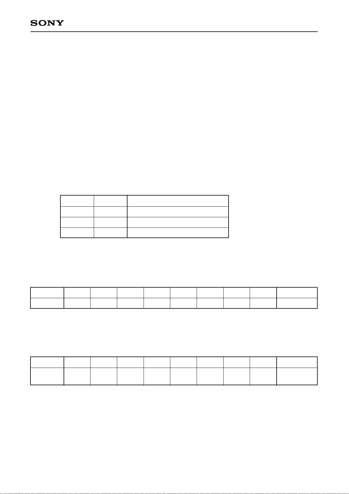
I/O Capacitance (VDD = VI = 0V, f = 1MHz)
Item
Input capacitance
Output capacitance
I/O capacitance
CIN
COUT
CI/O
9
11
11
pF
pF
pF
Symbol Min. Typ. Max. Unit
– 11 –
CXD1804BR
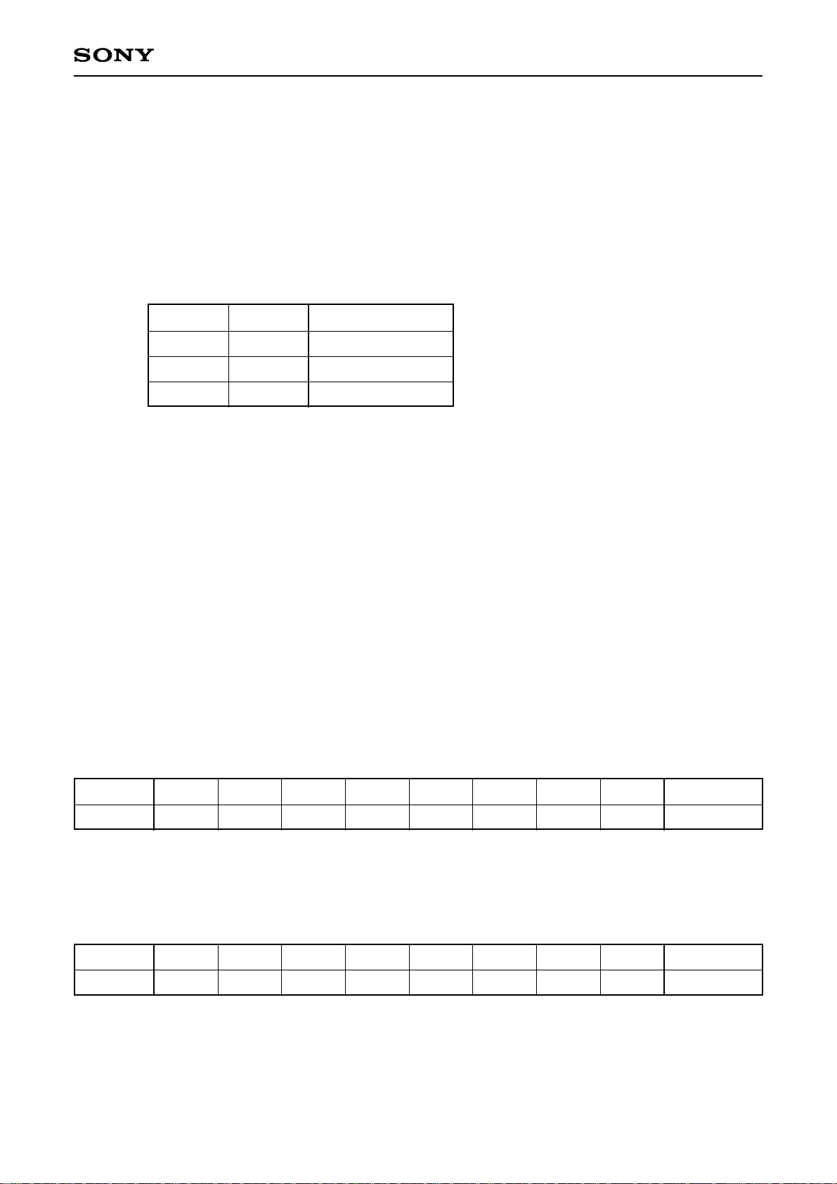
AC Characteristics
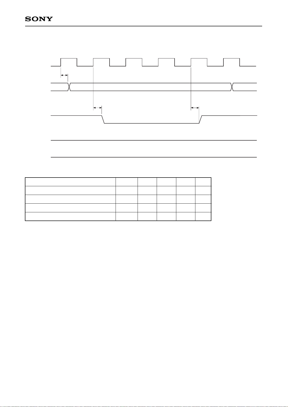
1. Sub CPU Interface (Output Load = 50pF)
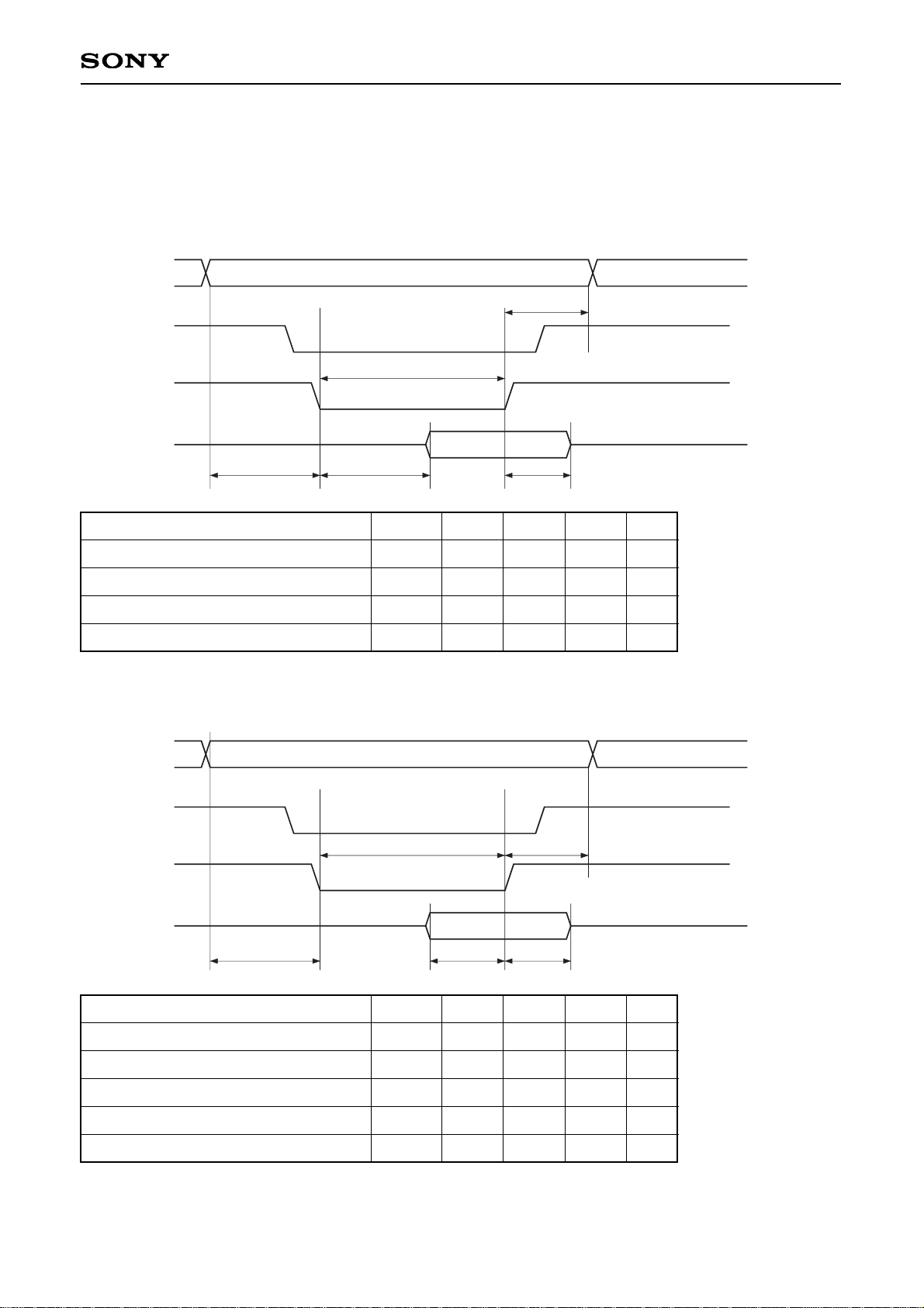
(1) Read
Tsar
Thar
A6 to 0
XCS
XRD
D7 to 0
Tdrd
Tfrd
Trrl
Item
Address setup time (for XCS & XRD ↓)
Address hold time (for XCS & XRD ↑)
Data delay time (for XCS & XRD ↓)
Data float time (for XCS & XRD ↑)
Tsar
Thar
Tdrd
Tfrd
10
10
0
35
15
ns
ns
ns
ns
Symbol Min. Typ. Max. Unit
Tsaw
Thwa
A6 to 0
XCS
XWR
D7 to 0
Tsdw Thdw
Twwl
Item
Address setup time (for XCS & XWR ↓)
Address hold time (for XCS & XWR ↑)
Data setup time (for XCS & XWR ↓)
Data hold time (for XCS & XWR ↑)
Low level XWR pulse width
Tsaw
Thaw
Tsdw
Thdw
Twwl
20
10
20
10
30
ns
ns
ns
ns
ns
Symbol Min. Typ. Max. Unit
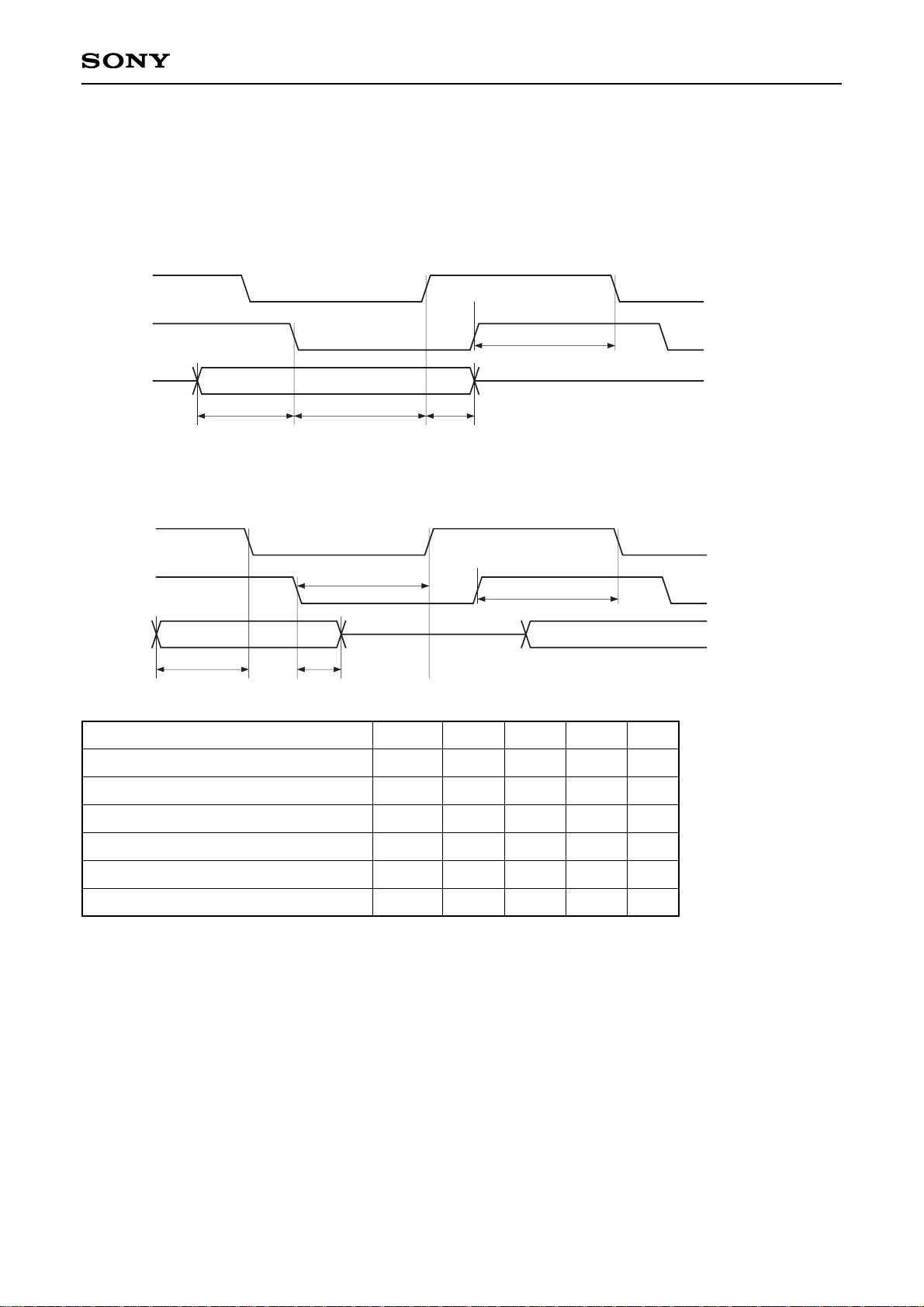
(2) Write
– 12 –
CXD1804BR
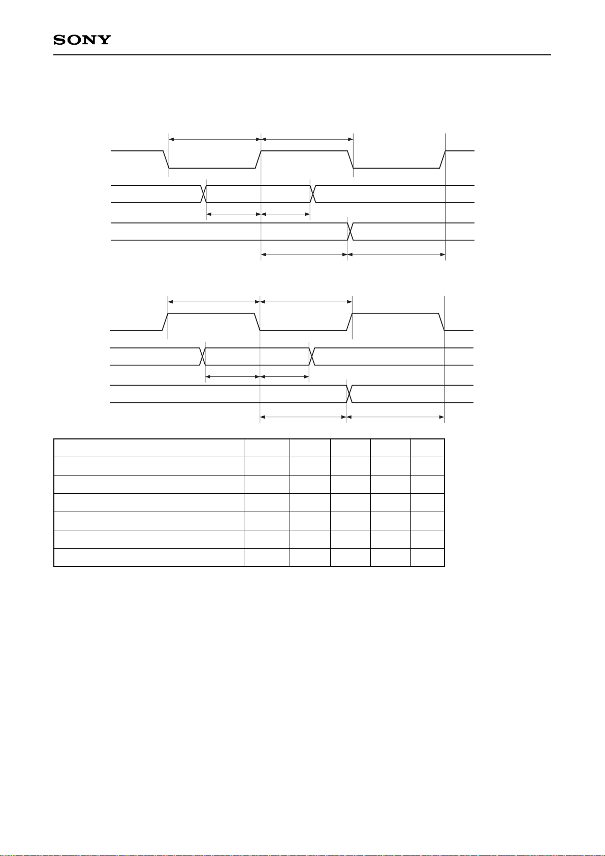
2. CD DSP Interface
BCKRED = "H"
Tbck Tbck
Tsb1
Thb1
Tsb2Thb2
BCLK
DATA
LRCK
C2PO
BCKRED = "L"
Tbck Tbck
Tsb1
Thb1
Tsb2Thb2
BCLK
DATA
LRCK
C2PO
Item
BCLK frequency
BCLK pulse width
DATA setup time (for BCLK)
DATA hold time (for BCLK)
LRCK, C2PO setup time (for BCLK)
LRCK, C2PO hold time (for BCLK)
Fbck
Tbck
Tsb1
Thb1
Tsb2
Thb2
19
10
10
10
10
26 MHz
ns
ns
ns
ns
ns
Symbol Min. Typ. Max. Unit
– 13 –
CXD1804BR
3. DRAM Interface (Output Load = 30pF)
(1) Read
Tma0
iCLK
Tma1
Trasl
Trash
Trc
Tcasl
Tcash
Tmdrs
Tmdrh
"H"
MA9 to 0
XRAS
XUCAS
XLCAS
XMWR
MDBF to 0
Item
Random read/write cycle time
Address delay time (for XTL2 ↑)
Address delay time (for XTL2 ↑)
XRAS ↓ delay time (for XTL2 ↑)
XRAS ↑ delay time (for XTL2 ↑)
XCAS ↓ delay time (for XTL2 ↑)
XCAS ↑ delay time (for XTL2 ↑)
Data setup time (for XTL2 ↑)
Data hold time (for XCAS ↑)
Trc
Tma0
Tma1
Trasl
Trash
Tcasl
Tcash
Tmdrs
Tmdrh
5Tw
13
11
6
6
7
6
2
0
24
22
12
11
14
12
4
45
41
23
20
25
22
6
ns
ns
ns
ns
ns
ns
ns
ns
ns
Symbol Min. Typ. Max. Unit
– 14 –
CXD1804BR
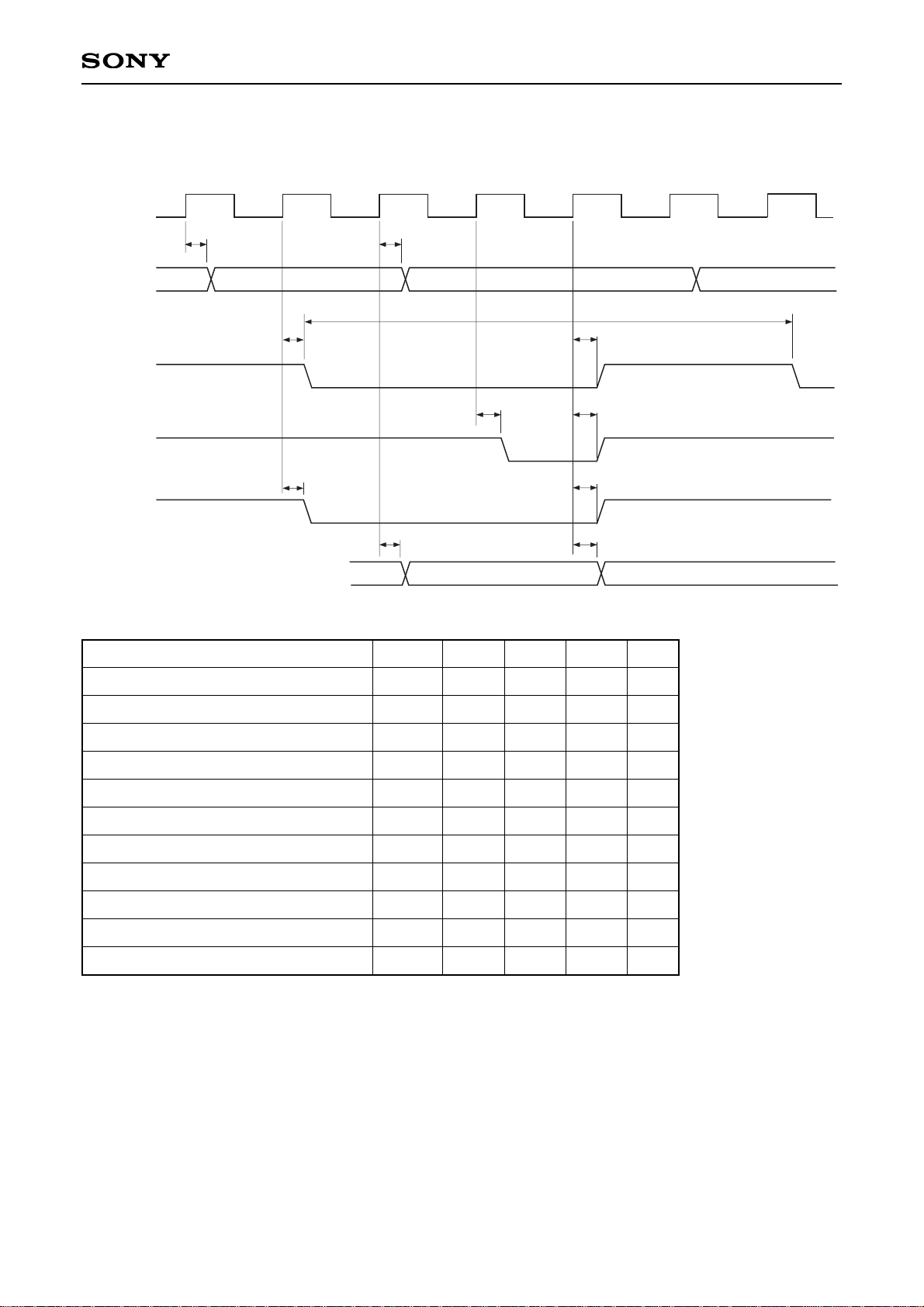
(2) Write
Tma0
iCLK
Tma1
Trasl
Trash
Trc
Tcash
Tcasl
Tmdws
MA9 to 0
XRAS
XUCAS
XLCAS
XMWR
MDBF to 0
Tmwrh
Tmwrl
Tmdwh
Item
Random read/write cycle time
Address delay time (for XTL2 ↑)
Address delay time (for XTL2 ↑)
XRAS ↓ delay time (for XTL2 ↑)
XRAS ↑ delay time (for XTL2 ↑)
XCAS ↓ delay time (for XTL2 ↑)
XCAS ↑ delay time (for XTL2 ↑)
XMWR ↓ delay time (for XTL2 ↑)
XMWR ↑ delay time (for XTL2 ↑)
Data setup time (for XTL2 ↑)
Data hold time (for XTL2 ↑)
Trc
Tma0
Tma1
Trasl
Trash
Tcasl
Tcash
Tmwrl
Tmwrh
Tmdws
Tmdwh
5Tw
13
11
6
6
7
6
7
6
14
7
24
22
12
11
14
12
14
11
28
14
45
41
23
20
25
22
25
21
51
26
ns
ns
ns
ns
ns
ns
ns
ns
ns
ns
ns
Symbol Min. Typ. Max. Unit
– 15 –
CXD1804BR
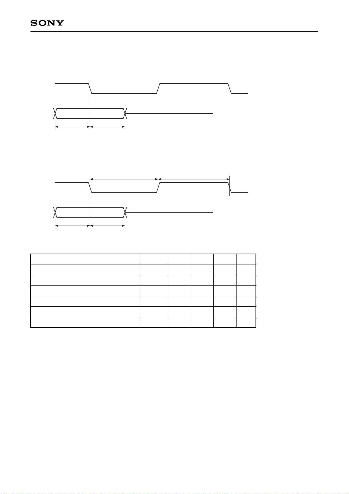
(3) Refresh (RAS only refresh)
Tma0
iCLK
Trasl
Trash
MA9 to 0
XRAS
XUCAS
XLCAS
XMWR
“H”
“H”
Item
Random read/write cycle time
Address delay time (for XTL2 ↑)
XRAS ↓ delay time (for XTL2 ↑)
XRAS ↑ delay time (for XTL2 ↑)
Trc
Tma0
Trasl
Trash
5Tw
12
6
6
24
12
11
43
23
20
ns
ns
ns
ns
Symbol Min. Typ. Max. Unit
– 16 –
CXD1804BR
4. SCSI Interface
(1) SCSI asynchronous transfer timing
When receiving: Initiator → Target
Taads Tardh
XREQ
XACK
XDB
Taaarnd
Taanrad
When transmitting: Target → Initiator
Tards
XREQ
XACK
XDB
Taadh
Taanrad
Taaarnd
Item
XDB setup time (for XACK ↓)
XDB hold time (for XREQ ↑)
XDB setup time (for XREQ ↓)
XDB hold time (for XREQ ↓)
XREQ rise delay time (for XACK ↓)
XREQ fall time (for XACK ↑)
Taads
Tardh
Tards
Taadh
Taaarnd
Taanrad
15
0
30
60
30
30
70
85
ns
ns
ns
ns
ns
ns
Symbol Min. Typ. Max. Unit
– 17 –
CXD1804BR
(2) SCSI synchronous transfer timing
When receiving: Initiator → Target
Tnads
XACK
XDB
Tnadh
When transmitting: Target → Initiator
Tnads
XREQ
XDB
Tnadh
Tnrap Tnrnp
Item
XDB setup time (for XACK ↓)
XDB hold time (for XACK ↓)
XDB setup time (for XREQ ↓)
XDB hold time (for XREQ ↓)
XREQ assert time
XREQ negate time
Tnads
Tnadh
Tnrds
Tnrdh
Tnrap
Tnrnp
15
10
80
105
90
110
ns
ns
ns
ns
ns
ns
Symbol Min. Typ. Max. Unit

– 18 –
CXD1804BR
(3) Fast SCSI synchronous transfer timing
When receiving: Initiator → Target
Tfads
XACK
XDB
Tfadh
When transmitting: Target → Initiator
Tfrds
XREQ
XDB
Tfrdh
Tfrap Tfrnp
Item
XDB setup time (for XACK ↓)
XDB hold time (for XACK ↓)
XDB setup time (for XREQ ↓)
XDB hold time (for XREQ ↓)
XREQ assert time
XREQ negate time
Tfads
Tfadh
Tfrds
Tfrdh
Tfrap
Tfrnp
15
10
55
55
40
60
ns
ns
ns
ns
ns
ns
Symbol Min. Typ. Max. Unit
– 19 –
CXD1804BR
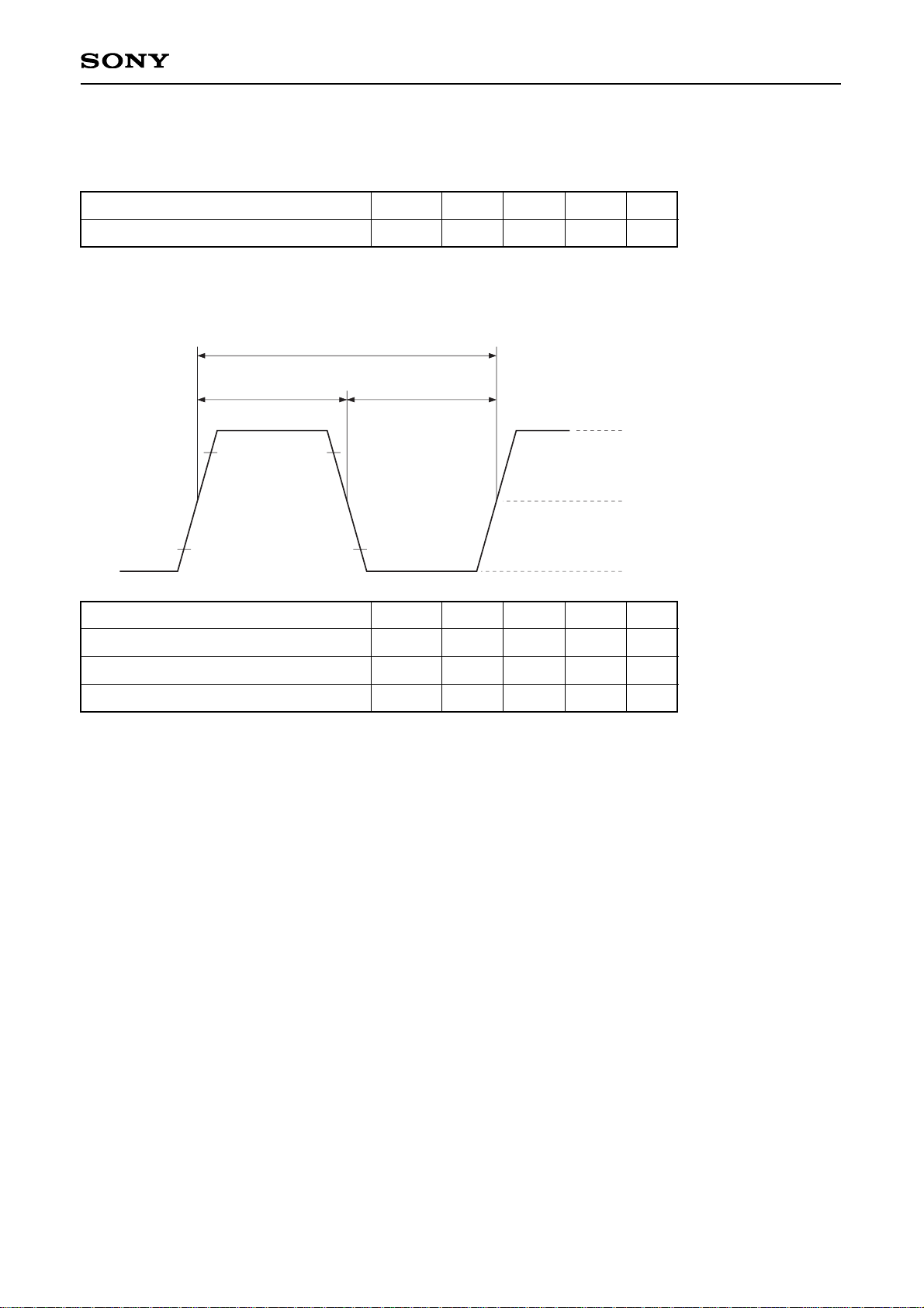
5. XTL1 and XTL2 Pins
(1) When using self-excited oscillation
Item
Oscillation frequency Fmax 40.0 MHz
Symbol Min. Typ. Max. Unit
Vihx
TwlxTwhx
Tw
V
DD/2
Vilx
(2) When inputting a pulse to the XTL1 pin
Item
High level pulse width
Low level pulse width
Pulse cycle
Twhx
Twhx
Tw
10
10
25
ns
ns
ns
Symbol Min. Typ. Max. Unit

– 20 –
CXD1804BR
Contents
[1] Description of Registers........................................................................................................................... 21
1-1. Description of Decoder Block Registers............................................................................................... 21
1-2. Description of SCSI2 Controller Block Registers.................................................................................. 46
1-3. Common Registers............................................................................................................................... 60
[2] Description of SCSI Controller Block Commands ................................................................................. 68
2-1. Precautions when Executing Commands............................................................................................. 69
2-2. Category 00 Commands....................................................................................................................... 69
2-3. Category 01 Commands....................................................................................................................... 74
2-4. Category 10 Commands....................................................................................................................... 76
2-5. Category 11 Commands....................................................................................................................... 79
[3] Appendix A................................................................................................................................................. 84
3-1. List of CD-ROM Decoder Block Registers............................................................................................ 84
3-2. List of SCSI Controller Block Registers................................................................................................ 90
3-3. List of Common Registers ....................................................................................................................94
3-4. Register Reset Conditions.................................................................................................................... 96
[4] Appendix B............................................................................................................................................... 102
4-1. Summary of SCSI Controller Block Commands ................................................................................. 102
– 21 –
CXD1804BR
[1] Description of Registers
The CXD1804AR's register address area is allotted as shown in the table below.
Address
00h to 4Fh
50h to 6Fh
70h to 7Fh
0xx xxxx
100 xxxx
101 xxxx
110 xxxx
111 xxxx
CD-ROM decoder block
SCSI2 interface block
CD-ROM decoder/SCSI2 interface common block
Description
1-1. Description of Decoder Block Registers
1-1-1. 00h
(1) RAWMIN (raw minute) register (read)
RAWMIN (raw minute) register
00h (R)
Adr. bit7 bit6 bit5 bit4 bit3 bit2 bit1 bit0 Reg.
REWMIN
The Header Minute byte for the sector being sent from the CD DSP while DECINT is active can be read from
this register. A difference of two sectors exists between the RAWxxx and BFxxx registers during the write-only
and real-time correction modes.
(2) CONFIG0 (configuration 0) register (write)
CONFIG0 (configuration 0) register
00h (W)
CINT
POL
RAM
SIZE1
RAM
SIZE0
RAM8
BITW
RAM2
CAS
EXCK
SEL
CLK
SEL1
CLK
SEL0
Adr. bit7 bit6 bit5 bit4 bit3 bit2 bit1 bit0 Reg.
CONFIG0
bit 7: CINTPOL (sub CPU interrupt polarity)
High: The INT pin becomes active high. When the register is inactive, it goes low.
Low: The INT pin becomes active low. When the register is inactive, it goes to high impedance.
bits 6, 5: RAMSIZE1, 0 (DRAM size 1, 0)
Set these bits according to the total size of the DRAM connected to this IC.
RAMSIZE1
"L"
"L"
"H"
"H"
"L"
"H"
"L"
"H"
1M bits
2M bits
4M bits
8M bits
RAMSIZE0 DRAM total size
bit 4: RAM8BITW (DRAM 8-bit wide)
This bit is set according to the bit width of the DRAM data bus to be connected.
High: Set this bit high when the DRAM to be connected has the 8-bit width.
Low: Set this bit low when the DRAM to be connected has the 16-bit width.
(Set low when two 8-bit width DRAMs are connected in parallel.)
– 22 –
CXD1804BR
bit 3: RAM2CAS (DRAM 2 CAS)
When the DRAM bus width is 16 bits, set this bit according to the number of CAS and WE signals.
When the DRAM bus width is 8 bits, this bit has no meaning.
High: Set this bit high when the IC is connected to a DRAM with 2 CAS signals and 1 WE signal.
Low: Set this bit low when the IC is connected to a DRAM with 1 CAS signal and 2 WE signals.
bit 2: EXCKSEL (EXCK select)
This bit determines the frequency of the EXCK clock that is used to get the subcode from the CD
DSP. This bit is set by the sub CPU on the basis of the playback speed and the clock frequency on
the XTL1 pin. (The maximum frequency for EXCK is 1MHz.)
High: The EXCK frequency is 1/48 the frequency of the XTL1 pin. Set this bit high when the XTL1
frequency is greater than 32MHz.
Low: The EXCK frequency is 1/32 the frequency of the XTL1 pin. Set this bit low when the XTL1
frequency is less than 32MHz.
bits 1, 0: CLKSEL1, 0 (CLK select 1, 0)
These bits determine the clock frequency output from the CLK pin.
CLKSEL1
"L"
"L"
"H"
"H"
"L"
"H"
"L"
"H"
Fixed to high
1/2 of XTL1
Same frequency as XTL1
RESERVED
CLKSEL0 Clock frequency
1-1-2. 01h
(1) RAWSEC (raw second) register (read)
RAWSEC (raw second) register
00h (R)
Adr. bit7 bit6 bit5 bit4 bit3 bit2 bit1 bit0 Reg.
RAWSEC
The Header Second byte for the sector being sent from the CD DSP while DECINT is active can be read from
this register.
(2) CONFIG1 (configuration 1) register (write)
CONFIG1 (configuration 1) register
00h (W)
SW
OPEN
SYC
NGC2
SYC
NGC1
SYC
NGC0
HWKR
QDIS
"L"
SBC
ECC1
SBC
ECC0
Adr. bit7 bit6 bit5 bit4 bit3 bit2 bit1 bit0 Reg.
CONFIG1
bit 7: SWOPEN (sync window open)
High: The Sync mark detection window opens. In this case, the IC's internal Sync protection circuit
is disabled.
Low: The Sync mark detection window is controlled by the IC's internal Sync protection circuit.
bits 6 to 4: SYCNGC2 to 0 (sync NG count 2 to 0)
The Sync mark detection window opens once the number of Sync marks specified by these bits is
inserted. Setting a value of 1h or less for these bits is prohibited. (After a reset, these bits are set to
2h.)
– 23 –
CXD1804BR
bit 3 HWKRQDIS (host DMA weak request disable)
High: (For the send system command passed through a buffer)
When the FIFO does not have eight empty bytes or more, the DMA does not start to the
FIFO from the buffer.
(For the receive system command passed through a buffer)
When the data of eight bytes or more are written (or the last data is written) in the FIFO, the
DMA starts to the buffer from the FIFO.
Low: (For the send system command passed through a buffer)
When the FIFO is not filled with data, the DMA starts to the FIFO from the buffer.
(For the receive system command passed through a buffer)
The DMA starts to the buffer from the FIFO immediately after the data are written in the
FIFO.
The number of times of the DMA execution for the host is reduced by setting this bit high.
(Because the page mode is always used.)
bit 2: RESERVED
Normally set low.
bits 1, 0: SBCECC1, 0 (subcode ECC 1, 0)
These two bits specify the error correction method when decoding the subcode.
SBECC1
"X"
"L"
"H"
"L"
"H"
"H"
Error correction not performed.
Single error correction performed.
Double error correction performed.
SBECC0 Subcode error correction
1-1-3. 02h
(1) RAWBLK (raw block) register (read)
RAWBLK (raw block) register
02h (R)
Adr. bit7 bit6 bit5 bit4 bit3 bit2 bit1 bit0 Reg.
RAWBLK
The Header Block byte for the sector being sent from the CD DSP while DECINT is active can be read from
this register.
(2) DSPIF (DSP interface) register (write)
DSPIF (DSP interface) register
02h (W)
C2PO
L1st
LCH
LOW
BCK
RED
BCKL
MD1
BCKL
MD0
LSB
1st
"L"
BFSH
DFSL
Adr. bit7 bit6 bit5 bit4 bit3 bit2 bit1 bit0 Reg.
DSPIF
This register controls the connection mode with the CD DSP. After the IC is reset, the sub CPU sets this
register according to the CD DSP to be connected.
bit 7: C2PL1ST (C2PO lower byte first)
High: When two bytes of data are input, C2PO inputs the lower byte first followed by the upper byte.
Low: When two bytes of data are input, C2PO inputs the upper byte first followed by the lower byte.
Here, "upper byte" means the upper 8 bits including MSB from the CD DSP and "lower byte"
means the lower 8 bits including LSB from the CD DSP. For example, the Header minute
byte is the lower byte and the second byte, the upper byte.
– 24 –
CXD1804BR
bit 2: LSB1ST (LSB first)
High: Connected with the CD DSP which outputs data with LSB first.
Low: Connected with the CD DSP which outputs data with MSB first.
bit 1: RESERVED
Normally set low.
Any change to the bits in this register must be made in the decoder disable status. (After the IC is
reset, the address is 28h.)
bit 0 BFSHDFSL (buffering subheader flag select)
High: The Sub Headers written two times are compared and, if they do not match, the result
reports an error to bits 3 to 0 of BFHDRFLG.
Low: When the C2PO of the Sub Headers written two times are both high, that reports an error to
the bits 3 to 0 of BFHDRFLG.
1-1-4. 03h
(1) RAWMD (raw mode) register (read)
RAWMD (raw mode) register
03h (R)
Adr. bit7 bit6 bit5 bit4 bit3 bit2 bit1 bit0 Reg.
RAWMD
The Header Mode byte for the sector being sent from the CD DSP while DECINT is active can be read from
this register.
(2) RFINTVL (refresh interval) register (write)
RFINTVL (refresh interval) register
03h (W) b7 b6 b5 b4 b3 b2 b1 b0
Adr. bit7 bit6 bit5 bit4 bit3 bit2 bit1 bit0 Reg.
RFINTVL
This register determines the refresh interval. The refresh interval is RFINTVL × 4 × TW. Here, TW represents
the XTL1 clock frequency. Note that this IC performs RAS only refresh.
bit 6: LCHLOW (Lch low)
High: When LRCK is low, determined to be the left channel data.
Low: When LRCK is high, determined to be the right channel data.
bit 5: BCKRED (BLCK rising edge)
High: Data is strobed at the rising edge of BCLK.
Low: Data is strobed at the falling edge of BCLK.
bits 4, 3: BCKMD1, 0 (BCLK mode 1, 0)
These bits are set according to the number of clocks output for BCLK during 1/2 LCLK cycle by the
CD digital signal processing LSI (CD DSP).
BCKMD1
"L"
"L"
"H"
"L"
"H"
"X"
16BCLKs/WCLK
24BCLKs/WCLK
32BCLKs/WCLK
BCKMD0
– 25 –
CXD1804BR
bits 7, 6: DSTBSL1, 0
These bits determine the frequency of the DSTB and XLAT clocks used for passing data (DATO) to
the CD DSP. The sub CPU sets these bits according to the frequency of the clock on the XTL1 pin.
(The maximum frequency for DSTB is 1MHz.)
DSTBDL1
0
0
1
1
0
1
0
1
1/24 of XTL1
1/32 of XTL1
1/48 of XTL1
1/64 of XTL1
DSTBDL0 Frequency
bit 5: DISXLAT (disable XLAT output)
High: After the contents of the DSPCMD register are transferred to the DSP, a latch pulse is not
output from the XLAT pin. In this case, the sub CPU uses DSPCMDLT (bit 0 of the
CHPCTL0 register) to output a latch pulse from the XLAT pin at the appropriate time.
Low: After the contents of the DSPCMD register are transferred to the DSP, a latch pulse is output
from the XLAT pin.
bits 4, 3: XFRBYT1, 0 (transfer command byte length 1,0)
These bits determine the number of bytes in the command data (DSPCMD register) to be
transferred to the CD DSP. The relationship between the settings and the number of transferred
bytes is shown in the following table.
XFRBYT1
"L"
"L"
"H"
"H"
"L"
"H"
"L"
"H"
Prohibited
1
2
3
XFRBYT0 Number of transferred bytes
1-1-5. 04h
(1) BFMIN (buffer minute) register (read)
BFMIN (buffer minute) register
04h (R)
Adr. bit7 bit6 bit5 bit4 bit3 bit2 bit1 bit0 Reg.
BFMIN
During the execution of a write-only or real-time error correction command and after execution of a repeat
correction command, the Header Minute byte of the current sector can be read from this register. This register
is invalid when the decoder is disabled or a monitor-only command is being executed.
(2) DSPCTL (DSP control) register (write)
DSPCTL (DSP control) register
04h (W)
DSTB
SL1
DSTB
SL0
DIS
XLAT
XFR
BYT1
XFR
BYT0
FAST
DSTB
SBAI
TMSL
FAST
EXCK
Adr. bit7 bit6 bit5 bit4 bit3 bit2 bit1 bit0 Reg.
DSPCTL
– 26 –
CXD1804BR
1-1-7. 06h
(1) BFHDRBLK (buffer header block) register (read)
BFHDRBLK (buffer block) register
06h (R)
Adr. bit7 bit6 bit5 bit4 bit3 bit2 bit1 bit0 Reg.
BFHDRBLK
During the execution of a write-only or real-time error correction command and after execution of a repeat
correction command, the Header Block byte of the current sector can be read from this register. This register is
invalid when the decoder is disabled or a monitor-only command is being executed.
bit 1 SBAITMSL (subcode buffering area increment timing select)
High: The internal subcode buffering area is incremented when the first pack of data is retrieved
and de-interleaving is performed.
Low: The internal subcode buffering are is incremented when the subcode Sync mark is detected
and inserted.
bit 0 FASTEXCK (fast EXCK)
High: The EXCK frequency is 1/8 the frequency of the XTL1 pin.
Low: The EXCK frequency depends on the settings of EXCKSEL (CONFIG0 bit 2)
1-1-6. 05h
(1) BFSEC (buffer second) register (read)
BFSEC (buffer second) register
05h (R)
Adr. bit7 bit6 bit5 bit4 bit3 bit2 bit1 bit0 Reg.
BFSEC
During the execution of a write-only or real-time error correction command and after execution of a repeat
correction command, the Header Second byte of the current sector can be read from this register. This register
is invalid when the decoder is disabled or a monitor-only command is being executed.
(2) DSPCMD (DSP command) register (write)
DSPCMD (DSP command) register
05h (W) b7 b6 b5 b4 b3 b2 b1 b0
Adr. bit7 bit6 bit5
bit4
bit3 bit2 bit1 bit0 Reg.
DSPCMD
The data to be serially transferred to the CD DSP is written in this register. This register is a three-byte LIFO
(last-in, first-out) register.
bits 2: FASTDSTB
When this bit is high, it is possible to make the frequencies faster of the DSTB, DATO and XLAT
outputs to the CD DSP set in DSTBSL1 and 0 (DSPCTL bits 7 and 6).
DSTBSL1
0
0
1
1
0
1
0
1
1/48 of XTL1
1/16 of XTL1
1/8 of XTL1
1/4 of XTL1
DSTBSL0 Frequency
– 27 –
CXD1804BR
07h (R)
Adr. bit7 bit6 bit5 bit4 bit3 bit2 bit1 bit0 Reg.
BFMD
During the execution of a write-only or real-time error correction command and after execution of a repeat
correction command, the Header Mode byte of the current sector can be read from this register. This register is
invalid when the decoder is disabled or a monitor-only command is being executed.
1-1-11. 0Ah
(1) BFSUBM (buffer sub mode) register (read)
BFSUBM (buffer sub mode) register
0Ah (R)
Adr. bit7 bit6 bit5 bit4 bit3 bit2 bit1 bit0 Reg.
BFSUBM
During the execution of a write-only or real-time error correction command and after execution of a repeat
correction command, the Sub Header Sub Mode byte of the current sector can be read from this register. This
register is invalid when the decoder is disabled or a monitor-only command is being executed.
1-1-9. 08h
(1) BFFILE (buffer file) register (read)
BFFILE (buffer file) register
08h (R)
Adr. bit7 bit6 bit5 bit4 bit3 bit2 bit1 bit0 Reg.
BFFILE
During the execution of a write-only or real-time error correction command and after execution of a repeat
correction command, the Sub Header File byte of the current sector can be read from this register. This
register is invalid when the decoder is disabled or a monitor-only command is being executed.
1-1-10. 09h
(1) BFCHAN (buffer channel) register (read)
BFCHAN (buffer channel) register
09h (R)
Adr. bit7 bit6 bit5 bit4 bit3 bit2 bit1 bit0 Reg.
BFCHAN
During the execution of a write-only or real-time error correction command and after execution of a repeat
correction command, the Sub Header Channel byte of the current sector can be read from this register. This
register is invalid when the decoder is disabled or a monitor-only command is being executed.
1-1-8. 07h
(1) BFMD (buffer mode) register (read)
BFMD (buffer mode) register
– 28 –
CXD1804BR
1-1-13. 0Ch
(1) RAWHDRFLG (raw header flag) register (read)
RAWHDRFLG (raw header flag) register
0Ch (R) MIN SEC
BLO
CK
MODE
CDR
DTEN
Adr. bit7 bit6 bit5 bit4 bit3 bit2 bit1 bit0 Reg.
RAWHDR
This register indicates the C2PO value for the RAWHDR register.
bit 7 Minute
bit 6 Second
bit 5 Block
bit 4 Mode
bit 3 to 1 RESERVED
bit 0 CD-R Mode Detect Enable
(2) CDRMOD (CD-R mode) register (write)
CDRMOD (CD-R mode) register
bit 0 CDRDTEN (CD-R mode detect enable)
High: The CDRINT status results when the decoder is operating in the monitor-only, write-only,
real-time correction or asynchronous correction mode if either of the conditions below is met.
(1) Bits 7 to 5 of the Raw Mode byte are not "000".
(2) The error flag of the Raw Mode byte is not established. (Values after processing by
setting of MDBYTCTL (DECCTL0 bit 2))
Low: The CD-R Mode byte is not detected.
1-1-14. 0Dh
(1) BFHDRFLG (buffer header flag) register (read)
BFHDRFLG (buffer header flag) register
0Dh (R) MIN SEC
BLO
CK
MODE FILE CHAN
SUB
MODE
DATA
TYPE
Adr. bit7 bit6 bit5 bit4 bit3 bit2 bit1 bit0 Reg.
HDRFLG
0Ch (W)
CDR
DTEN
Adr. bit7 bit6 bit5 bit4 bit3 bit2 bit1 bit0 Reg.
CDRMODE
0Bh (R)
Adr. bit7 bit6 bit5 bit4 bit3 bit2 bit1 bit0 Reg.
BFDTYP
During the execution of a write-only or real-time error correction command and after execution of a repeat
correction command, the Sub Header Data Type byte of the current sector can be read from this register. This
register is invalid when the decoder is disabled or a monitor-only command is being executed.
1-1-12. 0Bh
(1) BFDTYP (buffer data type) register (read)
BFDTYP (buffer data type) register
– 29 –
CXD1804BR
This register shows the error status of each byte in the BFHDR and BFSHDR registers. High means an error.
bit7 Minute
bit6 Second
bit5 Block
bit4 Mode
bit3 File
bit2 Channel
bit1 Submode
bit0 Data Type
1-1-15. 0Eh
(1) DECSTS0 (decoder status 0) register (read)
DECSTS0 (decoder status 0) register
0Eh (R)
Adr. bit7 bit6 bit5 bit4 bit3 bit2 bit1 bit0 Reg.
DECSTS0
bit 7: SHRTSCT (short sector)
Indicates that the Sync mark interval was less than 2351 bytes since the previous DECINT. This
sector does not remain in the buffer memory.
bit 6: NOSYNC
Indicates that the Sync mark was inserted because one was not detected in the prescribed position
for the current sector.
bit 5: CORINH (correction inhibit)
This is high if the current sector Mode and Form could not be determined when the AUTODIST bit
of the DECCTL register is set high. ECC or EDC is not executed in this sector. The CORINH bit is
invalid when AUTODIST is set low. It is high in any of the conditions below when the AUTODIST bit
is set high.
(1) When an error was found in the Mode byte.
(2) When the Mode byte is a value other than 01h or 02h.
(3) When the Mode byte is 02h and the C2 pointer is high in the Submode byte.
bit 4: ERINBLK (erasure in block)
When the decoder is operating in the monitor-only, write-only or real-time mode which prohibits
erasure correction, this indicates that at least a 1-byte error flag (C2PO) has been raised in the
data excluding the Sync mark from the current sector CD DSP.
bit 3: CORDONE (correction done)
Indicates that there is an error corrected byte in the current sector.
bit 2: EDCNG
Indicates that an error was found in the current sector through an EDC check.
bit 1: ECCNG
Indicates that an uncorrectable error was found somewhere between the Header byte and the
Parity byte in the current sector. (Bit 1 = don't care in the Mode2, Form2 sectors.)
bit 0: TGTNTMET (target not met)
Indicates that the current sector address and the target address in the TGTMNT, TGTSEC, and
TGTBLK registers do not match. The error pointer is not referenced in this instance.
– 30 –
CXD1804BR
1-1-16. 0Fh
(1) DECSTS1 (decoder status 1) register (read)
DECSTS1 (decoder status 1) register
0Fh (R)
Adr. bit7 bit6 bit5 bit4 bit3 bit2 bit1 bit0 Reg.
DECSTS1
bits 7 to 3: RESERVED
bit 2: EDCALL0 (EDC all 0)
This is high when there are no error flags in all the 4 EDC parity bytes of the current sector and
their values are all 00h.
bit 1: CMODE (correction mode)
bit 0: CFORM (correction form)
These bits indicate the Mode and Form of the current sector the decoder has discriminated to
correct errors when the decoder is operating in the real-time correction or repeat correction mode.
CFORM
"X"
"L"
"H"
"L"
"H"
"H"
MODE1
MODE2, FORM1
MODE2, FORM2
CMODE
1-1-17. 10h, 11h
(1) LSTARA-H, L (last area-high, low) register (read/write)
LSTARA-H, L (last area-high, low) register
10h (R/W)
11h (R/W) b7 b6 b5 b4 b3 b2 b1
b8
b0
Adr. bit7 bit6 bit5 bit4 bit3 bit2 bit1 bit0 Reg.
LSTARA-H
LSTARA-L
This register specifies the last order area. Set bits 7 to 1 of the LSTARA-H register low when writing in this
register.
1-1-18. 12h, 13h
(1) LHADR-H, L (last HADR-high, low) register (read/write)
LHADR-H, L (last HADR-high, low) register
12h (R/W)
13h (R/W) b7 b6 b5 b4 b3 b2 b1
b8
b0
Adr. bit7 bit6 bit5 bit4 bit3 bit2 bit1 bit0 Reg.
LHADR-H
LHADR-L
When host automatic transfer mode is disabled, this register specifies the upper limit for HADRC (the upper 9
bits); for the subcode buffering command, this register specifies the upper limit for the address (upper 9 bits).
The lower 11 bits are 7FFh. Set bits 7 to 1 of the LHADR-H register low when writing in this register.
 Loading...