

Sony CXD1803AR, CXD1803AQ Datasheet

CXD1803AQ/AR
For the availability of this product, please contact the sales office.
CD-ROM DECODER
Description
CXD1803AQ/AR is a CD-ROM decoder LSI with a
built-in ADPCM decoder.
Features
• Compatible with CD-ROM, CD-I and CD-ROM XA
formats
• Real time error correction
• Capable of handling up to quadruple speed
playback
• Connectable with standard SRAM of up to 2M-bit
(256K-byte)
• Connectable with standard DRAM of up to 2M-bit
(256K-byte)
(2 DRAM's of 256K × 4)
• All audio output sampling frequencies: 132.3 KHz
(built-in oversampling filter)
• De-emphasis digital filter
• Digital attenuator
• Connectable directly with Sony's SCSI controller
CXD1185CQ.
CXD1803AQ CXD1803AR
100 pin QFP (Plastic) 100 pin LQFP (Plastic)
Absolute Maximum Ratings (Ta=25°C)
• Supply voltage VDD –0.5 to +7.0 V
• Input voltage VI –0.5 to VDD +0.5 V
• Output voltage VI –0.5 to VDD +0.5 V
• Operating temperature Topr –20 to +75 °C
• Storage temperature Tstg –55 to +150 °C
Recommended Operating Conditions
• Supply voltage VDD
+3.5 to +5.5 (+5.0 typ.) V
• Operating temperature Topr –20 to +75 °C
Applications
CD-ROM drives
Structure
Silicon gate CMOS IC
Sony reserves the right to change products and specifications without prior notice. This information does not convey any license by
any implication or otherwise under any patents or other right. Application circuits shown, if any, are typical examples illustrating the
operation of the devices. Sony cannot assume responsibility for any problems arising out of the use of these circuits.
—1—
E94Y31-TE
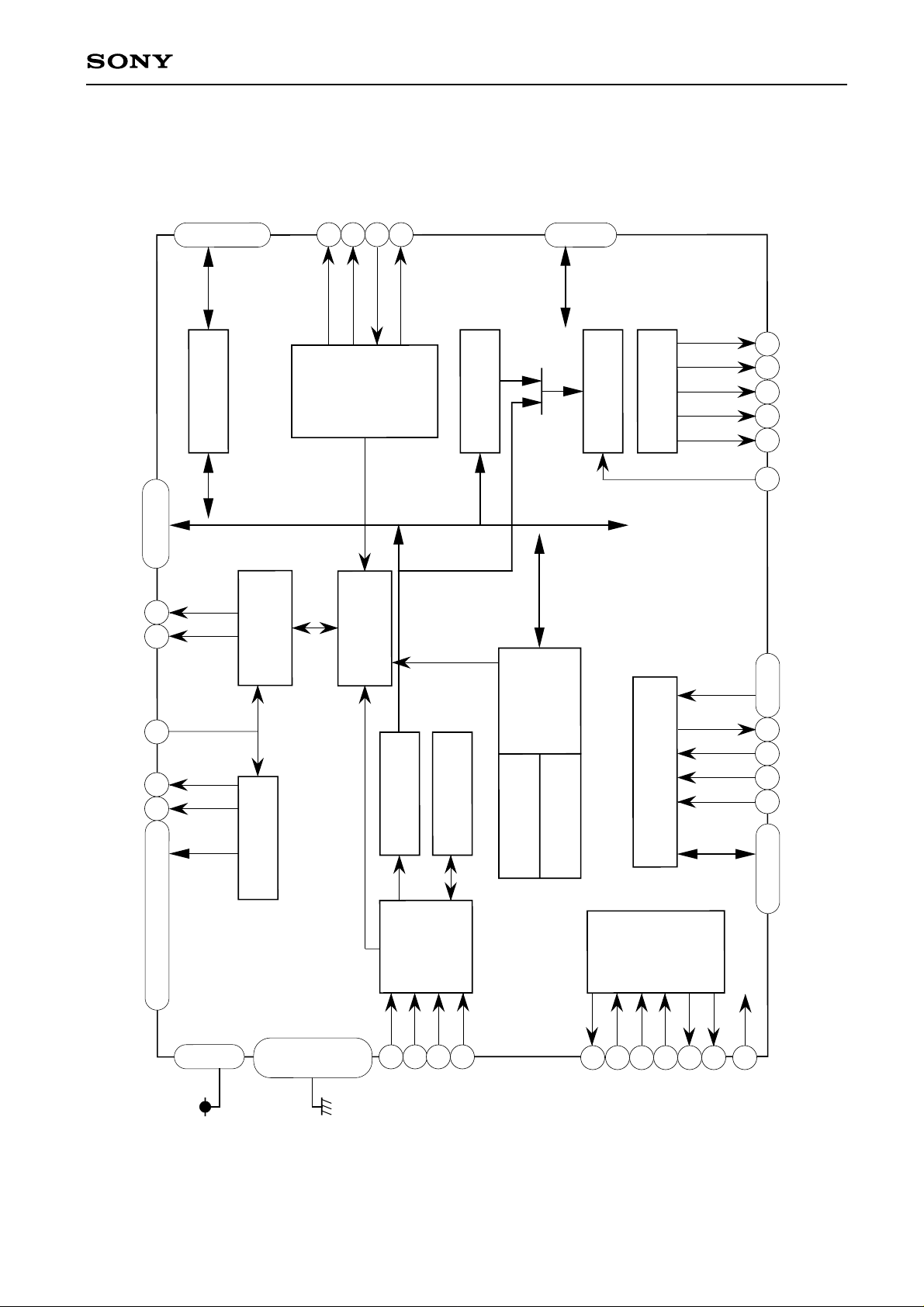
SD0-7
26
27
DMA FIFO
30
CXD1803AQ/AR
XSRD
XSWR
SDRQ
XSAC
|
34
36
24
37
25
HOST I/F
38
ADPCM DECODER
23
TD0-5
96
|
100
DAC I/F
DIGITAL FILETER
95
94
93
92
91
88
MUTE
BCKO
WCKO
LRCO
EMP DATO
MDB0-7,P
XMWR
XMOE
DRAM
XME1
XME0
MA0-16
66—70,72—75
64
63
21
62
57
DMA
SEQUENCER
ADDRESS GEN
PRIORITY
RESOLVER
DESCRAMBLER
SYNC CONTROL
CDP I/F
ECC
CORRECTOR
GALOIS FIELD
SYNDROME GEN
C
L G
Sub CPU I/F
O E
C N
K
A0-A4
17–20,22
16
XINT
14
XWR
13
XRD
12
XCS
D0-7
1,2,5–8,10,11
39,41—46,48—52,55,56,58,59,61
3
Block Diagram
28
53
VDD
78
4, 9
15,21
29,35
40,47
54,60
GND
65,71
79,90
84
LRCK
85
DATA
86
BCLK
—2—
87
C2PO
76
XTL2
77
XTL1
82
CKSL
83
RMCK
CLK
80
81
HCLK
89
XRST
The pin numbers in the diagram are for the CXD1803AQ.

Pin Description
CXD1803AQ/AR
Pin No.
QR
1 99 D0 I/O Sub CPU data bus
2 100 D1 I/O Sub CPU data bus
31 VDD — Power supply (+5 V)
4 2 GND — Ground
5 3 D2 I/O Sub CPU data bus
6 4 D3 I/O Sub CPU data bus
7 5 D4 I/O Sub CPU data bus
8 6 D5 I/O Sub CPU data bus
9 7 GND — Ground
10 8 D6 I/O Sub CPU data bus
11 9 D7 I/O Sub CPU data bus
12 10 XCS I IC select negative logic signal from sub CPU
13 11 XRD I Strobe negative logic signal to read this IC internal register from sub CPU
14 12 XWR I Strobe negative logic signal to write this IC internal register from sub CPU
15 13 GND — Ground
16 14 XINT O Interrupt request negative logic signal from IC to sub CPU
17 15 A0 I Sub CPU address
18 16 A1 I Sub CPU address
19 17 A2 I Sub CPU address
20 18 A3 I Sub CPU address
21 19 DRAM I Memory type selection signal. High: DRAM, Low: SRAM
22 20 A4 I Sub CPU address
23 21 TD0 I/O Test input/output
24 22 XSRD O Strobe negative logic signal to read SCSI controller internal register
25 23 XSWR O Strobe negative logic signal to write SCSI controller internal register
26 24 SD0 I/O SCSI controller data bus
27 25 SD1 I/O SCSI controller data bus
28 26 VDD — Power supply (+5 V)
29 27 GND — Ground
30 28 SD2 I/O SCSI controller data bus
31 29 SD3 I/O SCSI controller data bus
32 30 SD4 I/O SCSI controller data bus
33 31 SD5 I/O SCSI controller data bus
34 32 SD6 I/O SCSI controller data bus
Symbol I/O Description
—3—

CXD1803AQ/AR
Pin No.
QR
35 33 GND — Ground
36 34 SD7 I/O SCSI controller data bus
37 35 SDRQ I SCSI data request positive logic signal
38 36 XSAC O SCSI acknowledge negative logic signal
39 37 MA0 O Buffer memory address (LSB)
40 38 GND — Ground
41 39 MA1 O Buffer memory address
42 40 MA2 O Buffer memory address
43 41 MA3 O Buffer memory address
44 42 MA4 O Buffer memory address
45 43 MA5 O Buffer memory address
46 44 MA6 O Buffer memory address
47 45 GND — Ground
48 46 MA7 O Buffer memory address
49 47 MA8 O Buffer memory address
50 48 MA9 O Buffer memory address
51 49 MA10 O Buffer memory address
52 50 MA11 O Buffer memory address
53 51 VDD — Power supply (+5 V)
54 52 GND — Ground
55 53 MA12 O Buffer memory address
56 54 MA13 O Buffer memory address
57 55 XME0 O Memory chip enable negative logic signal
58 56 MA14 O Buffer memory address
59 57 MA15 O Buffer memory address
60 58 GND — Ground
61 59
62 60 XME1 O Memory chip enable negative logic signal
63 61
64 62 XMWR O Buffer memory write enable negative logic signal
65 63 GND — Ground
66 64 MDB0 I/O Buffer memory data bus
67 65 MDB1 I/O Buffer memory data bus
Symbol I/O Description
MA16
XRAS DRAM RAS signal
XMOE
XCAS DRAM CAS signal
Buffer memory address
O
Buffer memory output enable negative logic signal
O
—4—
CXD1803AQ/AR
Pin No.
QR
68 66 MDB2 I/O Buffer memory data bus
69 67 MDB3 I/O Buffer memory data bus
70 68 MDB4 I/O Buffer memory data bus
71 69 GND — Ground
72 70 MDB5 I/O Buffer memory data bus
73 71 MDB6 I/O Buffer memory data bus
74 72 MDB7 I/O Buffer memory data bus
75 73 MDBP I/O Buffer memory data bus (for error flag)
76 74 XTL2 O Crystal oscillation circuit output
77 75 XTL1 I Crystal oscillation circuit input (16.9344 MHz)
78 76 VDD — Power supply (+5 V)
79 77 GND — Ground
80 78 CLK O 16.9344 MHz clock output
81 79 HCLK O 8.4672 MHz clock output
82 80 CKSL I Clock select signal for CD-ROM decoder
83 81 RMCK I Clock signal for CD-ROM decoder
84 82 LRCK I LR clock signal from CD DSP (for discriminating L, R channels )
85 83 DATA I Data signal from CD DSP
86 84 BCLK I DATA pin strobe clock signal (bit clock)
87 85 C2PO I Error flag (C2 pointer) positive logic signal from CD DSP
88 86 EMP I Emphasis on positive logic signal from CD DSP
89 87 XRST I Reset negative logic signal
90 88 GND — Ground
91 89 DATO O Data signal to DAC (D/A converter)
92 90 LRCO O LR clock signal to DAC
93 91 WCKO O Word lock signal to DAC
94 92 BCKO O Bit clock signal to DAC
95 93 MUTE O Mute positive logic signal
96 94 TD5 I/O Test input/output
97 95 TD4 I/O Test input/output
98 96 TD3 I/O Test input/output
99 97 TD2 I/O Test input/output
100 98 TD1 I/O Test input/output
Symbol I/O Description
Note: The pin numbers in the column "Q" are for the CXD1803AQ, and those in the column "R" are for the
CXD1803AR.
—5—
CXD1803AQ/AR
Electrical Characteristics
DC Characteristics (VDD = 5 V ± 10%, VSS = 0 V, Topr = –20 - 75°C)
Item Symbol Conditions Min. Typ. Max. Unit
TTL input level pin ∗1
High level input voltage
TTL input level pin ∗1
Low level input voltage
CMOS input level pin ∗2
High level input voltage
CMOS input level pin ∗2
Low level input voltage
CMOS Schmitt input level pin ∗3
High level input voltage
CMOS Schmitt input level pin ∗3
Low level input voltage
CMOS Schmitt input level pin ∗3
Input voltage hysteresis
TTL Schmitt input level pin ∗4
High level input voltage
TTL Schmitt input level pin ∗4
Low level input voltage
TTL Schmitt input level pin ∗4
Input voltage hysteresis
Bidirectional pin with pull-up resistor ∗5
Input current
Pin with pull-up resistor ∗6
Input current
IH1 2.2 V
V
IL1 0.8 V
V
IH2 0.7VDD V
V
IL2 0.3VDD V
V
IH4 0.8VDD V
V
IL4 0.2VDD V
V
IH4 to VIL4 0.6 V
V
IH5 2.2V V
V
IL5 0.8V V
V
IH4 to VIL4 0.4 V
V
IL3 VIN=0V –90 –200 –440 µA
I
IL4 VIN=0V –40 –100 –240 µA
I
High level output voltage ∗7 VOH1 IOH=–2mA VDD-0.8 V
Low level output voltage ∗7 V
Input leakage current ∗8II1
Output leakage current ∗9IOZ
Oscillation cell ∗10 high level input voltage V
Oscillation cell low level input voltage V
Oscillation cell logic threshold value LV
Oscillation cell feedback resistance value RFB
Oscillation cell
High level output voltage
Oscillation cell
Low level output voltage
OL1 IOL=–4mA 0.4 V
VIN=VSS
or V
DD
High-impedance
state
IH4 0.7VDD V
IL4 0.3VDD V
TH 0.5VDD V
VIN=VSS
or V
DD
OH2 IOH=–3mA 0.5VDD V
V
OL2 IOL=3mA 0.5VDD V
V
–10 10 µA
–40 40 µA
250K 1M 2.5M Ω
—6—
DC Characteristics
Item Symbol Conditions Min. Typ. Max. Unit
CXD1803AQ/AR
(VDD = 3.5 V, VSS = 0 V, Topr = –20 - 75°C)
TTL input level pin ∗1
High level input voltage
TTL input level pin ∗1
Low level input voltage
CMOS input level pin ∗2
High level input voltage
CMOS input level pin ∗2
Low level input voltage
CMOS Schmitt input level pin ∗3
High level input voltage
CMOS Schmitt input level pin ∗3
Low level input voltage
CMOS Schmitt input level pin ∗3
Input voltage hysteresis
TTL Schmitt input level pin ∗4
High level input voltage
TTL Schmitt input level pin ∗4
Low level input voltage
TTL Schmitt input level pin ∗4
Input voltage hysteresis
Bidirectional pin with pull-up resistor ∗5
Input current
Pin with pull-up resistor ∗6
Input current
IH1 2.2 V
V
IL1 0.6 V
V
IH2 0.7VDD V
V
IL2 0.3VDD V
V
IH4 0.8VDD V
V
IL4 0.2VDD V
V
IH4 to VIL4 0.5 V
V
IH5 2.2V V
V
IL5 0.6V V
V
IH5 to VIL4 0.3 V
V
IL3 VIN=0V –20 –50 –110 µA
I
IL4 VIN=0V –10 –25 –60 µA
I
High level output voltage ∗7VOH1 IOH=–1.6mA VDD-0.8 V
Low level output voltage ∗7V
Input leakage current ∗8 II1
Output leakage current ∗9IOZ
Oscillation cell ∗10 high level input voltage V
Oscillation cell low level input voltage V
Oscillation cell logic threshold value LV
Oscillation cell feedback resistance value RFB
Oscillation cell
High level output voltage
Oscillation cell
Low level output voltage
OL1 IOL=3.2mA 0.4 V
VIN=VSS
or V
DD
High-impedance
state
IH4 0.7VDD V
IL4 0.3VDD V
TH 0.5VDD V
VIN=VSS
or V
DD
OH2 IOH=–1.3mA 0.5VDD V
V
OL2 IOL=1.3mA 0.5VDD V
V
–10 10 µA
–40 40 µA
1.2M 2.5M 5M Ω
—7—
CXD1803AQ/AR
∗
1. D7 to 0, A4 to 0, XWR, XRD, XCS, MDB7 to 0, MDBP, SD7 to 0, TD7 to 0
∗
2. DATA, LRCK, C2PO, EMP, CKSL, RMCK
∗
3. BCLK, XRST
∗
4. A4 to 0, XWR, XRD, XCS, SDRQ
∗
5. D7 to 0, MDB7 to 0, MDBP, SD7 to 0, TD7 to 0
∗
6. CKSL
∗
7. All output pins except XTL2
∗
8. All input pins except ∗5, ∗6, and XTL1
∗
9. HINT
∗
10. Input: XTL1, Output: XTL2
I/O Capacitance
(VDD = VI = 0 V, f = 1 MHz)
Item Symbol Min. Typ. Max. Unit
Input pin CIN 9pF
Output pin COUT 11 pF
I/O pin COUT 11 pF
—8—
CXD1803AQ/AR
AC Characteristics (VDD = 5 V±10%, VSS = 0 V, Topr = –20 to 75°C, output load = 50 pF)
The values in parentheses on the tables for VDD = 3.5 V, VSS = 0 V, Topr = –20 to 75°C, output load = 50 pF.
Those without parentheses for VDD = 5 V±10% and 3.5 V.
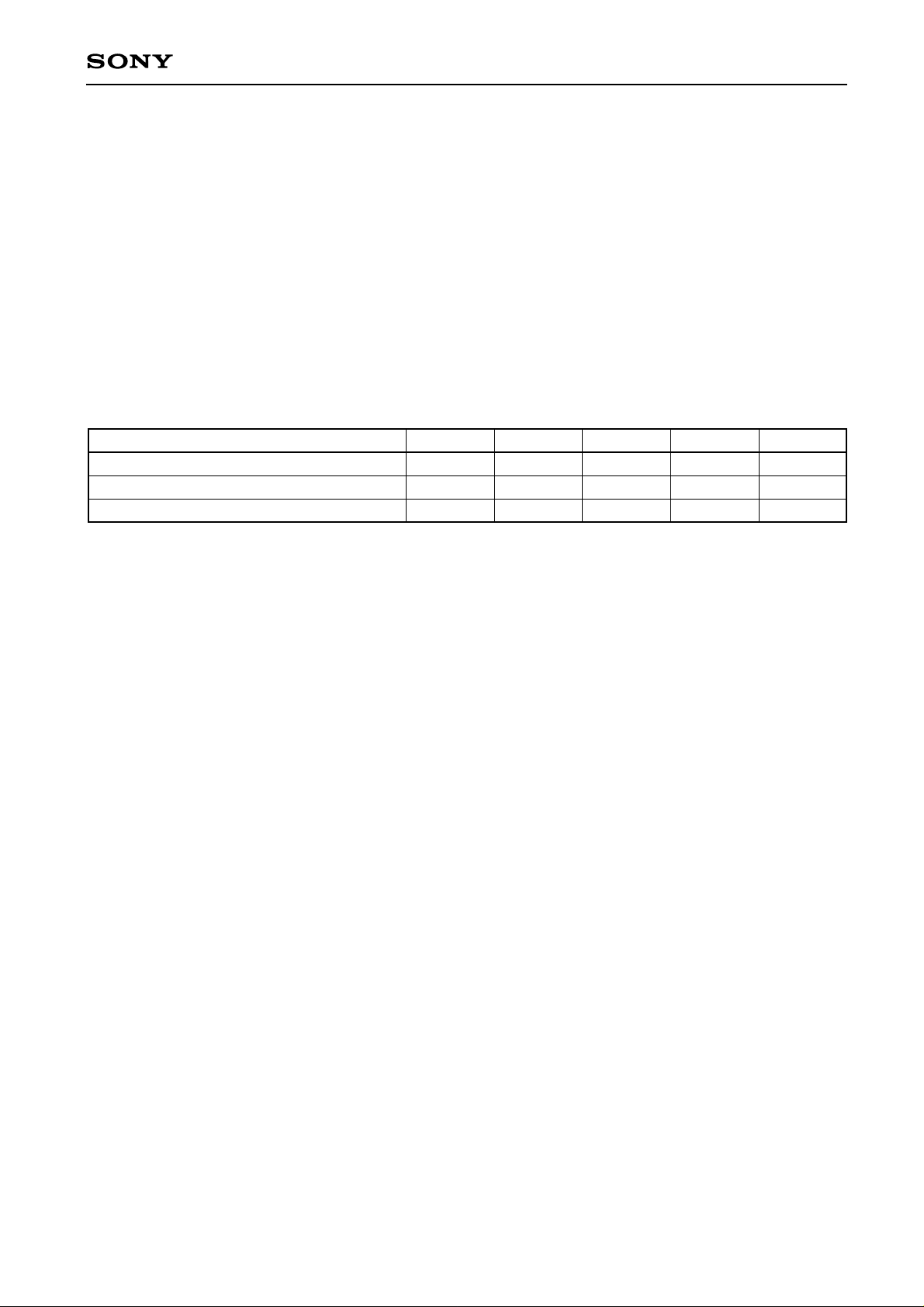
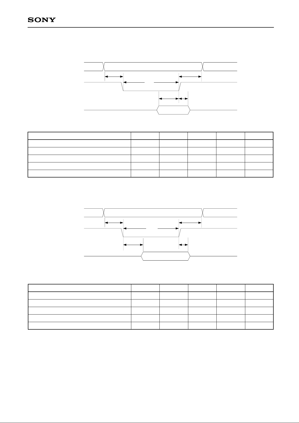
1. Sub CPU Interface
(1) Read
A0
Thar
XCS
Trrl
XRD
D7-0
Tsar
Tdrd
Tfrd
Item Symbol Min. Typ. Max. Unit
Address setup time (for XCS & XRD ↓) Tsar 30 (70) ns
Address hold time (for XCS & XRD ↑) Thar 20 (50) ns
Data delay time (for XCS & XRD↓) Tdrd 60 (100) ns
Data float time (for XCS & XRD ↑) Tfrd 0 15 (25) ns
Low level XRD pulse width Trrl 100 (150) ns
Note) "&" indicates "AND".
(2) Write
A0
XCS
Twwl
XWR
Thaw
D7-0
Tsaw
Tsdw
Thdw
Item Symbol Min. Typ. Max. Unit
Address setup time (for XCS & XWR ↓) Tsaw 30 (70) ns
Address hold time (for XCS & XWR ↑) Thaw 20 (50) ns
Data setup time (for XCS & XWR ↓) Tsdw 40 (70) ns
Data hold time (for XCS & XWR ↑) Thdw 10 (30) ns
Low level XWR pulse width Twwl 50 (80) ns
—9—

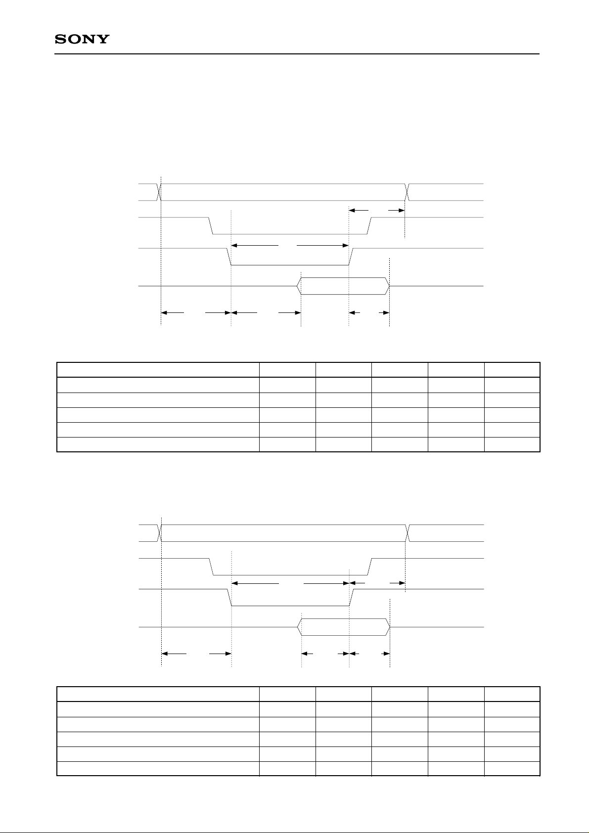
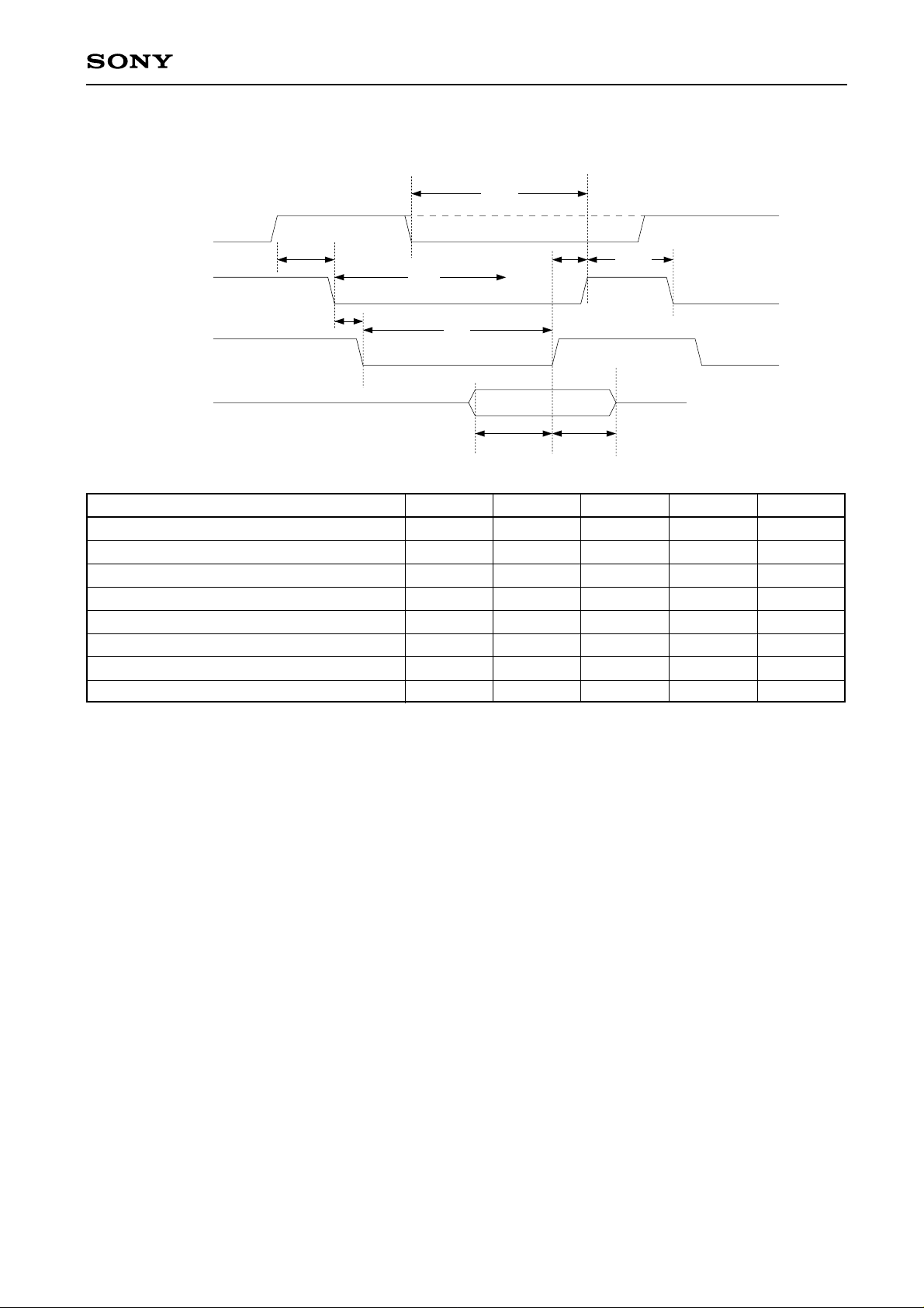
2. CD DSP Interface
BCKRED='H'
BCLK
DATA
LRCK
Tbck
Tsb1 Thb1
CXD1803AQ/AR
Tbck
C2PO
BCKRED='L'
BCLK
DATA
LRCK
C2PO
Tbck
Tsb1 Thb1
Thb2
Tbck
Thb2
Tsb2
Tsb2
Item Symbol Min. Typ. Max. Unit
BCLK frequency Fbck 11.3 MHz
BCLK pulse width Tbck 88 ns
DATA setup time (for BCLK) Tsb1 20 ns
DATA hold time (for BCLK) Thb1 20 ns
LRCK, C2PO setup time (for BCLK) Tsb2 20 ns
LRCK, C2PO hold time (for BCLK) Thb2 20 ns
—10—
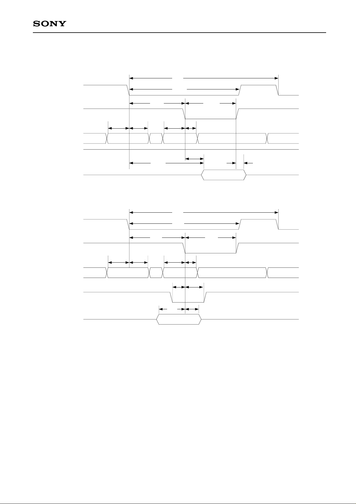
3. DRAM Interface
(1) Read
CXD1803AQ/AR
Trc
XRAS
XCAS
MA9-0
XMWR
MDB7-0, P
(2) Write
XRAS
XCAS
Tras
Trcd Tcas
Tasr
Tasr Trah Tasc Tcah
Trah Tasc Tcah
Row Column
Tcdd
Trdd
Trc
Tras
Trcd Tcas
Tcdh
'H'
MA9-0
XMWR
MDB7-0, P
Row Column
Twcs Twch
Tds
Tdh
—11—
CXD1803AQ/AR
Item Symbol Min. Typ. Max. Unit
Random read/write cycle time Trc 4Tw ns
RAS pulse width Tras 2Tw ns
RAS CAS delay time Trcd Tw ns
CAS pulse width Tcas Tw ns
Row address setup time Tasr 10 ns
Row address hold time Trah 20 ns
Column address setup time Tasc 0 ns
Column address hold time Tcah 20 ns
Delay time from RAS Trdd 2Tw-20 ns
Delay time from CAS Tcdd Tw-20 ns
Hold time from CAS Tcdh 0 ns
Write command setup time Twcs 10 ns
Write command hold time Twcs 20 ns
Data output setup time Tds Tw ns
Data output hold time Tds Tw ns
—12—
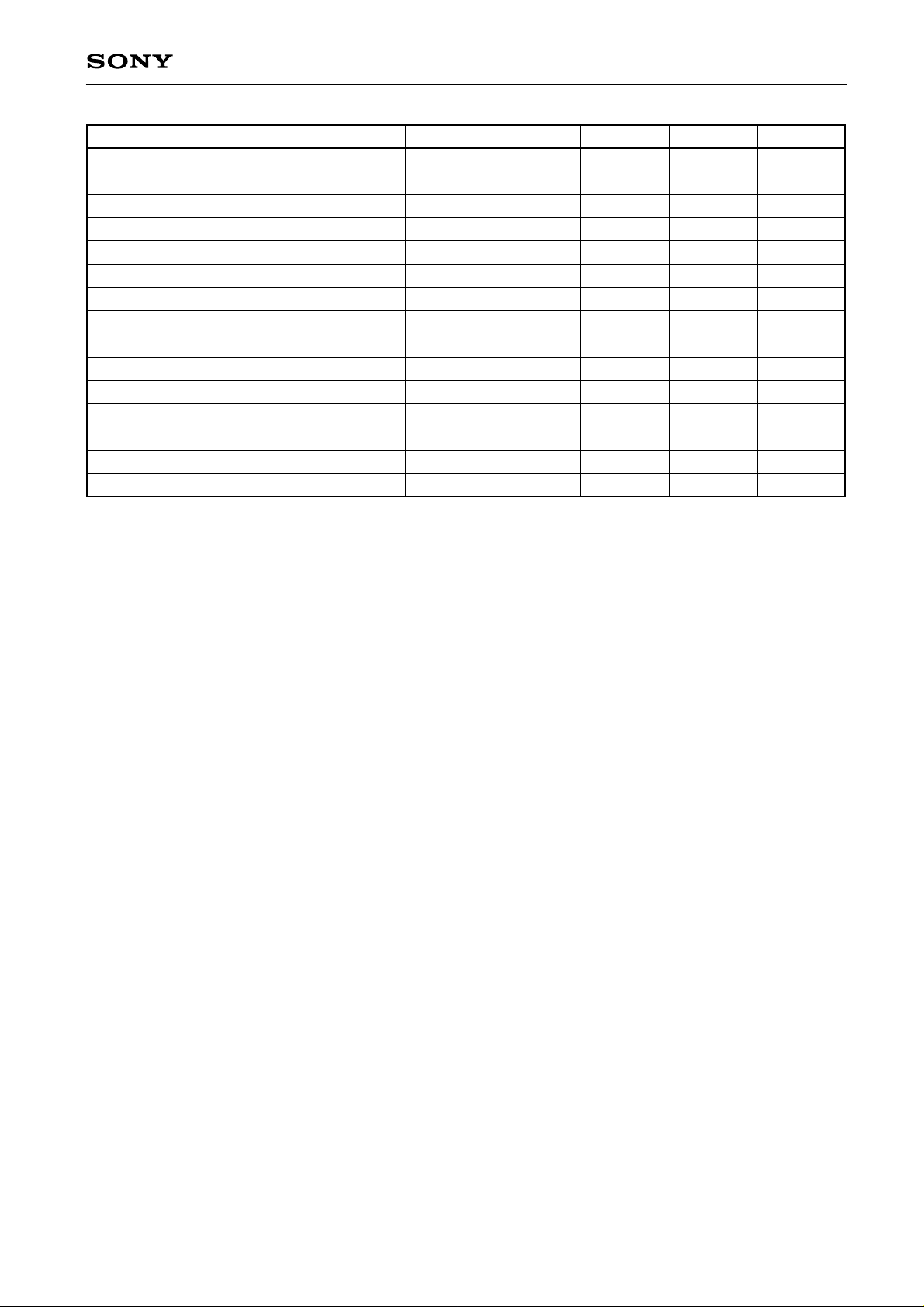
4. SRAM Interface
(1) Read
MA16-0
CXD1803AQ/AR
XMOE
MDB7-0,P
Taso
Trrl
Tsdo Thod
Thoa
XMWR='H'
Item Symbol Min. Typ. Max. Unit
Address setup time (for XMOE ↓) Tsao Tw-30 ns
Address hold time (for XMOE ↑) Thoa Tw-10 ns
Data setup time (for XMOE ↑) Tsdo 50 (100) ns
Data hold time (for XMOE ↑) Thod 10 (20) ns
Low level XMOE pulse width Trrl 2Tw ns
(2) Write
MA16-0
XMWR
MDB7-0,P
Tsaw
Twwl
Tdwd Tfwd
Thwa
XMOE='H'
Item Symbol Min. Typ. Max. Unit
Address setup time (for XMWR ↓) Tsaw Tw-30 ns
Address hold time (for XMWR ↑) Thwa Tw-10 ns
Data delay time (for XMWR ↓) Tdwd 10 ns
Data float time (for XMWR ↑) Tfwd 10 ns
Low level XMMR pulse width Twwl 2Tw ns
—13—
5. SCSI Controller Interface
(1) Read
SDRQ
CXD1803AQ/AR
Tsdq
XSAC
XSRD
SD7 to 0
Tdaw
Tdda
Tdar
Twwl
Trrl
Tsdr Thdr
Tasc
Item Symbol Min. Typ. Max. Unit
XSAC fall time (for SDRQ ↑) Tdda 5×Tw ns
XSRD delay time (for XSAC ↓) Tdaw 0 ns
XSAC delay time (for XSRD ↑) Tdar Tw ns
Data setup time (for XSRD ↓) Tsdr 20 (60) ns
Data hold time (for XSRD ↑) Thdr 10 (30) ns
Low level XSRD pulse width Trrl T1 ns
SDRQ setup time (for XSAC ↑) Tsdq 15 (30) ns
XSAC fall time (for XSAC ↑) Tsac Tw ns
—14—
 Loading...