

Sony CXD1267AN Datasheet

CCD Vertical Clock Driver
Description
The CXD1267AN is a vertical clock driver for CCD
image sensors. This IC is the successor of the
CXD1250N with attractive features.
Power consumption is reduced approximately 30%
for the CXD1267AN version.
Features
1) Substrate voltage (Vsub) generator is built-in.
• Variable Vsub in the range of 4.0V to 18.5V.
• Reduction of peripheral parts saves space.
2) Only two power supplies (+15V and –8.5V) are
needed.
3) 3.3V clock interface is acceptable.
4) 20-pin SSOP package is used.
5) Low power consumption
90mW (CXD1267N)
62mW (CXD1267AN)
approximately 30% reduction
CXD1267AN
20 pin SSOP (Plastic)
Appllications
CCD cameras
Structure
CMOS
Absolute Maximum Ratings (Ta = 25°C)
• Supply voltage VL 0 to –10 V
• Supply voltage VH VL – 0.3 to 2VL + 35 V
• Supply voltage VM VL – 0.3 to 3.0 V
• Input voltage VI VL – 0.3 to VH + 0.3 V
• Output voltage (V2, V4) MVφ VL – 0.3 to VM + 0.3 V
• Output voltage (V1, V3) HVφ VL – 0.3 to VH + 0.3 V
• Output voltage (VSHT) HHVφ VL – 0.3 to VH + 0.3 V
• Operational amplifier output current
IDCOUT ±5 mA
• Operating temperature Topr –25 to +85 °C
• Storage temperature Tstg –40 to +125 °C
Recommended Operating Conditions
• Supply voltage VH 14.5 to 15.5 V
• Supply voltage VM 0V
•Supply voltage VL –6.0 to –9.0 V
• Input voltage (except for pin 3)
VI 0 to 6.0 V
• Operational amplifier input voltage
VIOP 1.0 to 4.5 V
• Operating temperature Topr –20 to +75 °C
Sony reserves the right to change products and specifications without prior notice. This information does not convey any license by
any implication or otherwise under any patents or other right. Application circuits shown, if any, are typical examples illustrating the
operation of the devices. Sony cannot assume responsibility for any problems arising out of the use of these circuits.
– 1 –
E94X38-PK
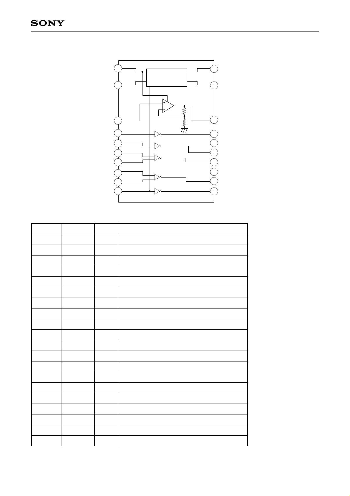
Block Diagram and Pin Configuration (Top View)
CXD1267AN
Pin Description
Pin No.
Symbol I/O Description
10
1
2
3
4
5
6
7
8
9
CPP3
V
H
DCIN
XSHT
XV2
XV1
XSG1
XV3
XSG2
XV4
Charge Pump
CPP1
CPP2
DCOUT
VSHT
V
Vφ2
Vφ1
VM
Vφ3
Vφ4
20
19
18
17
L
16
15
14
13
12
11
1
2
3
4
5
6
7
8
9
10
11
12
13
14
15
16
17
CPP3
VH
DCIN
XSHT
XV2
XV1
XSG1
XV3
XSG2
XV4
Vφ4
Vφ3
VM
Vφ1
Vφ2
VL
VSHT
O
—
O
O
—
O
O
—
O
Charge pump
Power supply (15V)
I
Operational amplifier input
I
Output control (VSHT)
I
Output control (Vφ2)
I
Output control (Vφ1)
I
Output control (Vφ1)
I
Output control (Vφ3)
I
Output control (Vφ3)
I
Output control (Vφ4)
High-voltage output (2 levels: VM, VL)
High-voltage output (3 levels: VH, VM, VL)
GND
High-voltage output (3 levels: VH, VM, VL)
High-voltage output (2 levels: VM, VL)
Power supply (–8.5V)
High-voltage output (2 levels: VH, VL)
18
19
20
DCOUT
CPP2
CPP1
O
—
—
Operational amplifier output
Charge pump
Charge pump
– 2 –

Truth Table
CXD1267AN
Input
XV1, 3
H
H
XSG1, 2 XV2, 4 XSHT
L
L
L
L
H
H
X
X
X
X
X
X
X
X
X
X
X
X
L
H
X
X
Electrical Characteristics
DC Characteristics
Item
High level input voltage
Low level input voltage
Output
Vφ1, 3 Vφ2, 4
X
X
X
X
X
X
L
H
VH
Z
VM
VL
X
X
X
X
X
X
X
X
VM
VL
X
X
VSHT
X
X
X
X
X
X
VH
VL
X: Don't care
Z: High impedance
(Unless otherwise specified, Ta = 25°C, VH = 15V, VM = GND, VL = –8.5V)
Symbol Condition Min. Typ. Max. Unit
VIH
VIL
2.3
—
—
—
—
1.3
V
V
High level output voltage
Middle level output voltage
Middle level output voltage
Low level output voltage
VOH
VOM1
VOM2
VOL
IO = –20µA
IO = 20µA
IO = –20µA
IO = 20µA
14.9
—
–0.1
—
15.0
0.0
0.0
–8.5
—
0.1
—
–8.4
–1 ≤ ICPP3 ≤ 0mA
Charge pump output voltage
VCPP3
IDCOUT = 0mA, Ta = –20 to 75°C
20
—
—
VIOP = 4.5V
Input current
Operating supply current
Operating supply current
Output current
Output current
Output current
Output current
Output current
Output current
Operational amplifier gain
Gain error
II
IH
IL
IOL
IOM1
IOM2
IOH
IOSL
IOSH
G
∆G
VI = VL to 5V
∗1
∗1
Vφ1 to 4 = –8.0V
Vφ1 to 4 = –0.5V
Vφ1, 3 = 0.5V
Vφ1, 3 = 14.5V
VSHT = –8.0V
VSHT = 14.5V
IDCOUT = –200/+100µA
Ta = –20 to 75°C
∗2
IDCOUT = –200/+100µA
–1.0
—
–6.0
25
—
9
—
12
—
—
–3
0.0
1.4
–5.0
—
—
—
—
—
—
× 4.40
—
1.0
2.0
—
—
–10
—
–12
—
–7
—
+3
VIOP = 1.0 to 4.5V
∗1
See Measurement Circuit. Shutter speed: 1/10000.
∗2
See Operational Amplifier Gain Characteristic.
Note) Current directions: + indicates the direction flowing to IC; – indicates the direction flowing from IC
V
V
V
V
V
µA
mA
mA
mA
mA
mA
mA
mA
mA
%
– 3 –
 Loading...