

Sony CXD1261AR Datasheet

Description
The CXD1261AR is an IC which generates the
sync signals and timing signals required for a
camera system that uses the monochrome CCD
image sensor (760H) such as the ICX038/039 and
ICX058/059.
Features
• Compatible with monochrome (EIA/CCIR) systems
• Built-in electronic shutter function
• Built-in driver for the horizontal (H) clock
• Built-in SG and TG functions
Applications
CCD camera systems
Structure
Silicon gate CMOS
Absolute Maximum Ratings (Ta = 25°C, Vss = 0V)
• Supply voltage VDD VSS – 0.5 to +7.0 V
• Input voltage VI Vss – 0.5 to VDD + 0.5 V
• Output voltage VO Vss – 0.5 to VDD + 0.5 V
• Operating temperature Topr –20 to +75 °C
• Storage temperature Tstg –55 to +150 °C
Recommended Operating Conditions
• Supply voltage VDD 5.0 ± 0.25 V
• Operating temperature Topr –20 to +75 °C
– 1 –
CXD1261AR
E95735B7Y-PS
Sync Signal, Timing Signal Generator for CCD Cameras
Sony reserves the right to change products and specifications without prior notice. This information does not convey any license by
any implication or otherwise under any patents or other right. Application circuits shown, if any, are typical examples illustrating the
operation of the devices. Sony cannot assume responsibility for any problems arising out of the use of these circuits.
64 pin LQFP (PIastic)
– 2 –
CXD1261AR
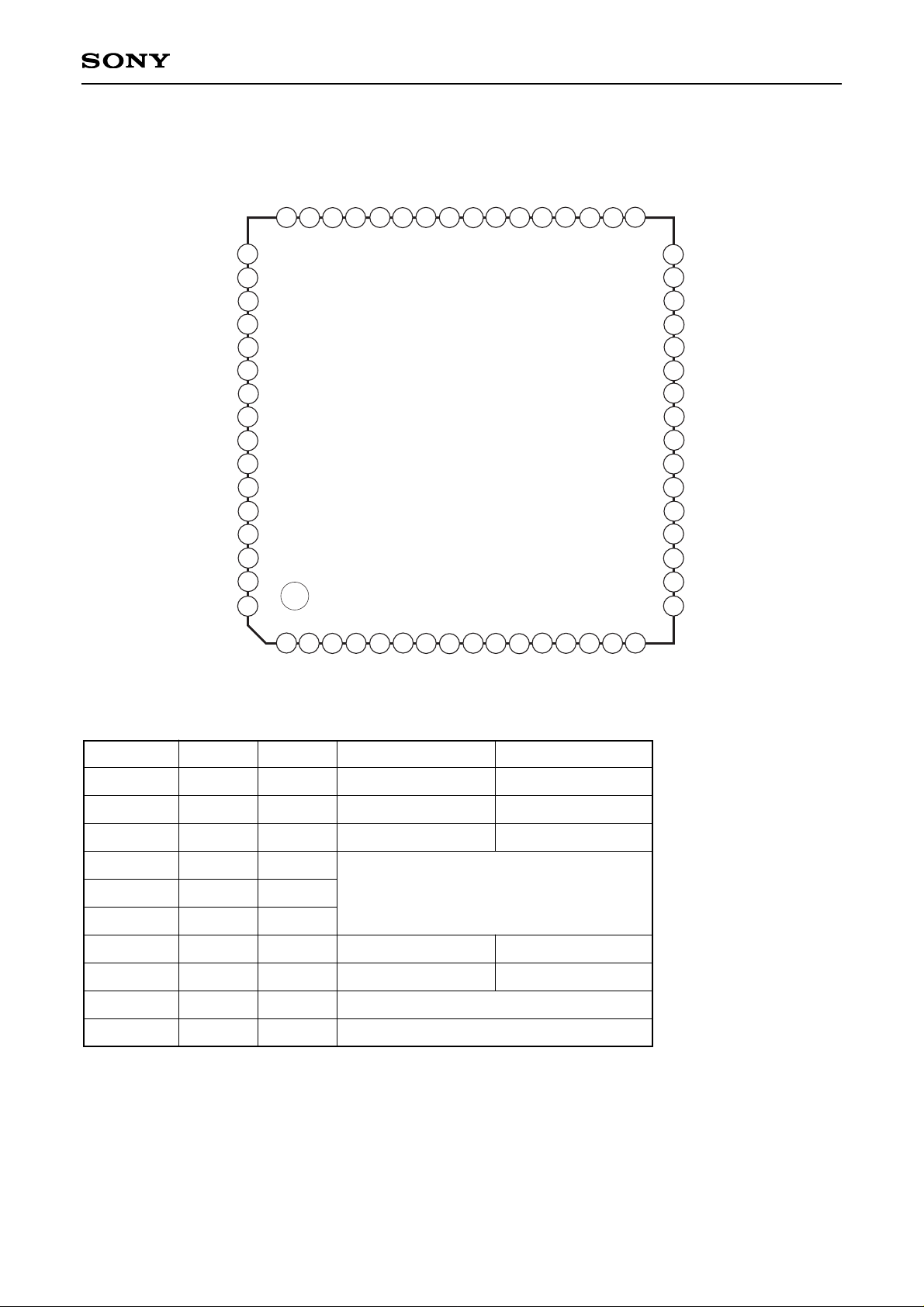
Pin Configuration
17
18
19
20
21
22
23
24
25
26
27
28
29
30
31
32
49
50
51
52
53
54
55
56
57
58
59
60
63
64
61
62
2
3
4
5
6
7
8
9
10
11
12
13
14
15
16
1
40
39
38
37
36
35
34
33
41
42
43
44
45
46
47
48
VSS
XV4
XSG2
XV3
XSG1
XV1
XV2
XSUB
V
DD
RG
V
SS
TST3
H2
TST2
H1
V
DD
VR/FLD
HTSG
V
DD
EXT
V
SS
TST10
TST11
V
DD
TST12
TST13
V
SS
TST14
TST15
TST16
CBLK
SYNC
HD
VD
CL
D1
D2
TST1
TRIG
V
SS
OSCI
OSCO
CKIN
ENB
ED0
ED1
ED2
PS
HR
V
DD
TST9
PBLK
CLP4
CLP3
CLP2
CLP1
V
SS
TST8
TST7
TST6
TST5
TST4
SHD
SHP
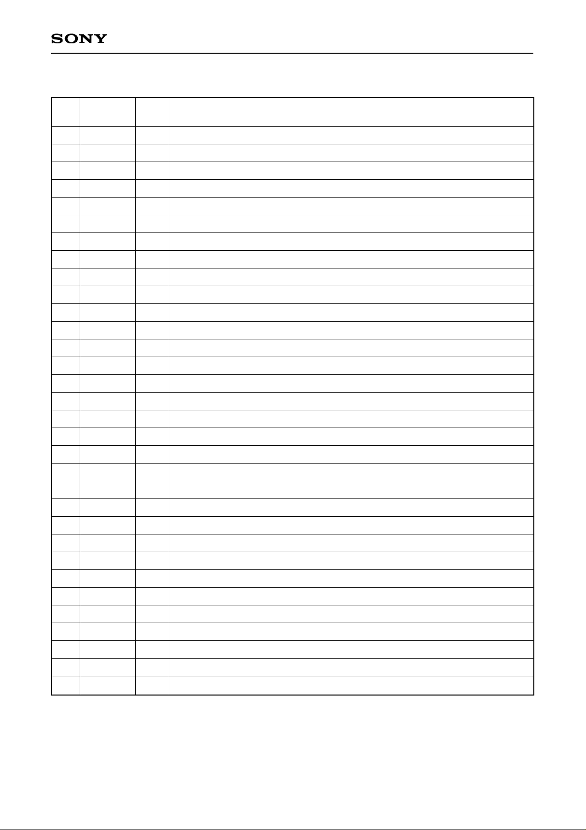
Mode name Pin No. PRESET L
H
D1
D2
ENB
ED0
ED1
ED2
PS
EXT
TST1
TST13
4
5
12
13
14
15
16
52
6
58
L
L
H
H
H
H
H
L
—
—
EIA CCIR
Field readout Frame readout
Normal Shutter
Shutter speed
Serial input Parallel input
Internal External
Normally High
Normally Low
Note) Normally open for TST except as shown in the above table.
∗
During frame accumulation (readout), low-speed shutter does not operate normally.
∗
∗
– 3 –
CXD1261AR
Pin
No.
Symbol
1
2
3
4
5
6
7
8
9
10
11
12
13
14
15
16
17
18
19
20
21
22
23
24
25
26
27
28
29
30
31
32
I/O Description
HD
VD
CL
D1
D2
TST1
TRIG
VSS
OSCI
OSCO
CKIN
ENB
ED0
ED1
ED2
PS
VDD
H1
TST2
H2
TST3
VSS
RG
VDD
XSUB
XV2
XV1
XSG1
XV3
XSG2
XV4
VSS
O
O
O
I
I
I
I
—
I
O
I
I
I
I
I
I
—
O
I
O
I
—
O
—
O
O
O
O
O
O
O
—
Horizontal drive pulse
Vertical drive pulse
CKIN 2 frequency divided output (EIA: 14.318MHz, CCIR: 14.1875MHz)
Mode switching; low: EIA; high: CCIR (with pull-down resistor)
Mode switching; low: field readout; high: frame readout∗(with pull-down resistor)
Test input, fixed to high
Shutter speed setting pulse (with pull-up resistor)
GND
Oscillating cell input
Oscillating cell output
Clock input (EIA: 28.636MHz, CCIR: 28.375MHz)
Shutter switching; low: normal; high: shutter (with pull-up resistor)
Shutter speed control (with pull-up resistor)
Shutter speed control (with pull-up resistor)
Shutter speed control (with pull-up resistor)
Shutter speed setting method switching; low: serial; high: parallel (with pull-up resistor)
Power supply
Horizontal register drive clock
Test input, normally open (with pull-down resistor)
Horizontal register drive clock
Test input, normally open (with pull-down resistor)
GND
Reset gate pulse
Power supply
Discharge pulse
Vertical register drive clock
Vertical register drive clock
Sensor charge readout pulse
Vertical register drive clock
Sensor charge readout pulse
Vertical register drive clock
GND
Pin Description
∗
The CCD image sensor characteristics are guaranteed for field accumulation operation.
– 4 –
CXD1261AR
33
34
35
36
37
38
39
40
41
42
43
44
45
46
47
48
49
50
51
52
53
54
55
56
57
58
59
60
61
62
63
64
SHP
SHD
TST4
TST5
TST6
TST7
TST8
VSS
CLP1
CLP2
CLP3
CLP4
PBLK
TST9
VDD
HR
VR/FLD
HTSG
VDD
EXT
VSS
TST10
TST11
VDD
TST12
TST13
VSS
TST14
TST15
TST16
CBLK
SYNC
O
O
O
O
O
O
O
—
O
O
O
O
O
O
—
I
I
I
—
I
—
I
O
—
O
I
—
O
O
O
O
O
Precharge level sample-and-hold pulse
Data sample-and-hold pulse
Test output, normally open
Test output, normally open
Test output, normally open
Test output, normally open
Test output, normally open
GND
Clamp pulse
Clamp pulse
Clamp pulse
Clamp pulse
Blanking cleaning pulse
Test output, normally open
Power supply
H reset pulse
V reset pulse (FLD output when EXT = low)
HTSG input; low: XSG1, 2 on; high: off (valid only when EXT = low)
Fixed to low when EXT = high
Power supply
Sync mode switching; low: internal; high: external sync (with pull-down resistor)
GND
Test input, normally open (with pull-down resistor)
Test output, normally open
Power supply
Test output, normally open
Test input, fixed to low
GND
Test output, normally open
Test output, normally open
Test output, normally open
Composite blanking pulse
Composite sync pulse
Pin
No.
Symbol I/O Description
– 5 –
CXD1261AR
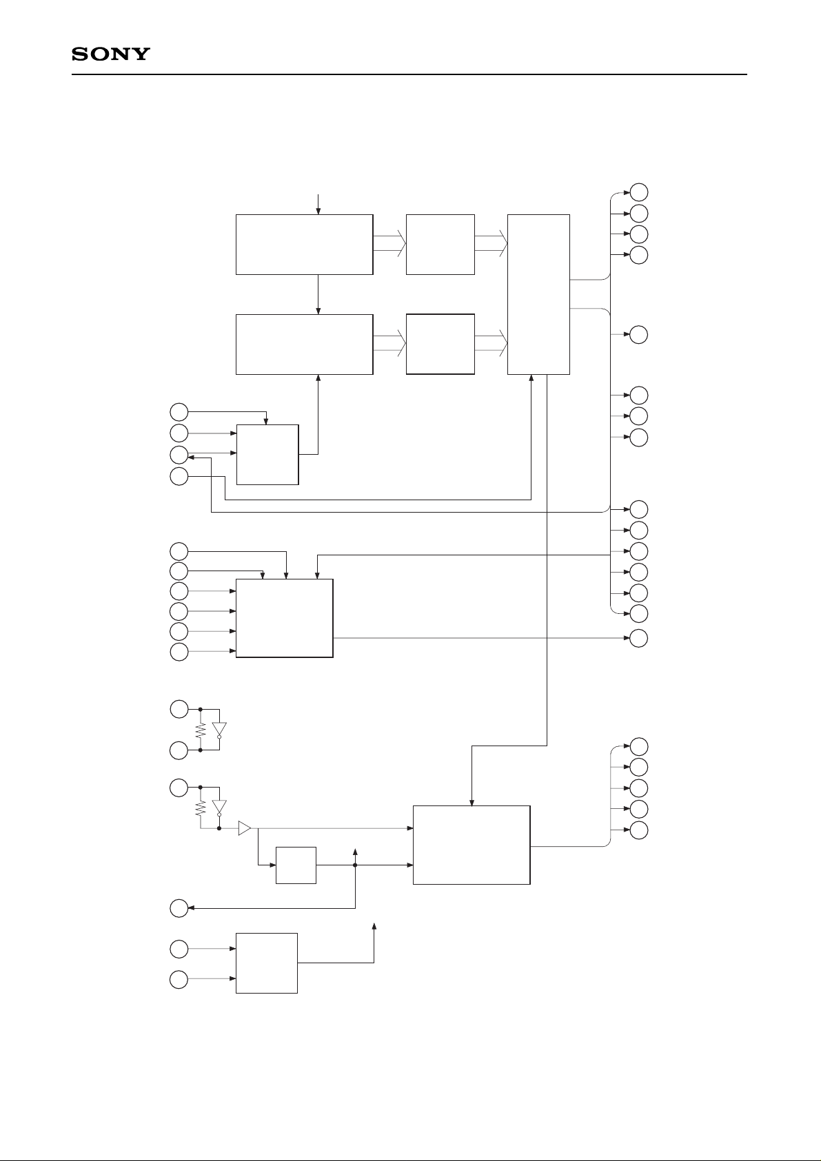
Block Diagram
18
20
23
25
26
27
28
29
30
31
33
41
42
43
45
63
48
49
50
52
7
12
13
14
15
16
9
10
11
3
4
5
2
64
1
CL
H Counter
1/910 or 1/908
V Counter
1/525 or 1/625
Decoder
Decoder
Pulse
Generator
Reset
Generator
HTSG
FLD
XSUB
Shutter Control
1/2
High-speed Pulse
Generator
Mode
Setting
CL
RG
H1
H2
SHP
XV3
XV4
XSG1
XSG2
XSUB
XV1
XV2
CLP3
CLP1
CLP2
PBLK
HD
VD
CBLK
SYNC
VR/FLD
HTSG
EXT
HR
ED0
ED1
ENB
PS
ED2
TRIG
OSCI
OSCO
CKIN
CL
D1
D2
34
SHD
– 6 –
CXD1261AR
Electrical Characteristics
1) DC characteristics (VDD = 5V ± 0.25V, Topr = –20 to +75°C)
2) I/O pin capacitance (VDD = V1 = 0V, fM = 1MHz)
Item
Symbol Conditions Min. Typ. Max. Unit
Supply voltage
Input voltage
Output voltage 1
∗
1
Output voltage 2
∗
2
Output voltage 3
∗
3
Output voltage 4
∗
4
Feedback resistor
Pull-up resistor
Pull-down resistor
VDD
VIH1
VIL1
VOH1
VOL1
VOH2
VOL2
VOH3
VOL3
VOH4
VOL4
RFB
RPU
RPD
IOH = –2mA
IOL = 4mA
IOH = –4mA
IOL = 8mA
IOH = –8mA
IOL = 8mA
IOH = –2mA
IOL = 2mA
VIN = VSS or VDD
VIL = 0V
VIH = VDD
4.75
0.7VDD
VDD – 0.5
VDD – 0.5
VDD – 0.5
VDD/2
500K
40K
40K
5.0
2M
100K
100K
5.25
0.3VDD
0.4
0.4
0.4
VDD/2
5M
250K
250K
V
V
V
V
V
V
V
V
V
V
V
Ω
Ω
Ω
Item
Symbol Min. Typ. Max. Unit
Input pin capacitance
Output pin capacitance
Input/output pin capacitance
CIN
COUT
CI/O
9
11
11
pF
pF
pF
Note)
∗1
CLP1, CLP2, CLP3, CLP4, PBLK, CBLK, SYNC, VR, HD, VD, XSUB, XSG1, XSG2, XV1, XV2,
XV3, XV4
∗2
CL, RG, SHP, SHD
∗3
H1, H2
∗4
OSCO
– 7 –
CXD1261AR
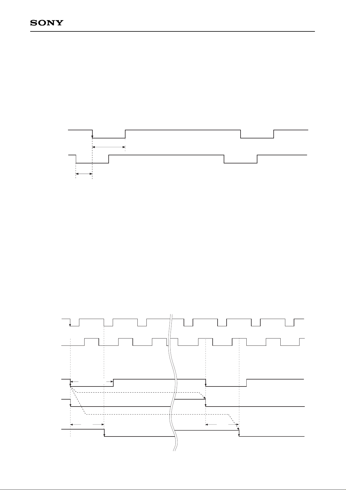
External Reset Description
H Reset (HR)
The reset is performed at the first falling edge of the reset pulse that was input; resets are not performed at
subsequent edges as long as they do not deviate by two clock pulses (0.14µs) or more.
The minimum reset pulse width is 0.35µs. In addition, HD immediately after a reset can not be guaranteed.
The position at which the reset is performed is 2.31µs advanced after the H reset input.
H reset input
HD output
0.35µs or more
2.31µs
V Reset (VR)
The falling edge of V reset pulse that was input is field identified by the phase difference with the internal signal
(field judge pulse) defined by the falling edge of HD. And VD is reset in phase with V reset pulse.
When field judge pulse is low and V reset pulse falls,
EIA: VD falling edge after 262.5H is the relation between HD and VD of EVEN field.
CCIR: VD falling edge after 313.5H is the relation between HD and VD of ODD field.
Also, when field judge pulse is high and V reset pulse falls,
EIA: VD falling edge after 262.5H is the relation between HD and VD of ODD field.
CCIR: VD falling edge after 313.5H is the relation between HD and VD of EVEN field.
The minimum reset pulse width is 64µs.
HD output
Field
judge
pulse
VR input
VD output
(EIA)
VD output
(CCIR)
1HD
1 2 3
262
(312)
263
(313)
264
(314)
The value without ( ) is for EIA
The value in ( ) is for CCIR
1HD
Note: For CCIR, VD output is delayed 1HD in relation to VR input.
VD timing is genarated after
262.5H with this VR timing
VD timing is genarated after
313.5H with this VR timing
64µs or more
 Loading...