

Sony CXD1198AQ Datasheet

—1—
E92632A78-TE
Sony reserves the right to change products and specifications without prior notice. This information does not convey any license by
any implication or otherwise under any patents or other right. Application circuits shown, if any, are typical examples illustrating the
operation of the devices. Sony cannot assume responsibility for any problems arising out of the use of these circuits.
Absolute Maximum Ratings (Ta=25 °C)
• Supply voltage VCC –0.5 to +7.0 V
• Input voltage VI –0.5 to VDD +0.5 V
• Output voltage VO –0.5 to VDD +0.5 V
• Operating temperature Topr –20 to +75 °C
• Storage temperature Tstg –55 to +150 °C
Recommended Operating Conditions
• Supply voltage VDD 5.0±0.5 V
• Operating temperature Topr –20 to +75 °C
Description
The CXD1198AQ is a CD-ROM subcode decoder
LSI.
Features
• Real time error correction of subcodes
• Connection possible with DRAM up to 1 MB as
buffer memory
• Automatic generation of sync patterns
• Error pointer buffering function (separated mode,
mixed mode)
• 4 MB/s maximum rate for transferring data with
SCSI control LSI
Applications
CD-ROM drives
Structure
Silicon gate CMOS IC
CD-ROM Subcode Decoder
100 pin QFP (Plastic)
CXD1198AQ
For the availability of this product, please contact the sales office.

—2—
CXD1198AQ
Block Diagram
DDB0-7
DDBP
XDAC
DDRQ
XDWR
XDRD
XDCA
D
r
i
v
e
I
n
t
e
r
f
a
c
e
C
o
n
t
r
o
l
DMA
Refresh
Control
DMA Controller
(priority resolver, sequencer)
30
27
26
31-39,41
18-25
52
71
72
55
62
67
66
64
63
68
69
70
50
51
46
1/2
48
47
XTL2
XTL1
49
14
1,2,5-10
95-100
121113
17
16
42
43
44
45
77
93
94
80
75
76
89
91
92
81
88
H
O
S
T
I
n
t
e
r
f
a
c
e
C
o
n
t
r
o
l
HMDS
HINT
HINP
HBD0-7
XHAC/
SDRQ
HDRQ/
XSAC
XHWR
XHRD
XHCS
HA0,1
XSRS
XHRS
HCLK
INTP
INT
XCS
XRD
XWR
A0-5
DB0-7
XCRS
XRST
CPU Interface, DMA Control
RAM
De-Interleave
Subcode
DMA
Control
Subcode
Interface
Control
S/P
Error
Corrector
EXCK
SBSO
SCOR
WFCK
XDRS
DA0,1
Drive
DMA
Control
Pointer
S/P
Sync.
Pattern
Pointer
DMA
Control
HOST
DMA
Control
FIFO
(10bytes x 2)
Reset
Control
Internal
Clock
XRAS
XCAS
XWE
BA0-9
BDB0-7
—3—
CXD1198AQ
Pin Description
Pin No. Symbol I/O Description
1
2
3
4
5
6
7
8
9
10
11
12
13
14
15
16
17
18
19
20
21
22
23
24
25
26
27
28
29
30
31
32
33
34
DB0
DB1
VDD
VSS
DB2
DB3
DB4
DB5
DB6
DB7
XRD
XWR
XCS
XCRS
VSS
INTP
INT
BDB0
BDB1
BDB2
BDB3
BDB4
BDB5
BDB6
BDB7
XWE
XCAS
VDD
VSS
XRAS
BA0
BA1
BA2
BA3
I/O
I/O
I/O
I/O
I/O
I/O
I/O
I/O
I
I
I
O
I
O
I/O
I/O
I/O
I/O
I/O
I/O
I/O
I/O
O
O
O
O
O
O
O
CPU data bus
CPU data bus
Power supply (+5 V)
GND
CPU data bus
CPU data bus
CPU data bus
CPU data bus
CPU data bus
CPU data bus
Register read strobe negative logic signal in this IC
Register write strobe negative logic signal in this IC
Chip select signal to this IC
Reset negative logic signal to CPU
GND
INT signal polarity control input signal
Interrupt request signal to CPU
Buffer memory data bus
Buffer memory data bus
Buffer memory data bus
Buffer memory data bus
Buffer memory data bus
Buffer memory data bus
Buffer memory data bus
Buffer memory data bus
Strobe negative logic signal for writing in buffer memory
Strobe negative logic signal for column address in buffer memory
Power supply (+5 V)
GND
Strobe negative logic signal for row address in buffer memory
Buffer memory address
Buffer memory address
Buffer memory address
Buffer memory address

—4—
CXD1198AQ
Pin No. Symbol I/O Description
35
36
37
38
39
40
41
42
43
44
45
46
47
48
49
50
51
52
53
54
55
56
57
58
59
60
61
62
63
64
65
66
67
BA4
BA5
BA6
BA7
BA8
VSS
BA9
EXCK
SBSI
SBSY
WFCK
XTL2
XTL1
HCLK
XRST
XSRS
XHRS
HMDS
VDD
VSS
HDB7
HDB6
HDB5
HDB4
HDB3
HDB2
HDB1
HDB0
XHRD
XHWR
VSS
HDRQ
/XSAC
XHAC
/SDRQ
O
O
O
O
O
O
O
I
I
I
O
I
O
I
I
O
I
I/O
I/O
I/O
I/O
I/O
I/O
I/O
I/O
I/O
I/O
O
I
Buffer memory address
Buffer memory address
Buffer memory address
Buffer memory address
Buffer memory address
GND
Buffer memory address
Subcode data readout clock output signal to the CXD2500
Subcode data input signal from the CXD2500
Subcode frame sync input signal from the CXD2500
Write frame clock input signal from the CXD2500
Crystal oscillator circuit output
Crystal oscillator circuit input
Crystal 1/2 frequency-divided clock output
Reset negative logic input signal
SCSI bus reset negative logic input signal
Reset negative logic output signal to host
Host mode select input signal
Power supply (+5 V)
GND
Host data bus
Host data bus
Host data bus
Host data bus
Host data bus
Host data bus
Host data bus
Host data bus
Data read strobe signal from host or to SCSI control IC
Data write strobe signal from host or to SCSI control IC
GND
Data request positive logic signal to host or DMA acknowledge negative
logic signal to SCSI control IC
DMA acknowledge negative logic signal from host or data request
positive logic signal from SCSI control IC
—5—
CXD1198AQ
Pin No. Symbol I/O Description
68
69
70
71
72
73
74
75
76
77
78
79
80
81
82
83
84
85
86
87
88
89
90
91
92
93
94
95
96
97
98
99
100
XHCS
HA0
HA1
HINT
HINP
NC1
NC2
XDAC
DDRQ
XDRS
VDD
VSS
DDBP
DDB7
DDB6
DDB5
DDB4
DDB3
DDB2
DDB1
DDB0
XDWR
VSS
XDRD
XDCS
DA1
DA0
A5
A4
A3
A2
A1
A0
I
I
I
O
I
O
O
O
I
O
I/O
I/O
I/O
I/O
I/O
I/O
I/O
I/O
I/O
O
O
O
O
O
I
I
I
I
I
I
Chip select input signal from host
Host address signal
Host address signal
Interrupt request signal to host
HINT signal polarity control input signal
No connection; leave open.
No connection; leave open.
DMA acknowledge negative logic signal to the CXD1186BQ
Data request positive logic signal from the CXD1186BQ
Reset negative logic signal to the CXD1186BQ
Power supply (+5 V)
GND
Error pointer bus connected with the CXD1186BQ
Data bus connected with the CXD1186BQ
Data bus connected with the CXD1186BQ
Data bus connected with the CXD1186BQ
Data bus connected with the CXD1186BQ
Data bus connected with the CXD1186BQ
Data bus connected with the CXD1186BQ
Data bus connected with the CXD1186BQ
Data bus connected with the CXD1186BQ
Host register write strobe negative logic signal to the CXD1186BQ
GND
Host register read strobe negative logic signal to the CXD1186BQ
Chip select negative logic signal for host register read/write to the
CXD1186BQ
Address signal to the CXD1186BQ
Address signal to the CXD1186BQ
CPU address signal
CPU address signal
CPU address signal
CPU address signal
CPU address signal
CPU address signal
—6—
CXD1198AQ
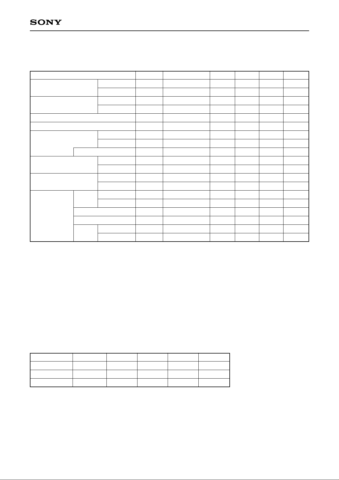
Electrical Characteristics
DC characteristics (VDD=5.0±0.5 V, VSS=0 V, Topr=–20 to +75 °C)
Item
TTL input voltage High level
Low level
CMOS input voltage High level
Low level
Input current of pull-up input
Input current of pull-down input
CMOS Schmitt High level
input voltage Low level
Hysteresis
Output voltage High level
Low level
Charge pump High level
output voltage Low level
Oscillation cell Input High level
voltage Low level
Logic threshold
Feedback resistance
Output High level
voltage Low level
Symbol
VIH1
VIL1
VIH2
VIL2
IIL
IIH
Vt+
Vt–
Vt+–Vt–
VOH1
VOL1
VOH2
VOL2
VIH3
VIL3
LVth
RFB
VOH3
VOL3
Conditions
VIL=0 V
VIH=VDD
IOH1=–2 mA
IOL1=4 mA
IOH2=–6 mA
IOL2=4 mA
VIN=VSS or VDD
IOH3=–3 mA
IOL3=3 mA
Min. Typ. Max. Unit
2.2 V
0.8 V
0.7VDD V
0.3VDD V
–40 –100 –240 µA
40 100 240 µA
0.8VDD V
0.2VDD V
0.6 V
VDD–0.8 V
0.4 V
VDD–0.8 V
0.4 V
0.7VDD V
0.3VDD V
VDD/2 V
250 k 1 M 2.5 M Ω
VDD/2 V
VDD/2 V
CMOS input pins : DDRQ, SBSY, SBSI, A5 to 0, XWR, XRD, XCS, INTP
CMOS Schmitt input pins : WFCK, XRST
Pull-up input pins : XHCS, HA1, HA0
PUll-down input pin : HMDS
Charge pump output pins : HINT, BA9 to 0
Oscillation cell input pin : XTL1
Oscillation cell output pin : XTL2
The characteristics for all other pins follow the TTL input and output voltage items. All bidirectional data buses
are pulled up by standard 25 kΩ resistance.
Input/output capacitance VDD=VI=0 V, f=1 MHz
Item
Input pin
Output pin
I/O pin
Symbol
CIN
COUT
CI/O
Min. Typ. Max.
9
11
11
Unit
pF
pF
pF
—7—
CXD1198AQ
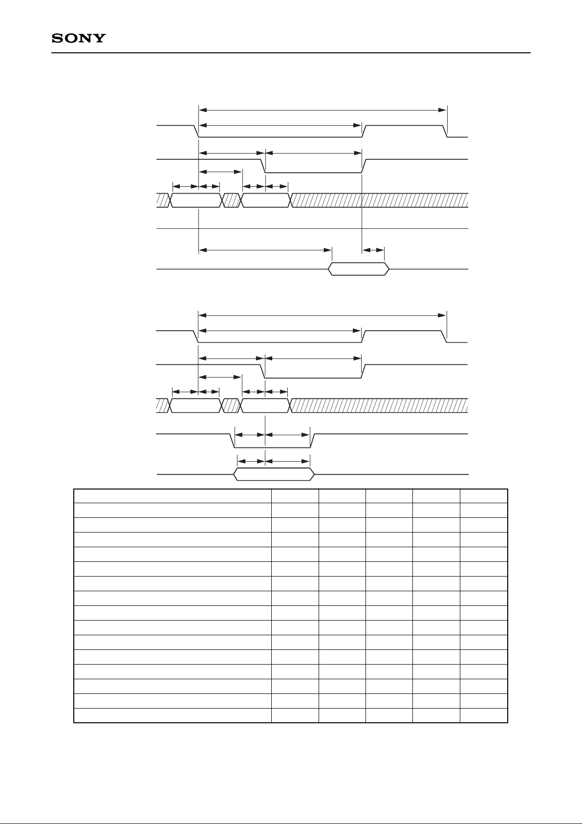
AC characteristics (Ta=–20 to +75 °C, VDD=5 V±10 %, output load=75 pF, f≤24 MHz)
1. CPU interface
(1) Read
(2) Write
A0 to 5
XCS
XRD
DB0 to 7
t
SRC
tHRC
tSRA
tDRD
tHRA
tFRD
tRRL
Item
Address setup time (vs. XRD↓)
Chip select setup time (vs. XRD↓)
Data delay time (vs. XRD↓)
Data float time (vs. XRD↑)
Chip select hold time (vs. XRD↑)
Address hold time (vs. XRD↑)
Low-level XRD pulse width
Symbol
tSRA
tSRC
tDRD
tFRD
tHRC
tHRA
tRRL
Min.
20
0
3
0
0
100
Typ. Max.
80
10
Unit
ns
ns
ns
ns
ns
ns
ns
A0 to 5
XCS
XWR
DB0 to 7
t
SCW
tWWL
tHWC
tHWA
tHWD
tSAW
tSDW
Item
Address setup time (vs. XWR↓)
Chip select setup time (vs. XWR↓)
Data setup time (vs. XWR↓)
Data hold time (vs. XWR↑)
Chip select hold time (vs. XWR↑)
Address hold time (vs. XWR↑)
Low-level XWR pulse width
Symbol
tSAW
tSCW
tSDW
tHWD
tHWC
tHWA
tWWL
Min.
20
0
40
10
0
0
50
Typ. Max. Unit
ns
ns
ns
ns
ns
ns
ns
—8—
CXD1198AQ
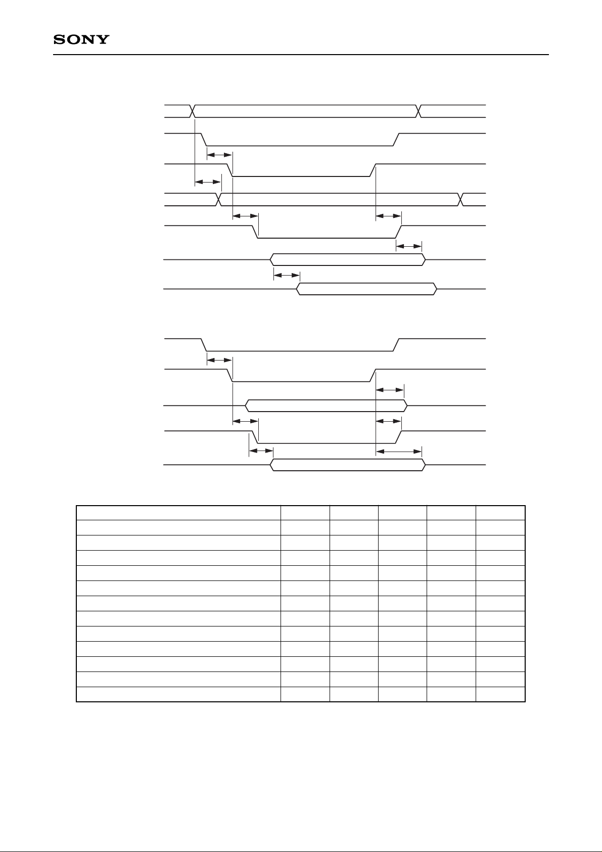
2. DRAM interface
(1) Read
(2) Write
tRC
tRAS
tRCD
tRAD
tASR tASC
tRDD
tCDH
tCAHtRAH
tCAS
ROW COLUMN
high
XRAS
XCAS
BA0 to 9
XWE
BB0 to 7
tRC
tRAS
tRCD
tRAD
tASR tASC
tWCS
tDS tDH
tWCH
tCAHtRAH
tCAS
ROW COLUMN
XRAS
XCAS
BA0 to 9
XWE
BB0 to 7
Item
Random read/write cycle time
RAS pulse width
RAS/CAS delay time
CAS pulse width
RAS/column address delay time
Row address setup time
Row address hold time
Column address setup time
Column address hold time
Delay time from RAS
Hold time from CAS
Write command setup time
Write command hold time
Data output setup time
Data output hold time
Symbol
tRC
tRAS
tRCD
tCAS
tRAD
tASR
tRAH
tASC
tCAH
tRDD
tCDH
tWCS
tWCH
tDS
tDH
Min.
2TW+5
TW+5
TW/2+5
10
TW/2
0
TW/2
0
10
20
10
20
Typ.
4TW
TW
Max.
2TW+19
TW+19
TW/2+17
2TW
Unit
ns
ns
ns
ns
ns
ns
ns
ns
ns
ns
ns
ns
ns
ns
ns
TW is 1/f here.

—9—
CXD1198AQ
3. Host interface
(1) Read
HA0 to 5
XHCS
XHRD
HDB0 to 7
t
SRC
tHRC
tSRA
tDRD
tHRA
tFRD
tRRL
Item
Address setup time (vs. XHRD↓)
Chip select setup time (vs. XHRD↓)
Data delay time (vs. XHRD↓)
Data float time (vs. XHRD↑)
Chip select hold time (vs. XHRD↑)
Address hold time (vs. XHRD↑)
Low-level XHRD pulse width
Symbol
tSRA
tSRC
tDRD
tFRD
tHRC
tHRA
tRRL
Min.
20
0
2
0
0
100
Typ. Max.
70
Unit
ns
ns
ns
ns
ns
ns
ns
HA0 to 5
XHCS
XHWR
HDB0 to 7
t
SCW
tWWL
tHWC
tHWA
tHWD
tSAW
tSDW
Item
Address setup time (vs. XHWR↓)
Chip select setup time (vs. XHWR↓)
Data setup time (vs. XHWR↓)
Data hold time (vs. XHWR↑)
Chip select hold time (vs. XHWR↑)
Address hold time (vs. XHWR↑)
Low-level XHWR pulse width
Symbol
tSAW
tSCW
tSDW
tHWD
tHWC
tHWA
tWWL
Min.
20
0
40
10
0
0
50
Typ. Max. Unit
ns
ns
ns
ns
ns
ns
ns
(2) Write

—10—
CXD1198AQ
4. Host DMA cycle (80-series bus)
(1) Read
HDRQ
XHAC
XHRD
HDB0 to 7
t
DAR1
tSAR
tRRL
tHRA
tFRD
tDRD
tDAR2
Item
HDRQ fall time (vs. XHAC↓)
HDRQ rise time (vs. XHAC↑)
XHAC setup time (vs. XHRD↓)
XHAC hold time (vs. XHRD↑)
Low-level XHRD pulse width
Data delay time (vs. XHRD↓)
Data float time (vs. XHRD↑)
Symbol
tDAR1
tDAR2
tSAR
tHRA
tRRL
tDRD
tFRD
Min.
0
0
100
0
Typ. Max.
35
55
70
Unit
ns
ns
ns
ns
ns
ns
ns
HDRQ
XHAC
XHWR
HDB0 to 7
t
DAR1
tSAW
tWWL
tHWA
tHWDtSDW
tDAR2
Item
HDRQ fall time (vs. XHAC↓)
HDRQ rise time (vs. XHAC↑)
XHAC setup time (vs. XHWR↓)
XHAC hold time (vs. XHWR↑)
Low-level XHWR pulse width
Data setup time (vs. XHWR↓)
Data float time (vs. XHWR↑)
Symbol
tDAR1
tDAR2
tSAW
tHWA
tWWL
tSDW
tHWD
Min.
0
0
50
40
10
Typ. Max.
35
55
Unit
ns
ns
ns
ns
ns
ns
ns
(2) Write

—11—
CXD1198AQ
5. Host DMA cycle (SCSI bus)
(1) Read
(2) Write
SDRQ
XSAC
XHRD
HDB0 to 7
t
DDA
tDAR
tSRD tHRD
tDARS
tRRL
tDRA
Item
XSAC fall time (vs. SDRQ↓)
HDRQ cycle time (vs. XSAC↑)
XHRD delay time (vs. XSAC↑)
XSAC delay time (vs. XHRD↑)
Low-level XHRD pulse width
Data setup time (vs. XHRD↑)
Data hold time (vs. XHRD↑)
Symbol
tDDA
tDARS
tDAR
tDRA
tRRL
tSRD
tHRD
Min.
15
5
Typ.
0
23
2TW
Max.
TW+31
TW
Unit
ns
ns
ns
ns
ns
ns
ns
SDRQ
XSAC
XHWR
HDB0 to 7
t
DDA
tDAW
tDWD
tFWD
tDARS
tWWL
tDWA
Item
XSAC fall time (vs. SDRQ↓)
SDRQ rise time (vs. XSAC↑)
XHWR delay time (vs. XSAC↓)
XSAC delay time (vs. XHWR↑)
Low-level XHWR pulse width
Data delay time (vs. XHWR↓)
Data float time (vs. XHWR↑)
Symbol
tDDA
tDARS
tDAW
tDWA
tWWL
tDWD
tFWD
Min.
10
Typ.
24
2TW
Max.
TW+31
TW
0
38
Unit
ns
ns
ns
ns
ns
ns
ns
TW is 1/f here.
TW is 1/f here.
—12—
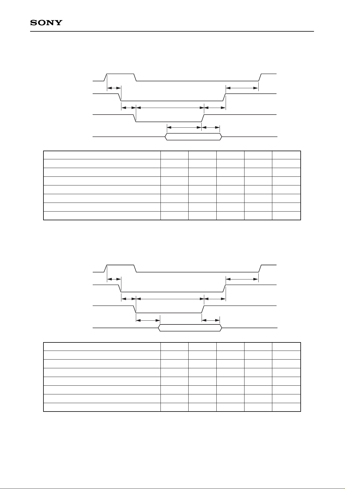
CXD1198AQ
6. Drive interface
(1) Read
(2) Write
A0 to 1
XCS
XRD
DA0 to 1
XDCS, XDRD
DDB0 to 7
DB0 to 7
t
DAD
tSCR
tDRR1
tDDD
tFRD
tDRR2
XCS
XWR
DB0 to 1
XDCS, XDWR
DDB0 to 7
t
SCW
tDWW1
tDDD2 tFWD
tDWW2
tHWD
Item
Drive address delay time (vs. A1 to 0)
Chip select setup time (vs. XRD↓)
Drive read signal delay time (vs. XRD↓)
CPU data delay time (vs. DDB0 to 7)
Drive read signal delay time (vs. XRD↑)
Data float time (vs. XDRD↑)
Chip select setup time (vs. XWR↓)
Drive write signal delay time (vs. XWR↓)
Data delay time (vs. DB0 to 7)
Data hold time (vs. XWR↑)
Drive write signal delay time (vs. XWR↑)
Data float time (vs. XWR↑)
Symbol
tDAD
tSCR
tDRR1
tDDD
tDDR2
tFRD
tSCW
tDWW1
tDDD2
tHWD
tDWW2
tFWD
Min.
0
0
0
10
TW
Typ.
27
24
Max.
45
35
70
30
70
Unit
ns
ns
ns
ns
ns
ns
ns
ns
ns
ns
ns
ns
TW is 1/f here.
—13—
CXD1198AQ
7. Drive DMA cycle
(1) Read
(2) Write
DDRQ
XDAC
XDRD
DDB0 to 7
t
DDA
tDAR
tSRD tHRD
tDARS
tRRL
tDRA
Item
XDAC fall time (vs. DDRQ↑)
DDRQ cycle time (vs. XDAC↑)
XDRD delay time (vs. XDAC↓)
XDAC delay time (vs. XDRD↑)
Low-level XDRD pulse width
Data setup time (vs. XDRD↓)
Data hold time (vs. XDRD↓)
Symbol
tDDA
tDARS
tDAR
tDRA
tRRL
tSRD
tHRD
Min.
0
25
0
Typ.
2TW+10
Max.
TW+32
TW
8
TW–5
Unit
ns
ns
ns
ns
ns
ns
ns
DDRQ
XDAC
XDWR
DDB0 to 7
t
DDA
tDAW
tDDW tFWD
tDAR
tWWL
tDWA
Item
XDAC fall time (vs. DDRQ↑)
DDRQ rise time (vs. XDAC↑)
XDWR delay time (vs. XDAC↓)
XDAC delay time (vs. XDWR↑)
Low-level XDWR pulse width
Data delay time (vs. XDWR↓)
Data float time (vs. XDWR↑)
Symbol
tDDA
tDARS
tDAW
tDWA
tWWL
tDDW
tFWD
Min.
2TW+5
10
Typ. Max.
TW+32
TW
5
TW
2TW+18
60
Unit
ns
ns
ns
ns
ns
ns
ns
TW is 1/f here.
TW is 1/f here.

—14—
CXD1198AQ
Description of Functions
1. Pin description
1-1. Drive interface (16 pins)
(1) DDB0 to 7 (Drive Data Bus : bidirectional)
Data bus input/output signals connected with the CXD1186BQ; connected to the HDB0 to 7 pins of the
CXD1186BQ.
(2) DDBP (Drive Data Pointer : bidirectional)
Error pointer input/output signal connected with the CXD1186BQ; connected to the HDBE pin of the
CXD1186BQ.
(3) XDCS (Drive Chip Select : negative logic output)
Chip select negative logic output signal for reading/writing host interface registers of the CXD1186BQ;
connected to the XHCS pin of the CXD1186BQ. The host interface registers of the CXD1186BQ are
mapped in 20H to 23H within register address space (00H to 3FH) of this IC.
(4) XDWR (Drive Write Strobe : negative logic output)
Strobe negative logic output signal for writing data into host interface registers of the CXD1186BQ;
connected to the XHWR pin of the CXD1186BQ.
(5) XDRD (Drive Read Strobe : negative logic output)
Strobe negative logic output signal for reading data into host interface registers of the CXD1186BQ;
connected to the XHRD pin of the CXD1186BQ.
(6) DA0, 1 (Drive Address : output)
Address output signals to the CXD1186BQ; connected to the HA0 and 1 pins of the CXD1186BQ.
(7) DDRQ (Drive DMA Request : positive logic input)
DMA request input signal from the CXD1186BQ; connected to the HDRQ pin of the CXD1186BQ.
(8) XDAC (Drive Acknowledge : negative logic output)
DMA acknowledge negative logic output signal to the CXD1186BQ in response to DDRQ; connected to
the XHAC pin of the CXD1186BQ.
1-2. Host interface (18pins)
(1) HDB0 to 7 (Host Data Bus : bidirectional)
Data bus input/output signals connected with host or SCSI control LSI (CXD1185); connected to the D0 to
7 pins for the SCSI control LSI (CXD1185).
(2) HMDS (Host Mode Select : input)
Input signal for selecting host mode. When connected with Intel 80-series CPU bus, set to low or open;
when connected with the SCSI control LSI (CXD1185), set to high.

—15—
CXD1198AQ
(3) HDRQ/XSAC (Host DMA Request/SCSI DMA Acknowledge : output)
HMDS = low : DMA request positive logic signal to host
HMDS = high : DMA acknowledge negative logic signal to SCSI control LSI (CXD1185)
(4) XHAC/SDRQ (Host DMA Acknowledge/SCSI DMA Request : input)
HMDS = low : DMA acknowledge negative logic signal from host
HMDS = high : DMA request positive logic signal from SCSI control LSI (CXD1185)
(5) XHWR (Host Write Strobe : negative logic input/output)
HMDS = low : Data write strobe negative logic input signal from host
HMDS = high : Data write strobe negative logic output signal to SCSI control LSI (CXD1185);
connected to the /WED pin of SCSI control LSI (CXD1185)
(6) XHRD (Host Read Strobe : negative logic input/output)
HMDS = low : Data read strobe negative logic input signal from host
HMDS = high : Data read strobe negative logic output signal to SCSI control LSI (CXD1185);
connected to the /RED pin of SCSI control LSI (CXD1185)
(7) XHCS (Host Chip Select : negative logic input)
Pulled up by standard 50 kΩ resistance in the IC.
HMDS = low : Chip select negative logic input signal of host
HMDS = high : Not used; set to high or open
(8) HA0, 1 (Host Address : inputs)
Pulled up by standard 50 kΩ resistance in the IC.
HMDS = low : Address input signal from host
HMDS = high : Not used; set to high or open
(9) HINT (Host Interrupt : output)
Open drain output.
HMDS = low: Interrupt request signal to host
HMDS = high : Not used
(10) HINP (Host Interrupt Polarity : input)
Selects the polarity of the HINT signal; set to low when the HINT signal turns to Low active and high when
it turns to High active.
1-3. Buffer Memory Interface (21 pins)
(1) BDB0 to 7 (Buffer Data Bus : input/output)
Buffer memory data bus signals
(2) BA0 to 9 (Buffer Address : output)
Buffer memory address signals; the addresses are output to different pins depending on the setting value
of Bits 2 and 3 (Buffer Memory Size) of the Configuration Register: to BA0 to 7 at 64 kB, to BA0 to 8 at
256 kB and to BA0 to 9 at 1 MB.

—16—
CXD1198AQ
(3) XRAS (Row Address Strobe : negative logic output)
Strobe negative logic output signal for row address in dynamic RAM.
(4) XCAS (Column Address Strobe : negative logic output)
Strobe negative logic output signal for column address in dynamic RAM.
(5) XWE (Write Enable : negative logic output)
Strobe negative logic output signal for writing in dynamic RAM.
(Note) Use a DRAM with an access time of 80 ns or less in this IC.
1-4. Subcode Interface (4 pins)
(1) WFCK (Write Frame Clock : input)
Write frame clock input signal from the CXD2500; connected to the WFCK pin of the CXD2500.
(2) SBSY (Subcode Sync : positive logic input)
Subcode frame sync input signal from the CXD2500; connected to the SCOR pin of the CXD2500.
(3) SBSI (Subcode Serial Input : input)
Channel P-W subcode data input signal from the CXD2500; connected to the SBSO pin of the CXD2500.
(4) EXCK (External Clock : output)
Readout clock signal to the CXD2500 for reading channel P-W subcode data input to SBSI; connected to
the EXCK pin of the CXD2500.
1-5. CPU Interface (19 pins)
(1) DB0 to 7 (CPU Data Bus : input/output)
8-bit CPU data bus signals
(2) A0 to 5 (CPU Address : input)
Address input signals for selecting this IC internal register and the host interface registers of the
CXD1186BQ from the CPU
(3) XWR (CPU Write : negative logic input)
Strobe negative logic input signal for the CPU to write data into this IC internal register and the host
interface registers of the CXD1186BQ.
(4) XRD (CPU Read : negative logic input)
Strobe negative logic input signal for the CPU to read data from this IC internal register and the host
interface registers of the CXD1186BQ.
 Loading...