

Sony CXD1186CR, CXD1186CQ Datasheet

—1—
E93512A78-TE
Sony reserves the right to change products and specifications without prior notice. This information does not convey any license by
any implication or otherwise under any patents or other right. Application circuits shown, if any, are typical examples illustrating the
operation of the devices. Sony cannot assume responsibility for any problems arising out of the use of these circuits.
Absolute Maximum Ratings (Ta=25 °C)
• Supply voltage VDD –0.5 to +7.0 V
• Input voltage VI –0.5 to VDD +0.5 V
• Output voltage VO –0.5 to VDD +0.5 V
• Operating temperature Topr –20 to +75 °C
• Storage temperature Tstg –55 to +150 °C
Recommended Operating Conditions
• Supply voltage VDD +4.5 to +5.5 V
(standard +5.0)
• Operating temperature Topr –20 to +75 °C
Description
The CXD1186C is a CD-ROM decoder LSI.
Features
• Corresponds to CD-ROM, CD-I and CD-ROM XA
formats.
• Real time error correction. (Erasure correction
using C2 pointer from CD player.)
• Double speed playback.
• Connection to standard SRAM up to 64 K bytes, as
buffer memory, possible.
Applications
CD-ROM driver
Structure
Silicon gate CMOS IC
CD-ROM Decoder
CXD1186CQ CXD1186CR
80 pin QFP (Plastic) 80 pin LQFP (Plastic)
CXD1186CQ/CR
For the availability of this product, please contact the sales office.
—2—
CXD1186CQ/CR
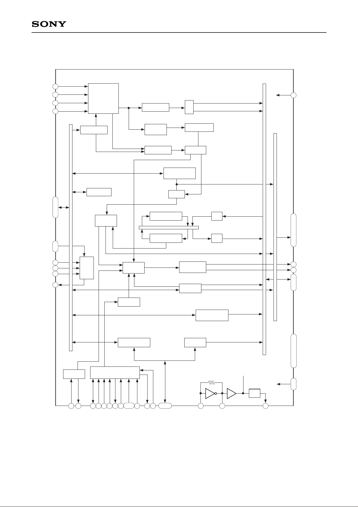
Block Diagram
DATA
BCLK
C2PO
LRCK
CDP I/F
CONTROL REG
DESCRAMBLE
SYNC
CONTROL
+2
HCLK
XTL2
XTL1
HDB0-7, P
HMDS
ADRQ
XAAC
HA0, 1
XTC
HINT
S/P
WORD CENTER
DECODETIMING GEN
DRIIVE ADDRESS
COUNTER
LATCH
REGISTERS
ECC
CONTROL
GALOIS FIELD
REG
REGSYNDROME
CPU
I/F
PRIORITY
RESOLVER
DMA
SEQUENCER
CPU DMA
DB0–7
A0–3
INT
HOST DMA
HOST ADDRESS
COUNTER
HOST I/F REGS DMA FIFO
ADP I/F
HOST I/F REGS
VDD
GND
BDB0–7, P
BA0–15
XRST
XWR
XRD
XCS
HDBP
XHWR
XHRD
XHCS
XDRQ
XHAC
XMWR
XMOE
—3—
CXD1186CQ/CR
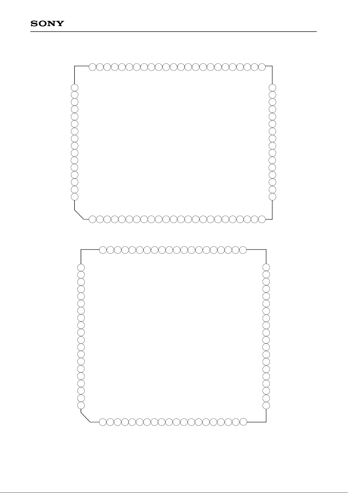
Pin Configuration
CXD1186CQ
1 2 3 4 5 6 7 8 9 10 11 14 1512 13 16 17 20 2118 19 23 24
25
26
27
28
29
30
31
32
33
34
35
36
37
38
39
40
22
64 63 62 61 60 59 58 57 56 55 54 51 5053 52 49 48 45 4447 46 42 4143
INT
GNDA0A1A2A3
HMDS
HA0
HA1
XHCS
HINT
GND
XHRD
XHWR
HDB0
HDB1
HDB2
HDB3
HDB4
HDB5
HDB6
HDB7
GND
HDBP
BA8
BA7
BA6
BA5
BA4
BA3
BA2
VDD
BA1
BA0
XAAC
ADRQ
XTC
XHAC
HDRQ
79
80
78
77
76
75
74
73
72
71
70
69
68
67
66
65
XRST
HCLK
GND
XTL1
XTL2
BDBP
BDB7
BDB6
BDB5
BDB4
BDB3
BDB2
BDB1
GND
BDB0
XMWR
XMOE
BA15
BA14
BA13
BA12
BA11
BA10
GND
BA9
LRCK
DATA
BCLK
C2PO
DB0
DB1
DB2
DB3
VDD
DB4
DB5
DB6
DB7
XCS
XRD
XWR
CXD1186CR
1 2 3 4 5 6 7 8 9 10 11 14 1512 13 16 172018 19
25
26
27
28
21
22
23
24
29
30
31
32
33
34
35
36
37
38
39
40
60 59 58 57 56 55 54 51 5053 52 49 48 45 4447 46 42 4143
A0A1A2A3HMDS
HA0
HA1
XHCS
HINT
GND
XHRD
XHWR
HDB0
HDB1
HDB2
HDB3
HDB4
HDB5
HDB6
HDB7
GND
BA9
BA8
BA7
BA6
BA5
BA4
BA3
BA1
V
DD
BA1
FA0
XAAC
ADRQ
XTC
79
80
78
77
76
75
74
73
72
71
70
69
68
67
66
65
XHAC
HDRQ
XRST
HDRP
GND
XTL1
XTL2
BDBP
BDB7
BDB6
BDB5
BDB4
BDB3
BDB2
BDB1
GND
BDB0
XMWR
XMOE
BA15
BA14
BA13
BA12
BA11
BA10
BCLK
C2PO
DB0
DB1
64
63
62
61
GND
HCLK
LRCK
DATA
DB2
DB3
V
DD
DB4
DB5
DB6
DB7
XCS
XRD
XWR
INT
GND
—4—
CXD1186CQ/CR
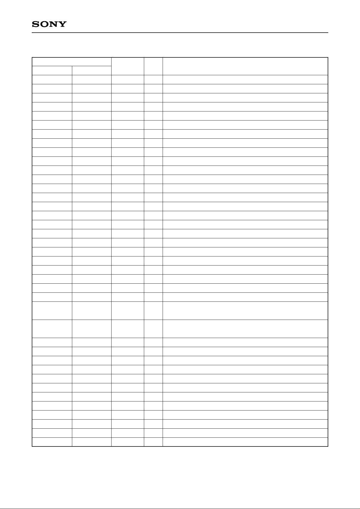
Pin Description
Pin No.
Symbol I/O Description
CXD1186CQ CXD1186CR
1
2
3
4
5
6
7
8
9
10
11
12
13
14
15
16
17
18
19
20
21
22
23
24
25
26
27
28
29
30
31
32
33
34
35
36
37
38
39
79
80
1
2
3
4
5
6
7
8
9
10
11
12
13
14
15
16
17
18
19
20
21
22
23
24
25
26
27
28
29
30
31
32
33
34
35
36
37
INT
GND
A0
A1
A2
A3
HMDS
HA0
HA1
XHCS
HINT
GND
XHRD
XHWR
HDB0
HDB1
HDB2
HDB3
HDB4
HDB5
HDB6
HDB7
GND
HDBP
XRST
HDRQ
XHAC
XTC
ADRQ
XAAC
BA0
BA1
VDD
BA2
BA3
BA4
BA5
BA8
BA7
O
—
I
I
I
I
I
I
I
I
O
—
I/O
I/O
I/O
I/O
I/O
I/O
I/O
I/O
I/O
I/O
—
I/O
I
O
I
I
I
O
O
O
—
O
O
O
O
O
O
Interrupt request signal to CPU
GND pin
CPU address signal
CPU address signal
CPU address signal
CPU address signal
Host mode select signal
Host address signal
Host address signal
Chip select negative logic signal from host
Interrupt request negative logic signal to host
GND pin
Data read strobe signal from host or to SCSI control IC
Data write strobe signal from host or to SCSI control IC
Host data bus
Host data bus
Host data bus
Host data bus
Host data bus
Host data bus
Host data bus
Host data bus
GND pin
Error flag, Host data bus
Reset negative logic signal
Data request positive logic signal to host. Or DMA
acknowledge negative logic signal to SCSI control IC
DMA acknowledge negative logic signal from host.
Or data request positive logic signal from SCSI control IC
Terminal count negative logic signal
DMA request positive logic signal from ADP
DMA acknowledge negative logic signal to ADP
Buffer memory address
Buffer memory address
Power (+5 V) supply pin
Buffer memory address
Buffer memory address
Buffer memory address
Buffer memory address
Buffer memory address
Buffer memory address

—5—
CXD1186CQ/CR
Pin No.
Symbol I/O Description
CXD1186CQ CXD1186CR
40
41
42
43
44
45
46
47
48
49
50
51
52
53
54
55
56
57
58
59
60
61
62
63
64
65
66
67
68
69
70
71
72
73
74
75
76
77
78
79
80
38
39
40
41
42
43
44
45
46
47
48
49
50
51
52
53
54
55
56
57
58
59
60
61
62
63
64
65
66
67
68
69
70
71
72
73
74
75
76
77
78
BA8
BA9
GND
BA10
BA11
BA12
BA13
BA14
BA15
XMOE
XMWR
BDB0
GND
BDB1
BDB2
BDB3
BDB4
BDB5
BDB6
BDB7
BDBP
XTL2
XTL1
GND
HCLK
LRCK
DATA
BCLK
C2PO
DB0
DB1
DB2
DB3
VDD
DB4
DB5
DB6
DB7
XCS
XRD
XWR
O
O
—
O
O
O
O
O
O
O
O
I/O
—
I/O
I/O
I/O
I/O
I/O
I/O
I/O
I/O
O
I
—
O
I
I
I
I
I/O
I/O
I/O
I/O
—
I/O
I/O
I/O
I/O
I
I
I
Buffer memory address
Buffer memory address
GND pin
Buffer memory address
Buffer memory address
Buffer memory address
Buffer memory address
Buffer memory address
Buffer memory address
Buffer memory output enable negative logic signal
Buffer memory write negative logic signal
Buffer memory data bus
GND pin
Buffer memory data bus
Buffer memory data bus
Buffer memory data bus
Buffer memory data bus
Buffer memory data bus
Buffer memory data bus
Buffer memory data bus
Buffer memory pointer data bus
Crystal oscillation circuit output pin
Crystal oscillation circuit input pin
GND pin
1/2 frequency divided clock signal of XTL1
LR clock from CD player
Serial data from CD player
Bit clock from CD player
C2 pointer from CD player
CPU data bus
CPU data bus
CPU data bus
CPU data bus
Power (+5 V) supply pin
CPU data bus
CPU data bus
CPU data bus
CPU data bus
Chip select negative logic signal from CPU
CPU strobe negative logic signal to read out this IC internal
register
CPU strobe negative logic signal to write in this IC internal
register

—6—
CXD1186CQ/CR
Electrical Characteristics
DC characteristics (VDD=5 V±10 %, VSS=0 V, Topr=–20 to +75 °C)
Item
Input voltage
H level
L level
TTL Schmitt hysterisis
Input current of pull up input
Input current of pull down input
Output voltage
H level
L level
Open drain output L level
Oscillation cell H level
input voltage L level
Logic threshold value
Feedback resistance
Output voltage
H level
L level
Symbol
VIH1
VIL1
(Vt+)–(Vt–)
IIL
IIH
VOH1
VOL1
VOL2
VIH
VIL
LVth
RFB
VOH
VOL
Conditions
VIL=0 V
VIH=VDD
IOH=–2 mA
IOL=4 mA
IOL=4 mA
VIN=VSS or VDD
IOH=–1 mA
IOL=1 mA
Min. Typ. Max. Unit
2.2 V
0.8 V
0.2 0.4 V
–40 –100 –240 µA
40 100 240 µA
VDD–0.8 V
0.4 V
0.4 V
0.7 VDD V
0.3 VDD V
VDD/2 V
250 k 1 M 2.5 M Ω
VDD/2 V
VDD/2 V
• Input pin with pull up resistance : XHCS, HA0, HA1, XTC
• Input pin with pull down resistance : C2PO, HMDS, ADRQ
• TTL Schmitt input pin : XRST
• Open drain output pin : HINT
• Two-way data bus always pulled up.
• Oscillation cell
Input : XTL1
Output : XTL2
I/O capacitance VDD=VI=0 V, f=1 MHz
Item
Input pin
Output pin
I/O pin
Symbol
CIN
COUT
CI/O
Min. Typ. Max.
9
11
11
Unit
pF
pF
pF
—7—
CXD1186CQ/CR
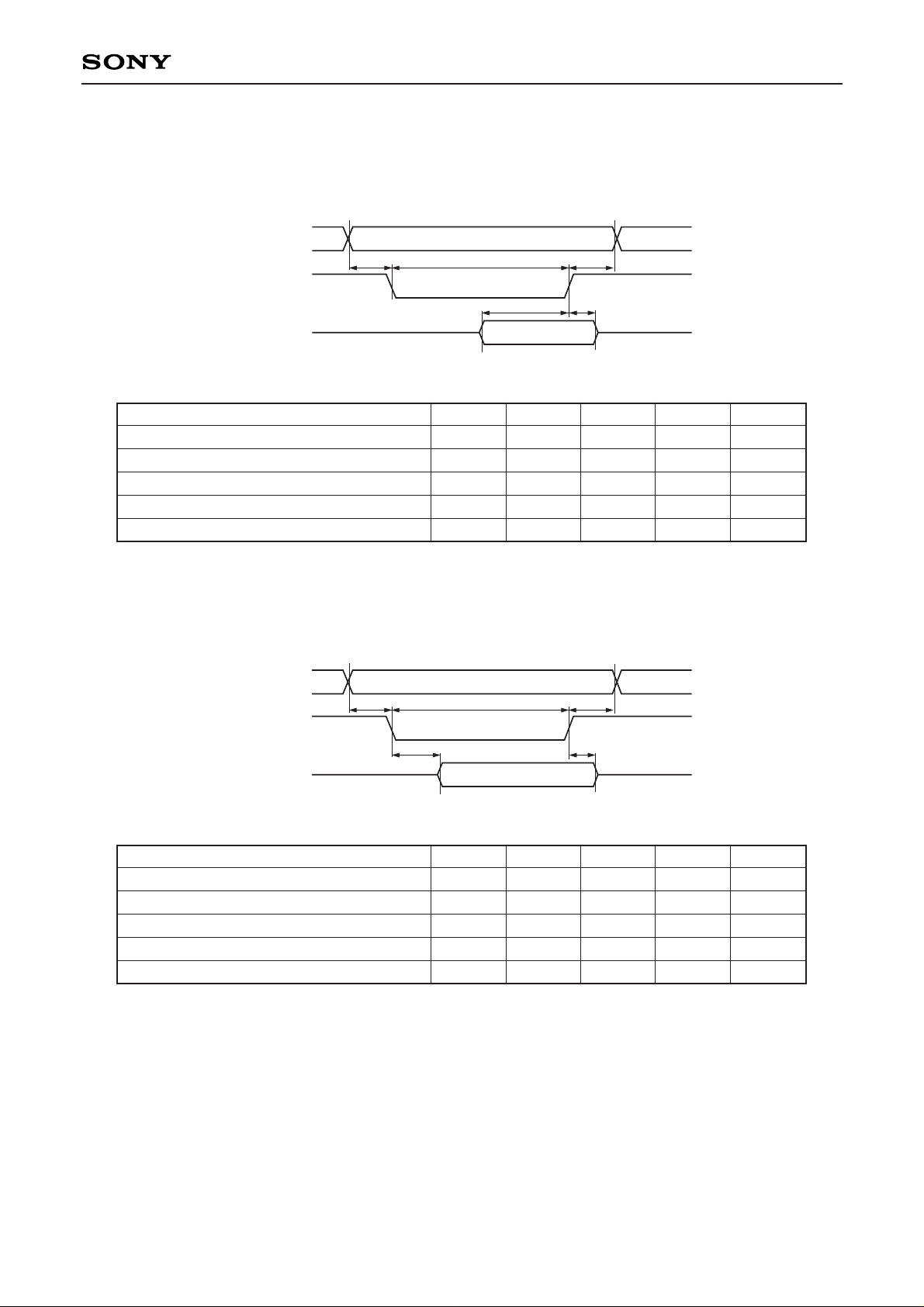
AC characteristics (Ta=–20 to +75 °C, VDD=5 V±10 %, Output Load=50 pF, f≤ 24.576 MHz)
1. CPU interface
(1) Read
(2) Write
A0 to 3
XCS
XRD
DB0 to 7
t
HRA
tRRL
tSAR tDRD
tFRD
Item
Address setup time (vs. XCS & XRD ↓)
Address hold time (vs. XCS & XRD ↑)
Data delay time (vs. XCS & XRD ↓)
Data float time (vs. XCS & XRD ↑)
Low level XRD pulse width
Symbol
tSAR
tHRA
tDRD
tFRD
tRRL
Min.
30
20
0
100
Typ. Max.
60
10
Unit
n
n
n
n
n
A0 to 3
XCS
XWR
DB0 to 7
t
HWD
tHWA
tSDW
tWWL
tSAW
Item
Address setup time (vs. XCS & XWR ↓)
Address hold time (vs. XCS & XWR ↑)
Data setup time (vs. XCS & XWR ↑)
Data hold time (vs. XCS & XWR ↑)
Low level XWR pulse width
Symbol
tSAW
tHWA
tSDW
tHWD
tWWL
Min.
30
20
40
10
50
Typ. Max. Unit
n
n
n
n
n
Where & in the chart indicates logical multiplication.
—8—
CXD1186CQ/CR
2. Memory interface
(1) Read
(2) Write
BA0 to 15
tRRLtSAO tHOA
tHOD
tSDO
XMOE
BDB0 to 7, P
Item
Address setup time (vs. XMOE ↓)
Address hold time (vs. XMOE ↑)
Data setup time (vs. XMOE ↑)
Data hold time (vs. XMOE ↑)
Low level XMOE pulse width
Symbol
tSAO
tHOA
tSDO
tHOD
tRRL
Min.
Tw–22
Tw–9
45
0
2 • Tw
Typ. Max.
2•Tw+16
Unit
n
n
n
n
n
BA0 to 15
t
WWL
tSAW tHWA
tFWD
tDWD
XMWR
BDB0 to 7, P
Item
Address setup time (vs. XMWR ↓)
Address hold time (vs. XMWR ↑)
Data delay time (vs. XMWR ↓)
Data float time (vs. XMWR ↑)
Low level XMWR pulse width
Symbol
tSAW
tHWA
tDWD
tFWD
tWWL
Min.
Tw–29
Tw–9
10
2 • Tw
Typ. Max.
0
Unit
n
n
n
n
n
Where Tw=1/f.
Usually, when f=16.9344 MHz, use a RAM with access time within 120 ns.
—9—
CXD1186CQ/CR
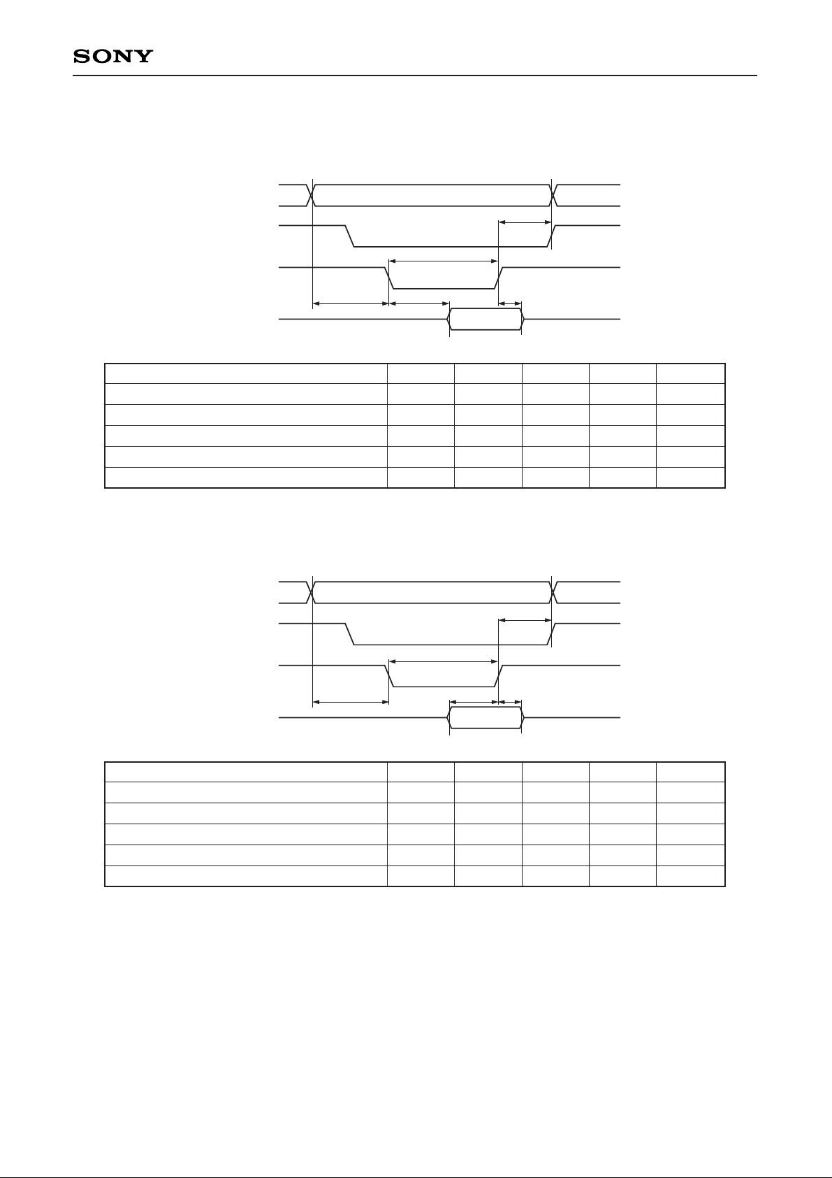
3. Host interface
(1) Read
(2) Write
HA0 to 1
tHRA
tRRL
tFRD
tDRDtSAR
XHCS
XHRD
HDB0 to 7, P
Item
Address setup time (vs. XHCS & XHRD ↓)
Address hold time (vs. XHCS & XHRD ↑)
Data delay time (vs. XHCS & XHRD ↓)
Data float time (vs. XHCS & XHRD ↑)
Low level XHRD pulse width
Symbol
tSAR
tHRA
tDRD
tFRD
tRRL
Min.
30
20
0
100
Typ. Max.
60
10
Unit
n
n
n
n
n
HA0 to 1
tSAW
tWWL
tSDW
tHWD
tHWA
XHCS
XHWR
HDB0 to 7, P
Item
Address setup time (vs. XHCS & XHWR ↓)
Address hold time (vs. XHCS & XHWR ↑)
Data setup time (vs. XHCS & XHWR ↑)
Data hold time (vs. XHCS & XHWR ↑)
Low level XHWR pulse width
Symbol
tSAW
tHWA
tSDW
tHWD
tWWL
Min.
30
20
40
10
50
Typ. Max. Unit
n
n
n
n
n

—10—
CXD1186CQ/CR
4. HOST DMA cycle (80 type bus)
(1) Read
(2) Write
HDRQ
t
DAR2
tHRA
tRRL
tSAR
tDAR1
tDRD
tFRD
XHAC
XHRD
HDB0 to 7, P
Item
HDRQ fall time (vs. XHAC ↓)
HDRQ rise time (vs. XHAC ↑)
XHAC setup time (vs. XHRD ↓)
XHAC hold time (vs. XHRD ↑)
Low level XHRD pulse width
Data delay time (vs. XHRD ↓)
Data float time (vs. XHRD ↑)
Symbol
tDAR1
tDAR2
tSAR
tHRA
tRRL
tDRD
tFRD
Min.
5
0
100
0
Typ. Max.
35
48
60
10
Unit
n
n
n
n
n
n
n
HDRQ
t
SAW
tWWL
tHWA
tHWD
tSDW
tDAR1
tDAR2
XHAC
XHWR
HDB0 to 7, P
Item
HDRQ fall time (vs. XHAC ↓)
HDRQ rise time (vs. XHAC ↑)
XHAC setup time (vs. XHWR ↓)
XHAC hold time (vs. XHWR ↑)
Low level XHWR pulse width
Data setup time (vs. XHWR ↑)
Data hold time (vs. XHWR ↑)
Symbol
tDAR1
tDAR2
tSAW
tHWA
tWWL
tSDW
tHWD
Min.
5
0
50
40
10
Typ. Max.
35
48
Unit
n
n
n
n
n
n
n

—11—
CXD1186CQ/CR
5. HOST DMA cycle (SCSI bus)
(1) Read
(2) Write
SDRQ
tDDA
tDAR
tRRL
tDRA
tHRD
tDRD
XSAC
XHRD
HDB0 to 7, P
Item
XSAC fall time (vs. SDRQ ↑)
XSAC delay time (vs. XHRD ↓)
XSAC delay time (vs. XHRD ↑)
Low level XHRD pulse width
Data delay time (vs. XHRD ↓)
Data hold time (vs. XHRD ↑)
Symbol
tDDA
tDAR
tDRA
tRRL
tDRD
tHRD
Min.
0
T+59
0
Typ. Max.
Tw
Tw
90
Unit
n
n
n
n
n
n
SDRQ
tDDA
tDAW tWWL tDWA
tFWD
tSDW
XSAC
XHWR
HDB0 to 7, P
Item
XSAC fall time (vs. SDRQ ↑)
XHWR delay time (vs. XSAC ↓)
XSAC delay time (vs. XHWR ↑)
Low level XHWR pulse width
Data setup time (vs. XHWR ↓)
Data float time (vs. XHWR ↓)
Symbol
tDDA
tDAW
tDWA
tWWL
tSDW
tFWD
Min.
T
T+24
27
Typ. Max.
Tw
Tw
Tw
Unit
n
n
n
n
n
n
Where T in the chart indicates :
Tw for 3 cycle mode
2 • Tw for 4 cycle mode
3 • Tw for 5 cycle mode
Here Tw=1/f

—12—
CXD1186CQ/CR
6. ADPCM DMA cycle
Where T in the chart indicates :
Tw for 3 cycle mode
2 • Tw for 4 cycle mode
3 • Tw for 5 cycle mode
Here Tw=1/f
7. XTL1 and XTL2 pins
(1) For self oscillation (Topr=–20 to +75 °C, VDD=5.0 V±10 %)
(2) When a pulse is input to XTL1 (Topr=–20 to +75 °C, VDD=5.0 V±10 %)
ADRQ
tWWL tDWAtDAW
tDDA
tSDW
tFWD
XAAC
XHWR
HDB0 to 7, P
Item
XAAC fall time (vs. ADRQ ↑)
XHWR delay time (vs. XAAC ↓)
XAAC delay time (vs. XHWR ↑)
Low level XHWR pulse width
Data setup time (vs. XHWR ↓)
Data float time (vs. XHWR ↓)
Symbol
tDDA
tDAW
tDWA
tWWL
tSDW
tFWD
Min.
T
T+24
27
Typ. Max.
Tw
Tw
Tw
Unit
n
n
n
n
n
n
tW
tR tF
tWHX tWLX
tILX
VIHX
VIHX X0.9
VIHX X0.1
VDD/2
XTL1
Item
“H” level pulse width
“L” level pulse width
Pulse period
Input “H” level
Input “L” level
Rise time, Fall time
Symbol
tWHX
tWLX
tW
VIHX
VILX
tR, tF
Min.
15
15
40.7
VDD—1.0
Typ. Max.
0.8
15
Unit
ns
ns
ns
V
V
ns
Item
Oscillation frequency
Symbol
fMAX
Min.
16.9344
Typ. Max.
24.576
Unit
MHz

—13—
CXD1186CQ/CR
Description of Function
1. Pin description
Below is a description of pins by function.
1.1 CD player interface (4 pins)
(1) DATA (input)
Serial data from CIRC LSI (digital signal processing LSI for CD)
(2) BCLK (input)
Bit clock. Clock for DATA Strobe.
(3) LRCK (input)
LR clock. Indicates LCH and RCH of DATA input.
(4) C2PO (positive logic input)
C2 pointer signal from CIRC. Indicates an error is included in the DATA input.
Interface mode with the CD player is controlled at DRVIF register.
1.2 Buffer memory interface (27 pins)
(1) XMWR (memory write, negative logic output)
Data write strobe signal of the buffer memory.
(2) XMOE (memory output enable, negative logic output)
Data read strobe signal of the buffer memory.
(3) BA0 to 15 (Buffer memory address, output)
Address signal of the buffer memory.
(4) BDB0 to 7 (Buffer data bus, I/O)
Data bus signal of the buffer memory.
(5) BDBP (Buffer data bus, I/O)
Buffer memory data bus signal for error pointer.
1.3 CPU interface (16 pins)
(1) XWR (CPU write, negative logic input)
Write strobe signal of the CPU register.
(2) XRD (CPU read, negative logic input)
Read out strobe signal of the CPU register.
(3) XCS (CPU chip select, negative logic input)
Chip select negative logic signal from the CPU.
(4) A0 to 3 (CPU address, input)
Address signal for the CPU selection of the IC internal register.
(5) DB0 to 7 (CPU data bus, I/O)
CPU data bus signal.
(6) INT (CPU interrupt, output)
Interrupt request output to the CPU. This pin polarity is controlled at the CONFIG register.
1.4 Host interface (19 pins)
(1) HMDS (Host mode select, input)
Signal for the host mode selection. This pin is pulled down inside the IC by means of a resistor at a
standard 50 kΩ.
“L” or open : connected to Intel 80 type host Bus.
“H” : connected to SCSI controller IC.
(2) HDRQ/XSAC (Host data request/SCSI acknowledge, output)
When HMDS is at “L”, DMA data request positive logic signal to host.
When HMDS is at “H”, DMA acknowledge negative logic signal to SCSI control IC.

—14—
CXD1186CQ/CR
(3) XHAC/SDRQ (Host DMA acknowledge/SCSI data request, input)
When HMDS is at “L”, DMA acknowledge negative logic signal from host.
When HMDS is at “H”, DMA data request positive logic signal from SCSI control IC.
(4) XHWR (Host write, negative logic I/O)
When HMDS is at “L” and ADMAEN (DMACTL register, bit4) also at “L”, data write strobe input from
host.
When HMDS is at “H” and ADMAEN at “L”, data write strobe output to SCSI control IC.
When ADMAEN is at “H”, data write strobe output to audio processor (ADP).
(5) XHRD (Host read, negative logic I/O)
When HMDS is at “L” and ADMAEN also at “L”, data read strobe input from host.
When HMDS is at “H” and ADMAEN at “L”, data read strobe output to SCSI control IC.
When ADMAEN is at “H”, data read strobe output to ADP.
(6) XHCS (Host chip select, negative logic input)
This pin is pulled up inside the IC by means of a resistor at a standard 50 kΩ.
When HMDS is at “L”, chip select input from host.
When HMDS is at “H”, this signal is not used. Either fix to “H” or keep open.
(7) HA0 and 1 (Host address, input)
These pins are pulled up inside the IC by means of a resistor at a standard 50 kΩ.
When HMDS is at “L”, address input from the host.
When HMDS is at “H”, these signals are not used. Either fix to “H” or keep open.
(8) HDB0 to 7 (Host data bus, I/O)
Host data bus signal.
(9) HDBP (Host data bus, I/O)
Host data bus signal for error pointer.
(10) HINT (HOST interrupt, output)
This pin is an open drain output.
When HMDS is at “L”, interrupt request negative logic output to host.
When HMDS is at “H”, this signal is not used.
(11) XTC (Terminal count, negative logic output)
This is pulled up inside the IC by means of a resistor at a standard 50 kΩ.
When HMDS is at “L”, data transfer complete instruction negative logic input from the host.
When HMDS is at “H”, this signal is not used. Either fix to “H” or keep open.
1.5 Audio processor (ADP) interface (2 pins)
(1) ADRQ (audio processor DMA request, positive logic input)
This pin is pulled down inside the IC by means of a resistor at a standard 50 kΩ.
DMA data request signal to ADP. When not connected to ADP and CXD1186Q, either fix to “L” or keep
open.
(2) XAAC (audio processor DMA acknowledge, negative logic output)
DMA acknowledge signal from ADP.
1.6 Others (4 pins)
(1) XTL1 (Crystal1, input)
(2) XTL2 (Crystal2, output)
Crystal oscillator connecting pin for master clock oscillation.
(3) HCLK (halfclock, output)
Half frequency divided clock of the master clock.
(4) XRST (Reset, negative logic input)
Chip reset signal.
Pins BDB0 to 7, BDBP, DB0 to 7, HDB0 to 7 and HDBP are pulled up inside the IC by means of a
resistor at a standard 25 kΩ.
 Loading...