

Sony CXD1185CR, CXD1185CQ Datasheet

—1—
E92905B78-TE
Sony reserves the right to change products and specifications without prior notice. This information does not convey any license by
any implication or otherwise under any patents or other right. Application circuits shown, if any, are typical examples illustrating the
operation of the devices. Sony cannot assume responsibility for any problems arising out of the use of these circuits.
• Supports SCSI phase commands.
• All SCSI control signal are software controllable.
• All interrupt conditions are software maskable.
• Built-in 4-bit general-use I/O port.
• Programmable SCSI RST drive time.
• Programmable interrupt pin (IRQ) active logic level.
• Single initiator mode detection logic.
• Selection phase SCSI parity check/ignore switch.
• Pin compatible with CXD1185AQ.
(CXD1185CQ only)
• Comes in 64-pin QFP or 64-pin LQFP
Applications
SCSI controller
Structure
CMOS Process
Absolute Maximum Ratings (Ta=25 °C, VSS=0 V)
• Supply voltage VDD VSS–0.5 to +7.0 V
• Input voltage VI VSS–0.5 to VDD +0.5 V
• Output voltage VO VSS–0.5 to VDD +0.5 V
• Operating temperature
Topr –20 to +75 °C
• Storage temperature
Tstg –55 to +150 °C
Description
The CXD1185C is a high performance CMOS
SCSI controller LSI that conforms to ANSIX3. 1311986 standards. The CXD1185C is capable of
operating in both initiator and target modes. It
satisfies all standard SCSI bus features, such as
arbitration, selection and parity generation/check
functions. A 24-bit data transfer byte counter and
16-byte FIFO are built into the hardware. Two
separate buses for data and processor makes high
speed data transfer possible. 48 mA (sinking) port
is built-in to achieve reduction in the number of
external components.
The chip offers a set of high level commands at
SCSI phase level. It is also possible to read/write all
individual SCSI signals. The combination of the
above two makes programs simpler and at the same
time improves programmability.
Features
• Satisfies all SCSI bus features, including
arbitration, selection, parity generation/check and
synchronous data transfer.
• Maximum synchronous data transfer rate of 4.0
MB/s and maximum asynchronous data transfer
rate of 2.5 MB/s.
• Provides two separate ports for the data bus and
the CPU bus.
• Built-in user-programmable timer for selection
/reselection time-out operation.
• Supports 8-bit microcomputer bus.
• Support programmed I/O and DMA transfer.
• Built-in 48 mA (sinking) SCSI port. The SCSI port
can be used as either single-ended port or
differential port.
• Built-in 24-bit data transfer counter.
• Built-in 16-byte FIFO.
SCSI 1 Protocol Controller
CXD1185CQ CXD1185CR
64 pin QFP (Plastic) 64 pin LQFP (Plastic)
CXD1185CQ/CR
For the availability of this product, please contact the sales office.

—2—
CXD1185CQ/CR
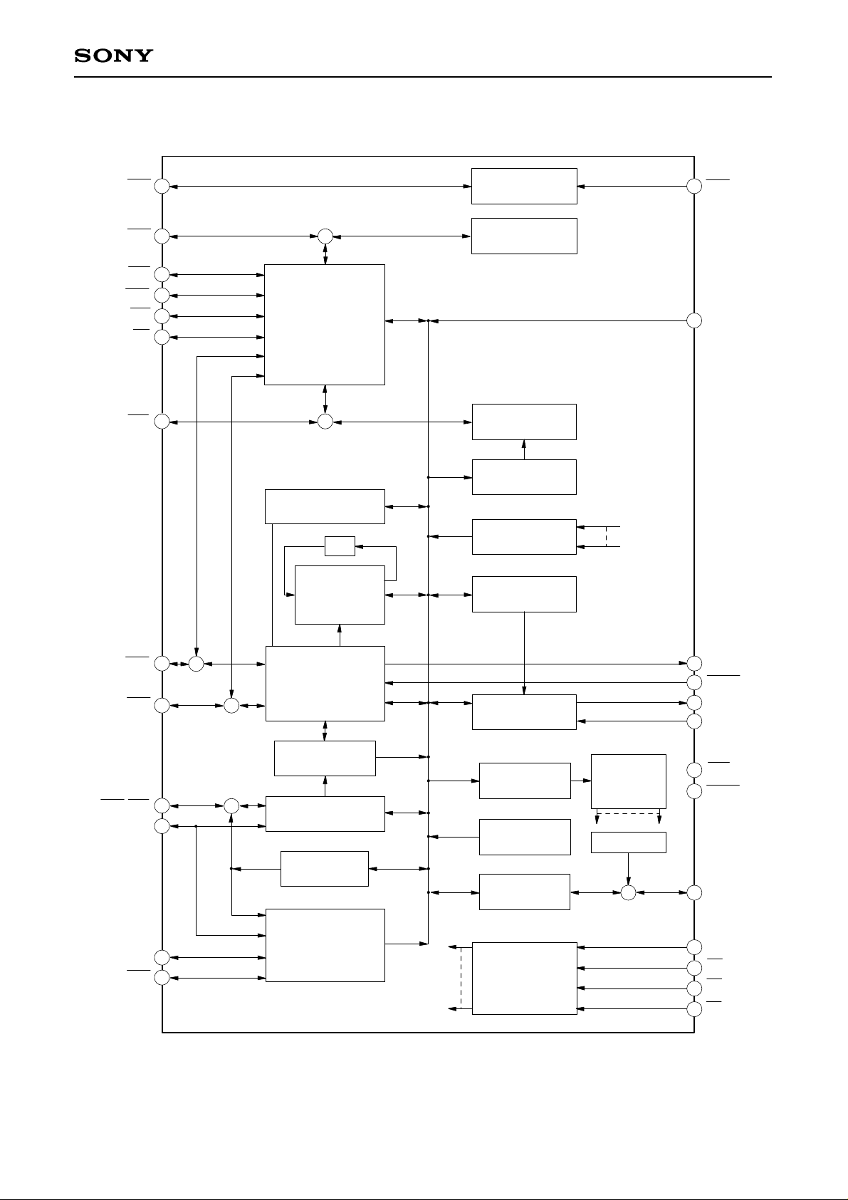
Block Diagram (CXD1185CQ)
20 29
18
17
22
24
28
23
25 43
44
42
57
59
60
19
55
15
+
+
+
+
+
+
30
32
31
RST RES
DRQ
IRQ
CLK
BSY
ATN
MSG
C/D
I/O
SEL
REQ
ACK
DBP
DB7-DB0
D7-D0
5, 7-10, 12-14
47-54
DP
Sync Transfer Control
–1
Transfer Byte
Counter
DMA Control
FIFO Counter
FIFO
ID
Time-Out
Interrupt Request
Interrupt Mask
Configuration
Command
Status
General-Use
I/O Port
Decode
33-40
C7-C0
61-64
P3-P0
1-4
A3-A0
DACK
INIT
TARG
CS
WE
RE
Command
Interpreter
Differential
Control
SCSI
Control
Parity
Generate/Check
Reset
Control
Arbiration
Control
Selection
Control
—3—
CXD1185CQ/CR
Block Diagram (CXD1185CR)
18 27
16
15
20
22
26
21
23 41
42
40
55
57
58
17
53
13
+
+
+
+
+
+
28
30
29
RST RES
DRQ
IRQ
CLK
BSY
ATN
MSG
C/D
I/O
SEL
REQ
ACK
DBP
DB7-DB0
D7-D0
3, 5-8, 10-12
45-52
DP
Sync Transfer Control
–1
DMA Control
FIFO Counter
FIFO
ID
Interrupt Request
Interrupt Mask
Configuration
Command
Status
31-38
C7-C0
59-62
P3-P0
63, 64, 1, 2
A3-A0
DACK
INIT
TARG
CS
WE
RE
Differential
Control
SCSI
Control
Reset
Control
Arbiration
Control
Selection
Control
Time-Out
Transfer Byte
Counter
Parity
Generate/Check
Decode
General-Use
I/O Port
Command
Interpreter

—4—
CXD1185CQ/CR
Pin Configuration
CXD1185CQ
51 33
52
64
1 19
20
32
CXD1185CR
48
49
33
32
64
1 16
17
Pin Description
Pin No.
Symbol I/O Description
CXD1185CQ CXD1185CR
1
2
3
4
5
6
7
8
9
10
11
12
13
14
15
16
17
18
19
20
21
22
23
24
25
26
27
28
63
64
1
2
3
4
5
6
7
8
9
10
11
12
13
14
15
16
17
18
19
20
21
22
23
24
25
26
A3
A2
A1
A0
DB0
VSS
DB1
DB2
DB3
DB4
VSS
DB5
DB6
DB7
DBP
VSS
ATN
BSY
ACK
RST
VSS
MSG
SEL
C/D
REQ
VDD
VSS
I/O
I
I
I
I
I/O
I/O
I/O
I/O
I/O
I/O
I/O
I/O
I/O
I/O
I/O
I/O
I/O
I/O
I/O
I/O
I/O
I/O
Register select signal bit 3
Register select signal bit 2
Register select signal bit 1
Register select signal bit 0
SCSI bus DB0 signal
GND <note 1>
SCSI bus DB1 signal
SCSI bus DB2 signal
SCSI bus DB3 signal
SCSI bus DB4 signal
GND <note 1>
SCSI bus DB5 signal
SCSI bus DB6 signal
SCSI bus DB7 signal
SCSI bus DBP signal, odd parity
GND <note 1>
SCSI bus ATN signal
SCSI bus BSY signal
SCSI bus ACK signal
SCSI bus RST signal
GND <note 1>
SCSI bus MSG signal
SCSI bus SEL signal
SCSI bus C/D signal
SCSI bus REQ signal
+5 V <note1>
GND <note 1>
SCSI bus I/O signal

—5—
CXD1185CQ/CR
Pin No.
Symbol I/O Description
CXD1185CQ CXD1185CR
29
30
31
32
33
34
35
36
37
38
39
40
41
42
43
44
45
46
47
48
49
50
51
52
53
54
55
56
57
58
59
60
61
62
63
64
27
28
29
30
31
32
33
34
35
36
37
38
39
40
41
42
43
44
45
46
47
48
49
50
51
52
53
54
55
56
57
58
59
60
61
62
RES
CS
RE
WE
C7
C6
C5
C4
C3
C2
C1
C0
VSS
IRQ
DRQ
DACK
WED
RED
D0
D1
D2
D3
D4
D5
D6
D7
DP
VSS
CLK
VDD
INIT
TARG
P0 (DOE)
P1 (ARB)
P2 (BSYO)
P3 (SELO)
I
I
I
I
I/O
I/O
I/O
I/O
I/O
I/O
I/O
I/O
O
O
I
I
I
I/O
I/O
I/O
I/O
I/O
I/O
I/O
I/O
I/O
I
O
O
I/O
I/O
I/O
I/O
Reset all registers, negative logic
Chip select signal, negative logic
Internal register read signal, negative logic
Internal register write signal, negative logic
CPU bus bit 7
CPU bus bit 6
CPU bus bit 5
CPU bus bit 4
CPU bus bit 3
CPU bus bit 2
CPU bus bit 1
CPU bus bit 0
GND <note1>
Interrupt request signal
DMA request signal
DMA acknowledge signal, negative logic
Data bus write signal, negative logic <note3>
Data bus read signal, negative logic <note3>
Data bus bit 0 <note3>
Data bus bit 1 <note3>
Data bus bit 2 <note3>
Data bus bit 3 <note3>
Data bus bit 4 <note3>
Data bus bit 5 <note3>
Data bus bit 6 <note3>
Data bus bit 7 <note3>
Data bus parity signal <note4>
GND <note1>
Clock input, 5 –16 MHz
+5 V <note1>
Initiator operation indicator signal
Target operation indicator signal
General-use port bit 0 (SCSI data output authorization)
<note2>
General-use port bit 1 (arbitration in progress) <note2>
General-use port bit 2 (SCSI BSY output) <note2>
General-use port bit 3 (SCSI SEL output) <note2>
<Note1> All VDD and VSS pins should be connected to the power supply and ground, respectively.
<Note2> Items in parentheses ( ) indicate the meaning of the signal when operating in the SCSI differential
mode.
<Note3> In systems where the CPU and data buses are not separate, connect the WED and RED pins to
WE and RE, respectively, and Pins D7-D0 to Pins C7-C0.
<Note4> If the data bus parity signal is not used, pull up the DP pin using a resistor.

—6—
CXD1185CQ/CR
Electrical Characteristics
DC characteristics
I/O Capacitance
AC characteristics (Ta=–20 to +75 °C, VDD=5 V±10 %)
The following capacitances are assumed : input, output pins : 65 pF, input/output pins : 125 pF
Clock input
Reset input
Item
Supply voltage
High level input voltage
Low level input voltage
SCSI bus pin input voltage hysteresis
High level output voltage
Low level output voltage
SCSI bus pin output voltage
Input leak current
Input leak current (bidirectional pin)
Symbol
VDD
VIHT
VILT
(VT+)–(VT–)
VOH
VOL
VOLS
ILI1
ILI2
Conditions
IOH=–2 mA
IOL=4 mA
IOL=48 mA
Min. Typ. Max. Unit
4.5 5.0 5.5 V
2.2 V
0.8 V
0.2 V
VDD–0.5 V
0.4 V
0.5 V
–10 10 µA
–40 40 µA
Item
Input pin
Output pin
Input/Output pin
Symbol
CIN
COUT
CI/O
Min. Typ. Max.
9
11
11
Unit
pF
pF
pF
Item
Clock cycle
Clock pulse high level width (cycle : 16 MHz)
Clock pulse low level width (cycle : 16 MHz)
Symbol
Tcyc
Tcknw
Tcklw
Min.
5
31
31
Typ. Max.
16
33
33
Unit
MHz
ns
ns
Item
Reset pulse width
Symbol
Tresw
Min.
100
Typ. Max. Unit
ns
CLK
Tcyc
Tckhw
Tcklw
RES
Tresw

—7—
CXD1185CQ/CR
Register write
A3-A0
CS
WE
C7-C0
P3-P0
Tasw
Tcssw
Tww
Tcsw
Tahw
Tcshw
Tchw
Tpdw
Item
Address setup time (vs. WE ↓)
CS setup time (vs. WE ↓)
WE pulse width
Date setup time (vs. WE ↑)
Address hold time (vs. WE ↑)
CS hold time (vs. WE ↑)
Data hold time (vs. WE ↑)
Port delay time (vs. WE ↑)
Symbol
Tasw
Tcssw
Tww
Tcsw
Tahw
Tcshw
Tchw
Tpdw
Min.
0
0
70
30
0
0
10
Typ. Max.
100
Unit
ns
ns
ns
ns
ns
ns
ns
ns
Register read
A3-A0
CS
RE
C7-C0
P3-P0
Tasr
Tcssr
Tcdr
Tahr
Tcshr
Tchr
Tphr
Tpsr
Item
Address setup time (vs. RE ↓)
CS setup time (vs. RE ↓)
Data delay time (vs. RE ↓)
Address hold time (vs. RE ↑)
CS hold time (vs. RE ↑)
Date hold time (vs. RE ↑)
Port setup time (vs. RE ↓)
Port hold time (vs. RE ↑)
Symbol
Tasr
Tcssr
Tcdr
Tahr
Tcshr
Tchr
Tpsr
Tphr
Min.
0
0
0
0
5
0
Typ. Max.
130
25
0
Unit
ns
ns
ns
ns
ns
ns
ns
ns

—8—
CXD1185CQ/CR
DMA write
DRQ
DACK
WED
D7-D0, DP
Tdrlda
Tdasw
Tww
Tdrhda
Tdahw
Tdahl
Tdsw Tdhw
Item
DRQ fall time (vs. DACK ↓)
DACK setup time (vs. WED ↓)
WED pulse width
Data setup time (vs. WED ↑)
DACK hold time (vs. WED ↑)
Data hold time (vs. WED ↑)
DRQ rise time (vs. DACK ↑)
DACK fall time (vs. DACK ↑)
Symbol
Tdrlda
Tdasw
Tww
Tdsw
Tdahw
Tdhw
Tdrhda
Tdahl
Min.
0
50
20
10
10
50
Typ. Max.
70
110
Unit
ns
ns
ns
ns
ns
ns
ns
ns
Item
DRQ fall time (vs. DACK ↓)
DACK setup time (vs. RED ↓)
Data delay time (vs. RED ↓)
DACK hold time (vs. RED ↑)
Data hold time (vs. RED ↑)
DRQ rise time (vs. DACK ↑)
DACK fall time (vs. DACK ↑)
Symbol
Tdrlda
Tdasr
Tddr
Tdahr
Tdhr
Tdrhda
tdahl
Min.
0
10
5
50
Typ. Max.
70
90
25
110
Unit
ns
ns
ns
ns
ns
ns
ns
DMA read
DRQ
DACK
RED
D7-D0, DP
Tdrlda
Tdasr
Tddr
Tdrhda
Tdahr
Tdahl
Tdhr

—9—
CXD1185CQ/CR
Initiator asynchronous transfer output
ACK
REQ
DBn
Talrl
Tdsa
Tahrh
Tdhr
Item
ACK fall time (vs. REQ ↓)
Data setup time (vs. ACK ↓)
ACK rise time (vs. REQ ↑)
Data hold time (vs. REQ ↑)
Symbol
Talrl
Tdsa
Tahrh
Tdhr
Min.
55
Typ. Max.
120
90
195
Unit
ns
ns
ns
ns
Initiator asynchronous transfer input
REQ
ACK
TahrhTalrl
Item
ACK fall time (vs. REQ ↓)
ACK rise time (vs. REQ ↑)
Symbol
Talrl
Tahrh
Min. Typ. Max.
120
90
Unit
ns
ns
Target asynchronous transfer input
REQ
ACK
Trlah
Trhal
Item
REQ rise time (vs. ACK ↓)
REQ fall time (vs. ACK ↑)
Symbol
Trhal
Trlah
Min. Typ. Max.
90
120
Unit
ns
ns
Target asynchronous transfer output
DBn
REQ
ACK
Tdsr
Trhal
Tdha
Trlah
Item
Data setup time (vs. REQ ↓)
REQ rise time (vs. ACK ↓)
Data hold time (vs. ACK ↓)
REQ fall time (vs. ACK ↑)
Symbol
Tdsr
Trhal
Tdha
Trlah
Min.
55
Typ. Max.
90
195
120
Unit
ns
ns
ns
ns

—10—
CXD1185CQ/CR
Initiator synchronous transfer output
CLK
REQ
ACK
DBn
Talckh
Tahckh
Tdhckh
Item
ACK fall time (vs. CLK ↑)
ACK rise time ((vs. CLK ↑)
Data hold time (vs. CLK ↑)
Symbol
Talckh
Tahckh
Tdhckh
Min. Typ. Max.
130
100
170
Unit
ns
ns
ns
Symbol
Trlckh
Trhckh
Tdhckh
Min. Typ. Max.
130
100
170
Unit
ns
ns
ns
Target synchronous transfer output
CLK
REQ
ACK
DBn
Trlckh
Trhckh
Tdhckh
Item
REQ fall time (vs. CLK ↑)
REQ rise time ((vs. CLK ↑)
Data hold time (vs. CLK ↑)
—11—
CXD1185CQ/CR
Description of Functions
1. Internal registers
The CXD1185C possesses 16 internal registers. The CPU can control the CXD1185C by reading and
writing these registers.
A summary of the registers is provided below.
Address
0
1
2
3
4
5
6
7
8
9
A
B
C
D
E
F
Read
Status
SCSI data
Interrupt request 1
Interrupt request 2
SCSI control monitor
FIFO status
SCSI ID
Transfer byte counter (low)
Transfer byte counter (middle)
Transfer byte counter (high)
Interrupt authorization 1
Interrupt authorization 2
Mode
Sync transfer control
SCSI bus control
I/O port
Write
Command
←
< ∗ >
Environment setting
Selection/reset timer
< ∗ >
←
←
←
←
←
←
←
←
←
←
< ∗ > No register assigned to this address.
1-1. Status register (R0 : R)
This register is used to monitor the status of the CXD1185C.
7 6 5 4 3 2 1 0
MRST : Monitors the SCSI bus RST signal, positive logic.
MDBP : Monitors the SCSI bus DBP signal, positive logic.
INIT : “1” when the CXD1185C is in initiator status.
When this bit is set to “1”, commands which are valid in target status and in initiator status are
accepted.
TARG : “1” when the CXD1185C is in target status.
When this bit is set to “1”, commands which are valid in initiator status and in target status are
accepted.
TRBZ : When this bit is set to “1”, it indicates that the transfer byte counter count is zero.
MIRQ : Monitors the interrupt request signal (IRQ signal).
This bit is set whenever interrupt request occurs and cleared once interrupt request 1 register and
interrupt 2 register are read. This bit is not affected by the content of the interrupt authorization
register. The logic level of this bit is not affected by the SIRM bit in the environment setting register.
CIP : Indicates that a chip command is being executed.
While this bit is “1”, no new commands can be written to the command register, with the exception
of the “Reset Chip” command.
MRST MDBP INIT TARG TRBZ MIRQ CIP
 Loading...