

Sony CXD1178Q Datasheet

—1—
E90603F01
Sony reserves the right to change products and specifications without prior notice. This information does not convey any license by
any implication or otherwise under any patents or other right. Application circuits shown, if any, are typical examples illustrating the
operation of the devices. Sony cannot assume responsibility for any problems arising out of the use of these circuits.
Absolute Maximum Ratings (Ta=25 °C)
• Supply voltage AVDD, DVDD 7V
•Input voltage (All pins)
VIN VDD+0.5 to VSS–0.5 V
• Output current (Every each channel)
IOUT 0 to 15 mA
• Storage temperature Tstg –55 to +150 °C
Recommended Operating Conditions
• Supply voltage AVDD, AVSS 4.75 to 5.25 V
DVDD, DVSS 4.75 to 5.25 V
• Reference input voltage
VREF 2.0 V
• Clock pulse width
TPW1, TPW0 11.2 ns (min.) to 1.1 µs (max.)
• Operating temperature
Topr –40 to +85 °C
Description
The CXD1178Q is an 8-bit high-speed D/A
converter for video band use. It has an input/output
equivalent to 3 channels of R, G and B. It is suitable
for use of digital TV, graphic display, and others.
Features
• Resolution 8-bit
• Maximum conversion speed 40MSPS
• RGB 3-channel input/output
• Differential linearity error ±0.3LSB
• Low power consumption 240 mW
(200 Ω load at 2 Vp-p output)
• Single 5 V power supply
• Low glitch noise
• Stand-by function
Structure
Silicon gate CMOS IC
8-bit 40MSPS RGB 3-channel D/A Converter
48 pin QFP (Plastic)
CXD1178Q
—2—
CXD1178Q
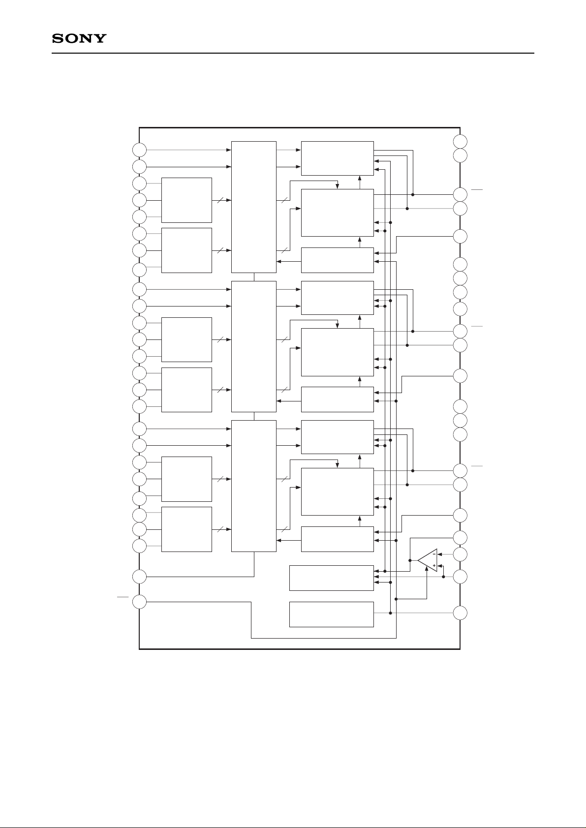
Block Diagram
DECODER
DECODER
DECODER
DECODER
DECODER
DECODER
LATCHES
LATCHES
LATCHES
32
35
34
42
29
41
40
31
30
33
28
39
38
46
45
44
43
27
37
36
48
47
2LSB’S
CURRENT
CELLS
6MSB’S
CURRENT
CELLS
CLOCK
GENERATOR
2LSB’S
CURRENT
CELLS
6MSB’S
CURRENT
CELLS
CLOCK
GENERATOR
2LSB’S
CURRENT
CELLS
6MSB’S
CURRENT
CELLS
CLOCK
GENERATOR
CURRENT CELLS
(FOR FULL SCALE)
BIAS VOLTAGE
GENERATOR
1
2
3
4
5
6
7
8
9
10
11
12
13
14
15
16
17
18
19
20
21
22
23
24
25
26
(LSB) R0
(MSB) R7
(LSB) G0
(MSB) G7
(LSB) B0
B1
B2
B3
B4
B5
B6
(MSB) B7
BLK
CE
R1
R2
R3
R4
R5
R6
G1
G2
G3
G4
G5
G6
DVDD
DVDD
RO
RO
RCK
AV
DD
AVDD
AVDD
AVDD
GO
GO
GCK
AV
SS
DVSS
DVSS
BO
BO
BCK
VG
VREF
IREF
VB
—3—
CXD1178Q
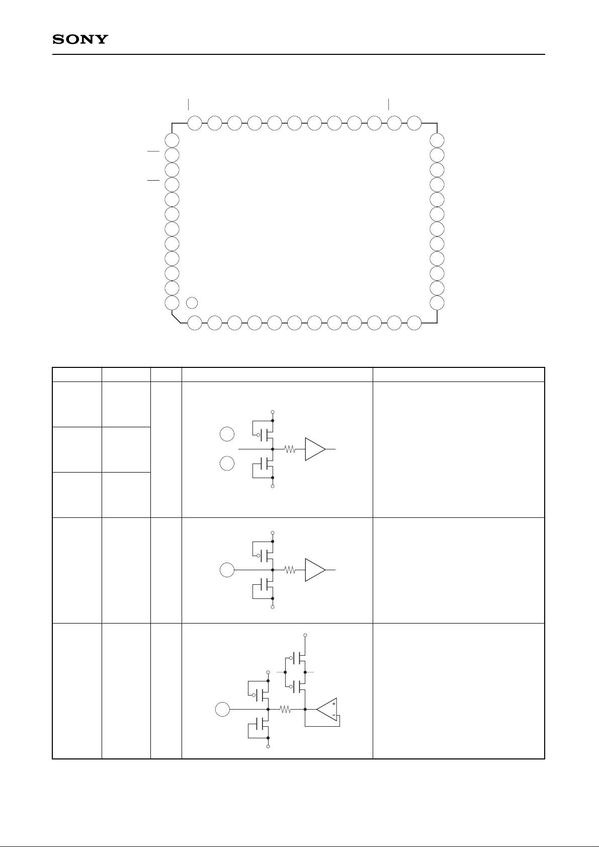
Pin Configuration
R0
R1
R2
R3
R4
R5
R6
R7
G0
G1
G2
G3
B7
B6
B5
B4
B3
B2
B1
B0
G7
G6
G5
G4
BCK
RO
IREF
VREF
AV
SS
VB
DV
SS
DV
SS
GCK
RCK
CE
BLK
RO
GO
GO
BO
BO
VG
AV
DD
AVDD
AVDD
AVDD
DVDD
DVDD
1 2 3 4 5 6 7 8 9
10 11 12
13
14
15
16
17
18
19
20
21
22
23
24
252627282930313233343536
37
38
39
40
41
42
43
44
45
46
47
48
Pin Description and I/O Pins Equivalent Circuit
Pin No. Symbol I/O Equivalent circuit Description
1 to 8
9 to 16
17 to 24
25
32
R0 to R7
G0 to G7
B0 to B7
BLK
VB
I
I
O
1
24
DV
DD
DVSS
to
DVDD
DVSS
25
DVDD
DVSS
32
DVDD
Digital input
R0 (LSB) to R7 (MSB)
G0 (LSB) to G7 (MSB)
B0 (LSB) to B7 (MSB)
Blanking input.
This is synchronized with the clock
input signal for each channel.
No signal at “H” (Output 0 V).
Output condition at “L”.
Connect a capacitor of about 0.1 µF.
—4—
CXD1178Q
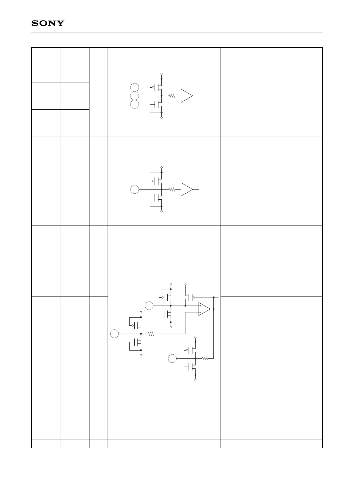
Pin No. Symbol I/O Equivalent circuit Description
27
28
29
30, 31
33
26
35
34
42
43 to 46
RCK
GCK
BCK
DVSS
AVSS
CE
IREF
VREF
VG
AVDD
I
—
—
I
O
I
O
—
DVDD
DVSS
28
27
29
DVDD
DVSS
26
AVDD
AVSS
34
35
AVDD
AVSS
AVDD
AVDD
AVSS
42
Clock input.
Digital GND
Analog GND
Chip enable input.
This is not synchronized with the
clock input signal.
No signal (Output 0 V) at “H” and
minimizes power consumption.
Reference current output.
Connect a resistance 16 times
“16ROUT” that of output resistance
value “ROUT”.
Reference voltage input.
Set full scale output value.
Connect a capacitor of about 0.1 µF.
Analog VDD
—5—
CXD1178Q
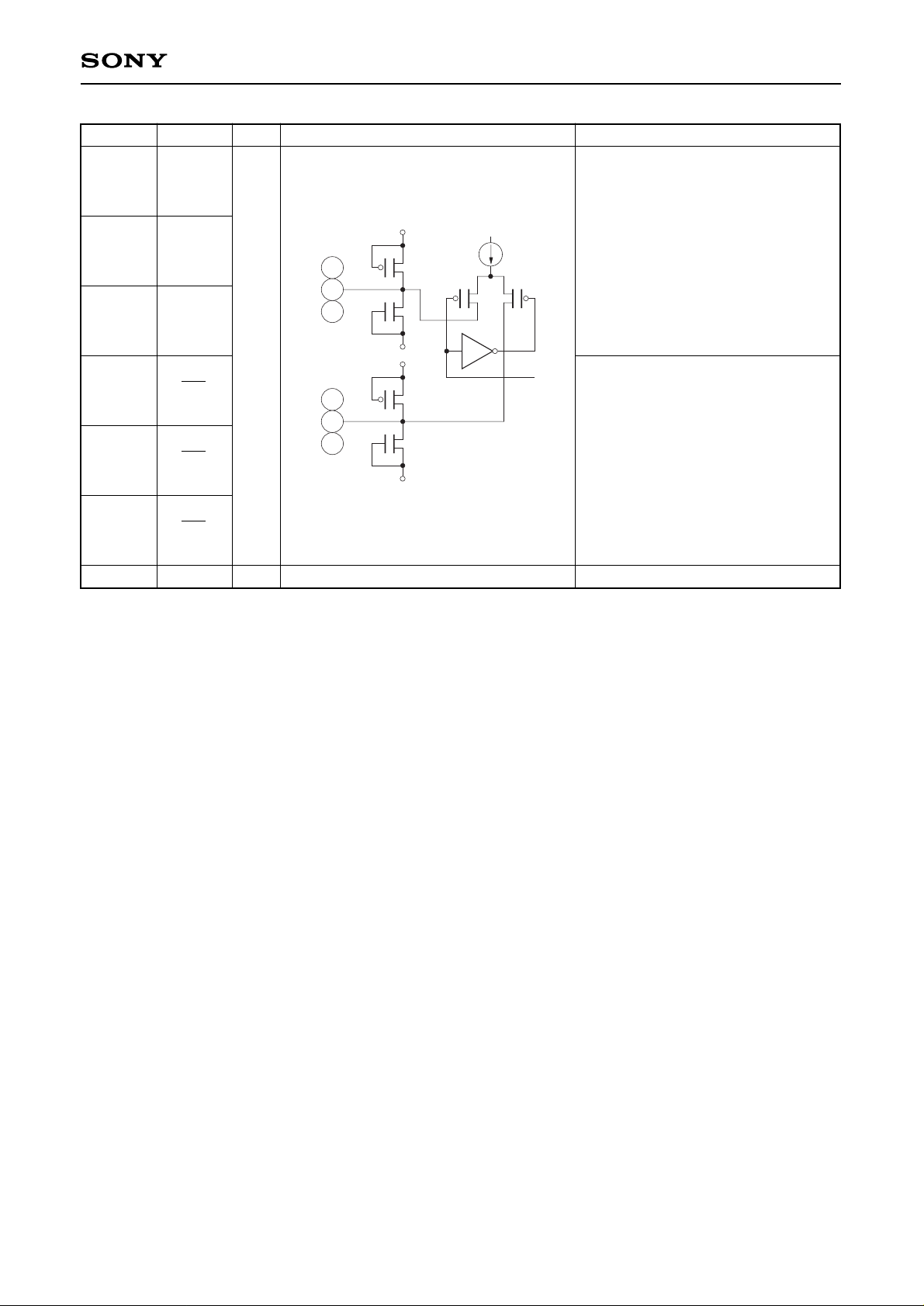
Pin No. Symbol I/O Equivalent circuit Description
37
39
41
36
38
40
47, 48
RO
GO
BO
RO
GO
BO
DVDD
O
—
AVDD
AVSS
41
39
37
AV
DD
AVSS
36
38
40
Current output pins.
Voltage output can be obtained by
connecting a resistance.
Inverted current output.
Normally dropped to analog GND.
Digital VDD
 Loading...