

Sony CXD1176Q Datasheet

—1—
E90167J04-TE
Sony reserves the right to change products and specifications without prior notice. This information does not convey any license by
any implication or otherwise under any patents or other right. Application circuits shown, if any, are typical examples illustrating the
operation of the devices. Sony cannot assume responsibility for any problems arising out of the use of these circuits.
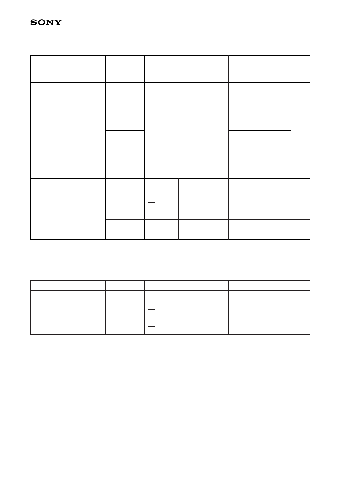
Absolute Maximum Ratings (Ta=25 °C)
• Supply voltage VDD 7V
• Reference voltage
VRT, VRB VDD + 0.5 to VSS – 0.5 V
• Input voltage VIN VDD + 0.5 to VSS – 0.5 V
(Analog)
• Input voltage VI VDD + 0.5 to VSS – 0.5 V
(Digital)
• Output voltage VO VDD + 0.5 to VSS – 0.5 V
(Digital)
• Storage temperature
Tstg –55 to +150 °C
Recommended Operating Conditions
• Supply voltage AVDD, AVSS 4.75 to 5.25 V
DVDD, DVSS
| DVSS – AVSS | 0 to 100 mV
• Reference input voltage
VRB 0 to V
VRT to 2.7 V
• Analog input VIN 1.8Vp-p above
• Clock pulse width
Tpw1, Tpw0 22.5 ns (min) to 1.1 µs (max)
• Operating ambient temperature
Topr –40 to +85 °C
Description
The CXD1176Q is an 8-bit CMOS A/D converter
for video use that features a sync clamp function. The
adoption of a 2 step-parallel method realizes low
power consumption and a maximum conversion
speed of 20MSPS.
Features
• Resolution power: 8-bit ± 1/2LSB (DL)
• Maximum sampling frequency: 20MSPS
• Low power consumption: 60mW (at 20MSPS typ.)
(Reference current excluded)
• Built-in sync type clamp function
• Built-in monostable multivibrator for clamp pulse
generation
• Built-in sync pulse polarity selection function
• Clamp pulse direct input possible
• Built-in clamp ON/OFF function
• Built-in reference voltage self-bias circuit
• Input CMOS compatible
• 3-state TTL compatible output
• Single 5 V power supply
• Low input capacity: 11 pF
• Reference impedance: 330 Ω (typ.)
Applications
TV and VCR digital systems and a wide range of
applications where high-speed A/D conversion is
required.
Structure
Silicon gate CMOS IC
8-bit 20MSPS Video A/D Converter with Clamp Function
32 pin QFP (Plastic)
CXD1176Q

—2—
CXD1176Q
Block Diagram and Pin Configuration
2
3
4
5
6
7
8
10
11
12
9
30
31
32
1
Clock generator
Upper
data
latch
Lower
data
latch
Lower encoder
(4 BIT)
Lower encoder
(4 BIT)
Upper encoder
(4 BIT)
Lower sampling
comparator (4 BIT)
Lower sampling
comparator (4 BIT)
Upper sampling
comparator (4 BIT)
Reference supply
M · M
26
27
29
28
25
24
23
22
21
20
19
18
17
16
15
14
13
DVss
CCP VREFCLE
VRBS
VRB
AVss
AVss
V
IN
AVDD
AVDD
VRT
VRTS
AV
DD
PW
Sync
SEL
OE
DVss
D0 (LSB)
D1
D2
D3
D4
D5
D6
D7 (MSB)
DV
DD
DVDD
CLK
NC
NC

—3—
CXD1176Q
Pin Description
Pin No. Symbol Equivalent circuit Description
1 to 8
D0 to D7
CLK
SEL
Sync
D0 (LSB) to D7 (MSB) output
Clock input
When SEL is at low, with the falling
edge of Pin 14 (sync) as trigger, the
monostable multivibrator generates
clamp pulses.
When SEL is at high, with the rising
edge of Pin 14 (sync) as trigger, it
generates clamp pulses.
Trigger pulse input to the monostable
multivibrator.
Trigger polarity can be selected
through Pin 13 (SEL).
12
13
14
Di
DVDD
DVSS
12
DVDD
DVSS
14
9, 32
NC
NC pin
10, 11
DVDD
Digital +5 V
DVDD
DVSS
13

—4—
CXD1176Q
15
PW
18
VRT
24
VRB
21 VIN
25
VRBS
17
VRTS
When a clamp pulse is generated at
the monostable multivibrator, the
pulse width is determined by the
external R and C.
When the clamp pulse is directly
input, it is input to Pin 15 (PW). The
signal voltage of the low period is
clamped. (Here, Pin 14 (sync) is fixed
to either low or high.)
When shorted with VRT, generates
approx. +2.6 V.
Reference voltage (top)
Reference voltage (bottom)
Analog input
When shorted with VRB, generates
approx. +0.5 V.
Pin No. Symbol
Equivalent circuit Description
22, 23
AVSS
16, 19, 20 AVDD
17
AV
DD
18
24
AV
DD
AVSS
21
AV
DD
AVSS
25
AVSS
Analog +5 V
Analog ground
15
DV
DD
DVSS

—5—
CXD1176Q
Pin No. Symbol Equivalent circuit Description
26 VREF
CCP
CLE
OE
Clamp reference voltage input.
Clamps to provide a clamp period
input signal equal to the reference
voltage.
Integrates the voltage for clamp
control.
CCP and VIN voltage changes are in
positive phase.
When CLE is at low, clamp function is
activated.
When CLE is at high, clamp function
is OFF and only the usual A/D
converter function is active.
By connecting CLE pin to DVDD via a
several hundred Ω resistance, the
clamp pulse can be tested.
When OE is at low, Data is output.
When OE ia at high, D0 to D7 pins
turn to high impedance.
27
29
30
26
AV
DD
AVSS
27
AV
DD
AVSS
29
CLAMP
PULSE
DV
DD
DVSS
30
DV
DD
DVSS
28, 31
DVSS
Digital ground.

—6—
CXD1176Q
Digital Output
Correspondence between the analog input voltage and the digital output code is indicated in the chart below.
tr = 4.5ns tf = 4.5ns
2.5V
tPLZ
tPHZ
10%
90%
tPZH
1.3V
1.3V
tPZL
10%
90%
5V
0V
V
OH
VOL (≠ DVSS)
V
OH (≠ DVDD)
V
OL
OE input
Output 1
Output 2
Input signal
voltage
Step
Digital output code
MSB LSB
VRT
.
.
.
.
.
.
.
.
.
.
.
.
VRB
0
.
.
.
127
128
.
.
.
255
1 1 1 1 1 1 1 1
.
.
.
1 0 0 0 0 0 0 0
0 1 1 1 1 1 1 1
.
.
.
0 0 0 0 0 0 0 0
Timing Chart. I
Timing Chart. II
Clock
Analog input
Data output
TPW1 TPW0
N
N – 3 N – 2 N – 1 N N + 1
N + 1
N + 2
N + 3
N + 4
Td = 18ns
: Points where analog signals are sampled.

—7—
CXD1176Q
Electrical Characteristics
Analog characteristics (Fc = 20 MSPS, VDD = 5 V, VRB = 0.5 V, VRT = 2.5 V, Ta = 25 °C)
Conversion speed
Analog input band width
(–1dB)
Offset voltage
∗1
Integral non-linearity error
Differential non-linearity erro
r
Differential gain error
Differential phase error
Aperture jitter
Sampling delay
Clamp offset voltage
∗2
Clamp pulse width
(Sync pin input)
Clamp pulse delay
Fc
BW
EOT
EOB
EL
ED
DG
DP
taj
tsd
Eoc
tcpw
tcpd
0.5
–60
+20
0
–50
1.75
VDD = 4.75 to 5.25 V
Ta = –40 to +85 °C
VIN = 0.5 to 2.5 V
fIN = 1 kHz ramp
Envelope
Potential difference to VRT
Potential difference to VRB
End point
NTSC 40 IRE mod ramp
Fc = 14.3 MSPS
VIN = DC,
PWS = 3 µs
C = 100 pF,
R = 130 kΩ (15 PIN)
18
–40
+40
+0.5
±0.3
1.0
0.5
30
4
+20
–30
2.75
25
20
–20
+60
+1.3
±0.5
+40
–10
3.75
MSPS
MHz
mV
LSB
%
deg
ps
ns
mV
µs
ns
Item Symbol Conditions Min. Typ. Max. Unit
VREF = 0.5 V
VREF = 2.5 V
∗1
The offset voltage EOB is a potential difference between VRB and a point of position where the voltage
drops equivalent to 1/2 LSB of the voltage when the output data changes from “00000000” to “00000001”.
EOT is a potential difference between VRT and a potential of point where the voltage rises equivalent to
1/2LSB of the voltage when the output data changes from “11111111” to “11111110”.
∗2
Clamp offset voltage varies individually. When using with R, G, B 3 channels, color sliding may be
generated.
—8—
CXD1176Q
DC characteristics
(Fc = 20 MSPS, VDD = 5 V, VRB = 0.5 V, VRT = 2.5 V, Ta = 25 °C)
Supply current
Reference pin current
Analog input capacitance
Reference resistance
(VRT to VRB)
Self-bias I
Self-bias II
Digital input voltage
Digital input current
Digital output current
IDD
IREF
CIN
RREF
VRB1
VRT1 to VRB1
VRT2
VIH
VIL
IIH
IIL
IOH
IOL
IOZH
IOZL
4.5
230
0.48
1.96
4.0
–1.1
3.7
Fc = 20 MSPS
NTSC ramp wave input
VIN = 1.5 V + 0.07 Vrms
VRB and VRBS are shorted
VRT and VRTS are shorted
VRB = AGND
VRT and VRTS are shorted
VDD = 4.75 to 5.25 V
Ta = –40 to +85 °C
VDD = max
OE = VSS
VDD = min
OE = VDD
VDD = max
12
6.6
11
300
0.52
2.08
2.32
18
8.7
450
0.56
2.22
1.0
5
5
16
16
mA
mA
pF
Ω
V
V
V
µA
mA
µA
Item Conditions Min. Typ. Max. Unit
Timing
(Fc = 20 MSPS, VDD = 4.75 to 5.25 V, VRB = 0.5 V, VRT = 2.5 V, Ta = –40 to +85 °C)
Output data delay
Tri-state output
enable time
Tri-state output
disable time
TDL
tPZH
tPZL
tPHZ
tPLZ
2.5
8
with TTL 1 gate and 10pF load
RL = 1kΩ, CL = 20 pF
OE = 3 V → 0 V
RL = 1 kΩ, CL = 20 pF
OE = 0 V → 3 V
18
6
18
30
10
30
ns
ns
ns
Item Symbol Conditions Min. Typ. Max. Unit
VIH = VDD
VIL = 0V
VOH = VDD – 0.5 V
VOL = 0.4V
VOH = VDD
VOL = 0V
 Loading...