

Sony CXD1172AP, CXD1172AM Datasheet

CXD1172AM/AP
6-bit 20MSPS Video A/D Converter (CMOS)
Description
CXD1172AM/AP is a 6-bit CMOS A/D converter for
video use. The adoption of a 2-step parallel system
achieves low consumption at a maximum conversion
speed of 20MSPS minimum, 35MSPS typical.
Features
• Resolution: 6-bit ± 1/2LSB
• Max. sampling frequency: 20MSPS
• Low power consumption: 40mW (at 20MSPS typ.)
(Reference current excluded)
• Built-in sampling and hold circuit.
• 3-state TTL compatible output.
• Power supply: 5V single
• Low input capacitance: 4pF
• Reference impedance: 250Ω (typ.)
Applications
TV, VCR digital systems and a wide range of fields
where high speed A/D conversion is required.
Structure
Silicon gate CMOS monolithic IC
CXD1172AM
16 pin SOP (Plastic)
Absolute Maximum Ratings (Ta = 25°C)
• Supply voltage VDD 7V
• Reference voltage
VRT, VRB VDD + 0.5 to VSS – 0.5 V
• Input voltage VIN VDD + 0.5 to VSS – 0.5 V
(Analog)
• Input voltage VCLK VDD + 0.5 to VSS – 0.5 V
(Digital)
• Output voltage VOH, VOL VDD + 0.5 to VSS – 0.5 V
(Digital)
• Storage temperature
Tstg –55 to +150 °C
Recommended Operating Conditions
• Supply voltage AVDD, AVSS 4.75 to 5.25 V
DVDD, DVSS 4.75 to 5.25 V
• Reference input voltage
VRB 0 to 4.1 V
VRT 0.9 to 5.0 V
VRT – VRB 0.9 to AVDD V
• Analog input voltage
VIN VRB to VRT V
• Clock pulse width
TPW1, TPW0 23ns (min.) to 1.1µs (max.)
• Operating temperature
Topr –20 to +75 °C
CXD1172AP
16 pin DIP (Plastic)
Sony reserves the right to change products and specifications without prior notice. This information does not convey any license by
any implication or otherwise under any patents or other right. Application circuits shown, if any, are typical examples illustrating the
operation of the devices. Sony cannot assume responsibility for any problems arising out of the use of these circuits.
– 1 –
E89320C78-PS
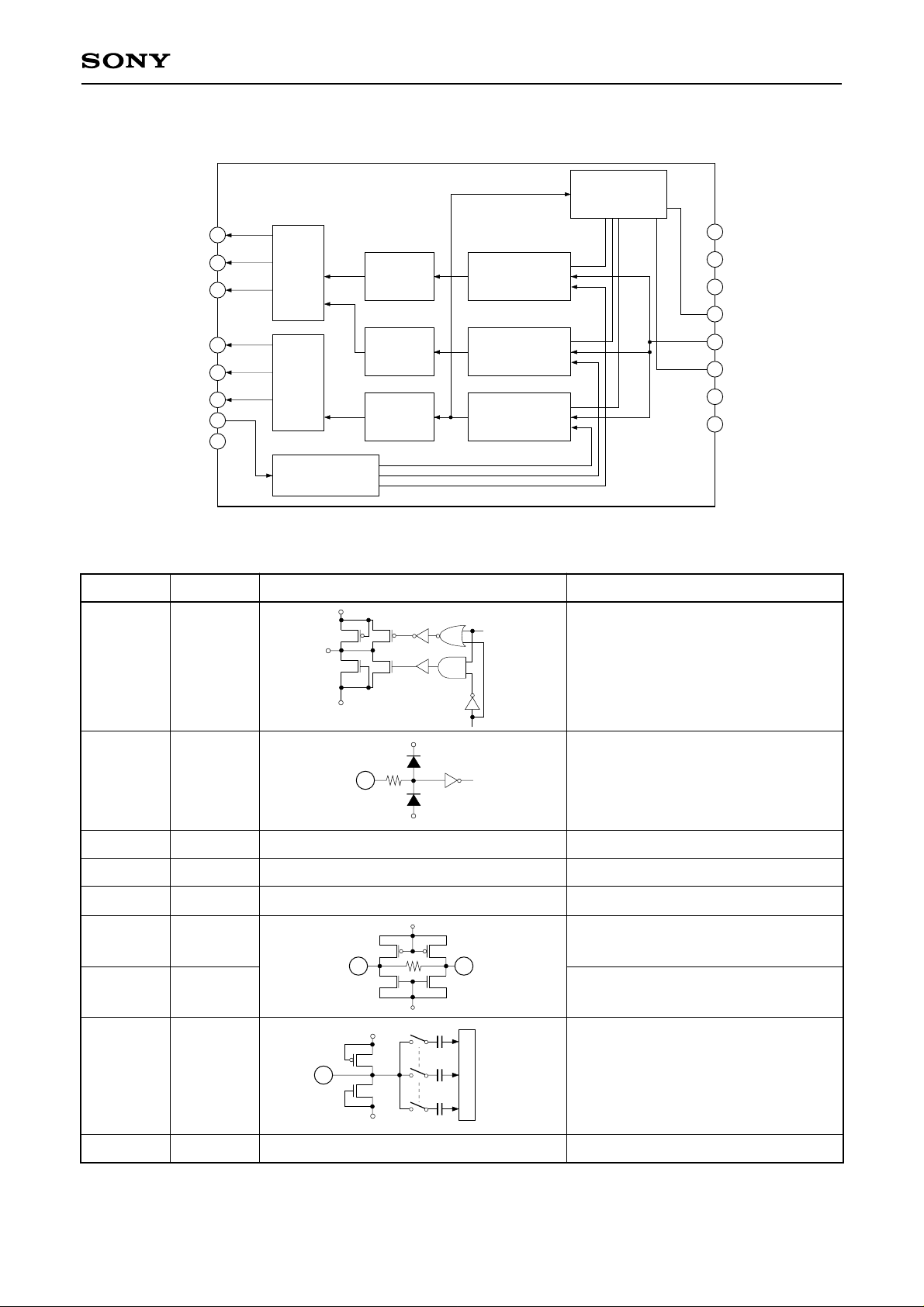
Block Diagram and Pin Configuration
1
D
0
2
CLK
DVSS
D1
3
D2
4
3
D
5
D4
6
D5
7
8
Lower data
latchs
Upper data
latchs
Clook generator
Lower encoder
(3BIT)
Lower encoder
(3BIT)
Upper encoder
(3BIT)
Lower
Sampling comparators
(3BIT)
Lower
Sampling comparators
(3BIT)
Upper
Sampling comparators
(3BIT)
Reference voltage
CXD1172AM/AP
16
AV
SS
15
DVDD
14
AVDD
13
VRB
12
IN
V
11
VRT
10
AVDD
9
DVDD
Pln Description and Equivalent Circuits
No. Symbol Equivalent Circuit
Di
1 to 6
7
8
9, 15
10, 14
11
13
D0 to D5
CLK
DVSS
DVDD
AVDD
VRT
VRB
11
DVDD
7
DV
SS
AV
DD
AVSS
AVDD
Description
D0 (LSB) to D5 (MSB) output
Clock input
Digital GND
Digital +5V
Analog +5V
Reference voltage (Top)
13
Reference voltage (Bottom)
12
16
VIN
AVSS
12
Analog input
AVSS
Analog GND
– 2 –
CXD1172AM/AP
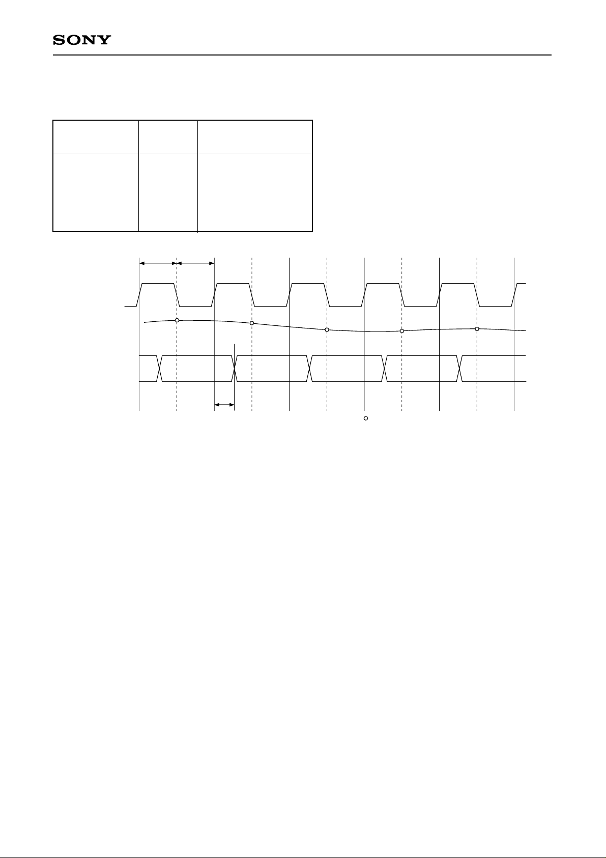
Digital Output
Compatibility between Analog input voltage and the digital output code is indicated in the chart below.
Input signal
voltage
VRT
..............
VRB
Clock
Analog input
Data output
Step
0
......
31
32
63
TPW1 TPW0
N
N – 3 N – 2 N – 1 N N + 1
Digital output code
MSB LSB
1 1 1 1 1 1
......
1 0 0 0 0 0
0 1 1 1 1 1
0 0 0 0 0 0
N + 1
Td = 18ns
N + 2 N + 3
: Point for analog signal sampling.
N + 4
Timing Chart 1
– 3 –
CXD1172AM/AP
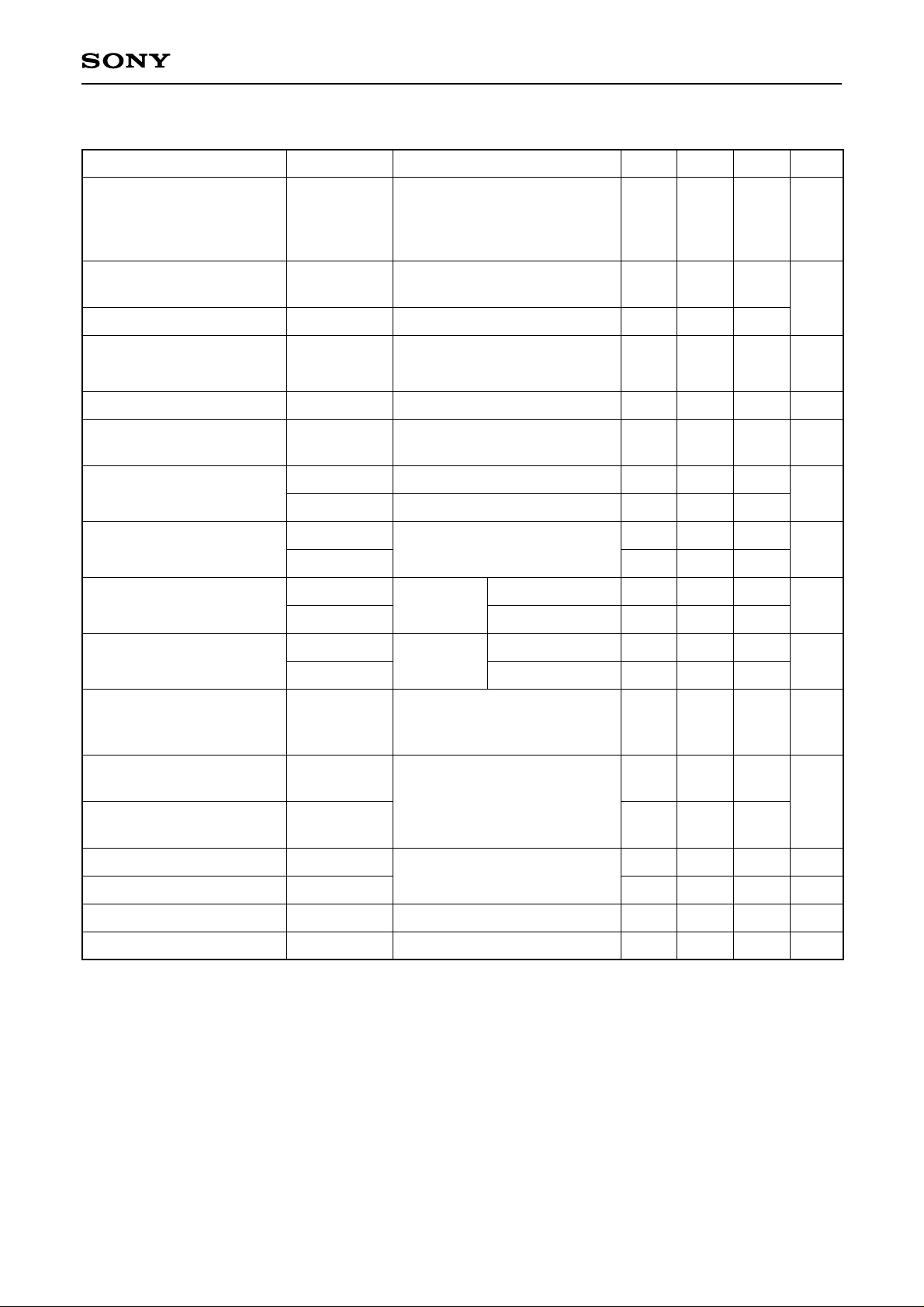
Electrical Characteristics (VDD = 5V, VRB = 1.0V, VRT = 2.0V, Ta = 25°C)
Item Symbol Conditions Min. Typ. Max. Unit
VDD = 4.75 to 5.25V
Conversion speed
Fc
Ta = –20 to +75°C
VIN = 1.0 to 2.0V
0.5
20
MSPS
fIN = 1kHz ramp
Supply current
Reference pin current
Analog input band width
(–1dB)
Analog input capacitance
Reference resistance
(VRT to VRB)
Offset voltage
∗1
Digital input voltage
Digital input current
Digital output current
Output data delay
IDD
IREF
BW
CIN
RREF
EOT
EOB
VIH
VIL
IIH
IIL
IOH
IOL
TDL
Fc = 20MSPS
NTSC ramp wave input
Envelope
VIN = 1.5V + 0.07Vrms
Potential difference to VRT
Potential difference to VRB
VDD = 4.75 to 5.25V
Ta = –20 to +75°C
VIH = VDD
VDD = max.
VIL = 0V
VOH = VDD + 0.5V
VDD = min.
VOL = 0.4V
With TTL 1 gate and 10pF load
Ta = –20 to +75°C
VDD = 4.75 to 5.25V
3
175
0
15
4.0
–1.1
3.7
7
4
18
4
250
–20
35
18
12
5.7
325
–40
55
1.0
5
5
30
mA
MHz
pF
Ω
mV
V
µA
mA
ns
Integral non-linearity error
EL
±0.3
±0.5
End point
Differential non-linearity
error
Differential gain error
Differential phase error
Aperture jitter
Sampling delay
∗1
The offset voltage EOB is a potential difference between VRB and a point of position where the voltage
ED
DG
DP
Taj
Tsd
NTSC 40 IRE mod ramp
Fc = 14.3MSPS
±0.3
1.0
1.0
40
4
±0.5
drops equivalent to 1/2 LSB of the voltage when the output data changes from "00000000" to "00000001".
EOT is a potential difference between VRT and a potential of point where the voltage rises equivalent to
1/2 LSB of the voltage when the output data changes from "11111111" to "11111110".
– 4 –
LSB
%
deg
ps
ns
 Loading...