

Sony CXD1171M Datasheet

—1—
E89X38F01
Sony reserves the right to change products and specifications without prior notice. This information does not convey any license by
any implication or otherwise under any patents or other right. Application circuits shown, if any, are typical examples illustrating the
operation of the devices. Sony cannot assume responsibility for any problems arising out of the use of these circuits.
Absolute Maximum Ratings (Ta=25 °C)
• Supply voltage AVDD, DVDD 7V
• Input voltage (All pins)
VIN VDD +0.5 to VSS –0.5 V
• Output current IOUT 15 mA
• Storage temperature
Tstg –55 to +150 °C
Recommended Operating Conditions
• Supply voltage AVDD, AVSS 4.75 to 5.25 V
DVDD, DVSS 4.75 to 5.25 V
• Reference input voltage
VREF 2.0 V
• Clock pulse width
Tpw1,Tpw0 11.2 ns (min) to 1.1 µs (max)
• Operating temperature
Topr –40 to +85 °C
Description
The CXD1171M is a 8-bit 40 MHz high speed D/A
converter. The adoption of a current output system
reduces power consumption to 80 mW (200 Ω load
at 2 Vp-p output).
This IC is suitable for digital TV and graphic
display applications.
Features
• Resolution 8-bit
• Max. conversion speed 40MSPS
• Non linearity error within ±0.25 LSB
• Low glitch noise
• TTL CMOS compatible input
• +5 V single power supply
• Low power consumption 80 mW
(200 Ω load at 2 Vp-p output)
Function
8-bit 40 MHz D/A converter
Structure
Silicon gate CMOS IC
8-bit 40MSPS High Speed D/A Converter
24 pin SOP (Plastic)
CXD1171M

—2—
CXD1171M
Block Diagram and Pin Configuration
6MSB'S
CURRENT
CELLS
LATCHES
DECODER
19
20
21
22
23
24
CLOCK
GENERATOR
2
3
4
5
6
7
8
9
10
11
12
13
14
15
16
17
18
1
CURRENT CELLS
(FOR FULL SCALE)
BIAS VOLTAGE
GENERATOR
DECODER
2LSB'S
CURRENT
CELLS
(LSB) D0
D1
D2
D3
D4
D5
D6
(MSB) D7
BLK
DV
SS
VB
CLK
DV
DD
DVDD
AVDD
IO
IO
AV
DD
AVDD
VG
VREF
IREF
AV
SS
DVSS
—3—
CXD1171M
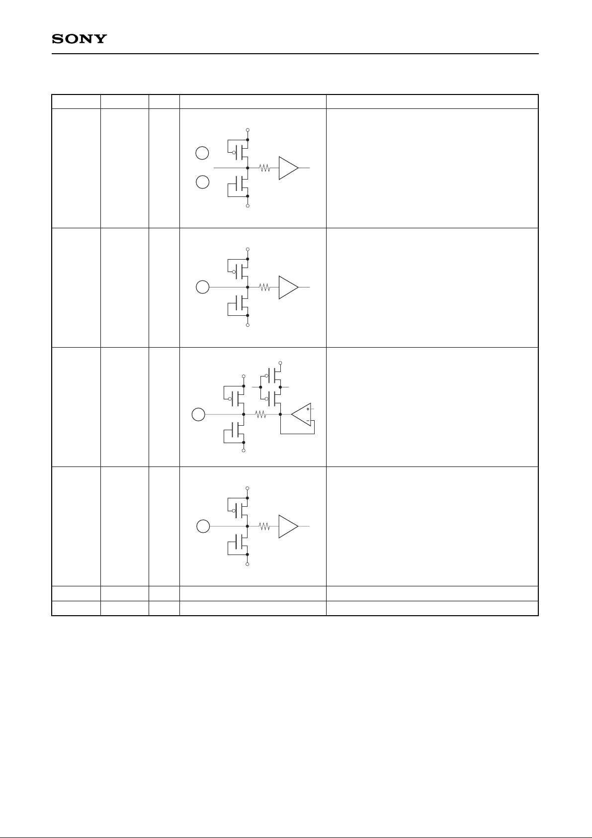
Pin Description and I/O Pins Equivalent Circuit
1 to 8
9
11
12
10, 13
14
D0 to D7
BLK
VB
CLK
DVSS
AVSS
I
I
O
I
—
—
No. Symbol I/O Equivalent circuit Description
DVDD
DVSS
to
8
1
DVDD
DVSS
9
DVDD
DVSS
DVDD
11
DVDD
DVSS
12
Digital input.
D0 (LSB) to D7 (MSB)
D0 and D1 have a pull-down resistor.
Blanking input.
This is synchronized with the clock signal.
No signal at “H” (Output 0 V).
Output condition at “L”.
Connect a capacitor of about 0.1 µF.
Clock input.
Digital ground.
Analog ground.

—4—
CXD1171M
15
16
17
18, 19, 22
20
21
23, 24
IREF
VREF
VG
AVDD
IO
IO
DVDD
O
I
O
—
O
—
No. Symbol I/O Equivalent circuit Description
AVSS
AVSS
AVDD
AVDD
AVSS
AVDD
AVDD
15
16
17
AVDD
AVSS
AVDD
AVSS
20
21
Set full-scale output value.
Connect a capacitor of about 0.1 µF.
Analog power supply.
Current output.
Voltage output can be obtained by connecting
a resistance.
Inverted current output.
Normally connected to analog GND.
Digital power supply.
Connect a resistor “RIR” 16 times against the
output resistance value “ROUT” connected to
Pin 20 (IO).
 Loading...