

Sony CXD1170M Datasheet
6-bit 40MSPS High Speed D/A Converter
For the availability of this product, please contact the sales office.
Description
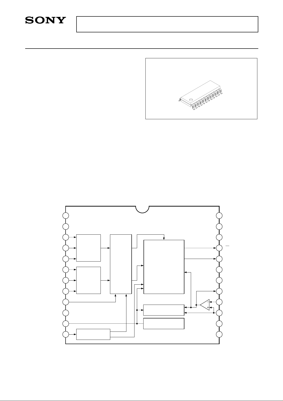
The CXD1170M is a 6-bit 40MHz high speed D/A
converter. The adoption of a current output system
reduces power consumption to 80mW (200Ω load at
2Vp-p output).
This IC is suitable for digital TV and graphic
display applications.
Features
• Resolution 6-bit
• Max. conversion speed 40MSPS
• Non linearity error within ±0.1LSB
• Low glitch noise
• TTL CMOS compatible input
• +5V single power supply
• Low power consumption 80mW
(200Ω load at 2Vp-p output)
Structure
Silicon gate CMOS IC
Function
6-bit 40MHz D/A converter
CXD1170M
24 pin SOP (Plastic)
Block Diagram and Pin Configuration
NC
1
NC
2
(LSB) D0
BLK
DV
CLK
D1
D2
D3
D4
D5
SS
VB
10
12
11
3
4
5
6
7
8
9
DECODER
DECODER
CLOCK
GENERATOR
LATCHES
CURRENT
CELLS
CURRENT CELLS
(FOR FULL SCALE)
BIAS VOLTAGE
GENERATOR
23
22
21
20
19
18
17
16
15
14
13
24
DD
DV
DD
DV
AVDD
IO
IO
AVDD
AVDD
VG
VREF
IREF
AV
SS
DVSS
Sony reserves the right to change products and specifications without prior notice. This information does not convey any license by
any implication or otherwise under any patents or other right. Application circuits shown, if any, are typical examples illustrating the
operation of the devices. Sony cannot assume responsibility for any problems arising out of the use of these circuits.
– 1 –
E89X37B6X-PS
Absolute Maximum Ratings (Ta = 25°C)
• Supply voltage VDD 7V
•Input voltage VIN VDD to VSS V
• Output current IOUT 15 mA
• Storage temperature Tstg –55 to +150 °C
Recommended Operating Conditions
• Supply voltage AVDD, AVSS 4.75 to 5.25 V
DVDD, DVSS 4.75 to 5.25 V
• Reference input voltage VREF 2.0 V
• Clock pulse width Tpw1 12.5 (Min) ns
Tpw0 12.5 (Min) ns
• Operating temperature Topr –20 to +75 °C
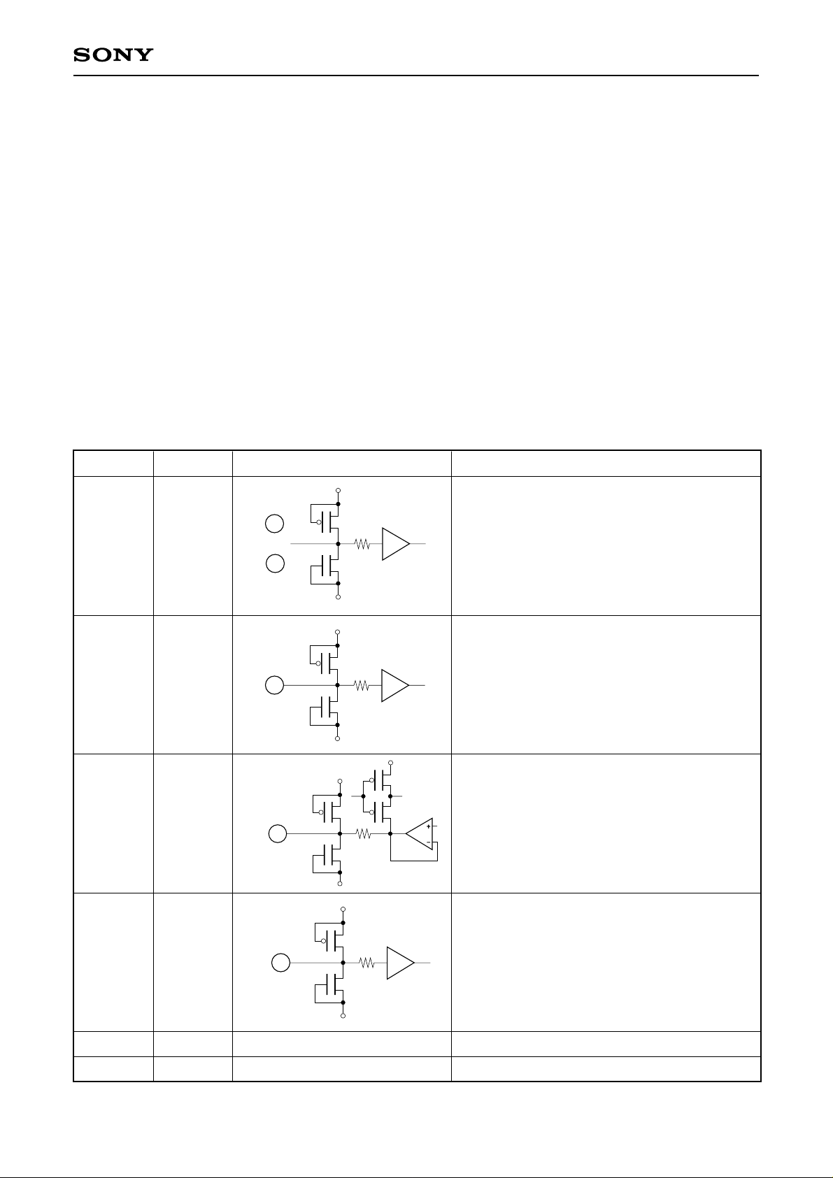
Pin Description and I/O Pins Equivalent Circuit
CXD1170M
No. Symbol Equivalent circuit Description
DVDD
3
3 to 8 D0 to D5 Digital input
to
8
DVSS
DVDD
Blanking pin
9 BLK
9
No signal at "H" (Output 0V)
Output condition at "L"
DVSS
DVDD
DVDD
11 VB Connect a capacitor of about 0.1µF
11
DVSS
DVDD
Clock pin
12 CLK
12
Moreover all input pins are TTL-CMOS
compatible
DVSS
10, 13 DVSS Digital GND
14 AVSS Analog GND
– 2 –
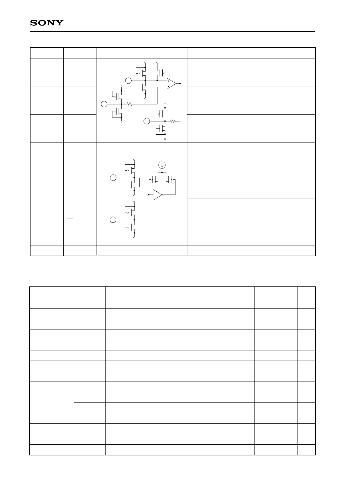
No. Symbol Equivalent circuit Description
AVDD
15 IREF
15
AVDD
AVDD
Connect a resistance 16 times "16R" that of
output resistance value "R"
CXD1170M
16 VREF Set full scale output value
16
AVSS
AVSS
AVDD
17
17 VG Connect a capacitor of about 0.1µF
AVSS
18, 19, 22 AVDD Analog VDD
AVDD
Current output pin
20 IO
20
Voltage output can be obtained by connecting
a resistance
AVSS
AVDD
21 IO
21
AVSS
Inverted current output pin
Normally dropped to analog GND
23, 24 DVDD Digital VDD
Eleoctrical Characteristics (fCLK = 40MHz, VDD = 5V, ROUT = 200Ω, VREF = 2.0V, Ta = 25°C)
Item
Resolution
Maximum conversion speed
Minimum conversion speed
Linearity error
Differential linear error
Full scale output voltage
Full scale output current
Offset output voltage
Power supply current
Digital
input current
High level
Low level
Setup time
Hold time
Propagation delay time
Symbol
n
fMAX
fMIN
EL
ED
VFS
IFS
VOS
IDD
IIH
IIL
tS
tH
tPD
14.3MHz, at COLOR BAR DATA input
Measurement conditions
Min.
0.5
–0.3
–0.1
1.85
13
–5
5
10
Typ.
6
1.95
10
14.5
10
Max.
40
0.5
0.1
2.05
15
1
16
5
Unit
bit
MSPS
MHz
LSB
LSB
V
mA
mV
mA
µA
µA
ns
ns
ns
Glitch energy
GE
ROUT = 75Ω
– 3 –
30
pV-s
 Loading...