Sony CXB1810FN Datasheet

CXB1810FN
Post Amplifier for Optical Fiber Communication Receiver
Description
The CXB1810FN achieves 2R optical fiber
communication receiver functions (Reshaping and
Regenerating) on a single chip.
This IC is equipped with a signal detection function,
and outputs at TTL level.
Features
• Auto-offset canceler circuit
• Signal interruption alarm output
• Single 3.3V or 5.0V power supply
Applications
SONET/SDH
Absolute Maximum Ratings
• Supply voltage VCC – VEE –0.3 to +6.0 V
• Input voltage difference | VD – VDN | 2.5 V
• ECL/TTL output current (Continuous) 50 mA
(Surge) 70 mA
• Storage temperature Tj –65 to +150 °C
Recommended Operating Conditions
• Supply voltage VCC – VEE 3.14 to 5.25 V
• Termination voltage (for Q/QB) Vt1 VCC – 1.8 to Vcc – 2.2 V
• Termination resistance (for Q/QB) Rt 46 to 56 Ω
• Operating temperature Ta –40 to +85 °C
– 1 –
E99801D26-PS
Sony reserves the right to change products and specifications without prior notice. This information does not convey any license by
any implication or otherwise under any patents or other right. Application circuits shown, if any, are typical examples illustrating the
operation of the devices. Sony cannot assume responsibility for any problems arising out of the use of these circuits.
16 pin HSOF (plastic)

– 2 –
CXB1810FN
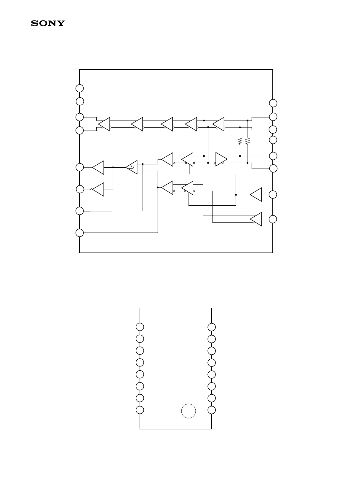
Block Diagram
Q
D
Vcc
V
EE
DB
CAP1
CAP1B
SW
DOWN
QB
V
EEO
VccO
CAP3
CAP2
SDC
SDCB
1
2
3
4
5
6
7
8
9
10
11
12
13
14
15
16
Pin Configuration
1
2
3
4
5
6
7
8
9
10
11
12
13
14
15
16
CAP2
CAP3
SDCB
SDC
QB
Q
VCCO
VEEO
DOWN
SW
CAP1B
CAP1
VEE
DB
D
VCC

– 3 –
CXB1810FN
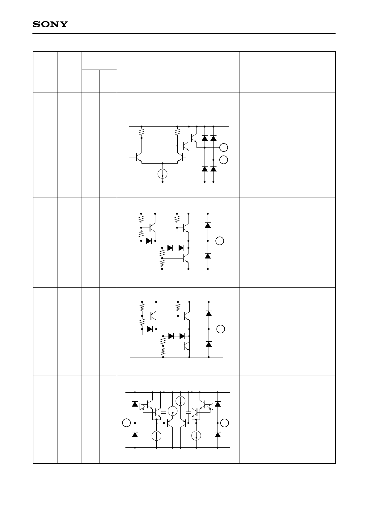
Pin
No.
Symbol
Typical pin
voltage (V)
DC
AC
Equivalent circuit
Description
3
4
V
CCO
VEEO
1
V
EEO
0
Ground for data output circuit.
2
VccO
3.3 or
5.0
Positive power supply for data
output circuit.
5
V
CC
VEE
3
4
Q
QB
1.7
to
2.4
or
3.4
to
4.1
Data outputs.
5
SDC
0.2
to
2.9
or
0.2
to
4.7
Signal detection output (TTL).
The SDC output is driven to low
level while signal interruption is
detected.
Pin Description
6
V
CC
VEE
8
7
V
CC
VEE
6
SDCB
0.2
to
2.9
or
0.2
to
4.7
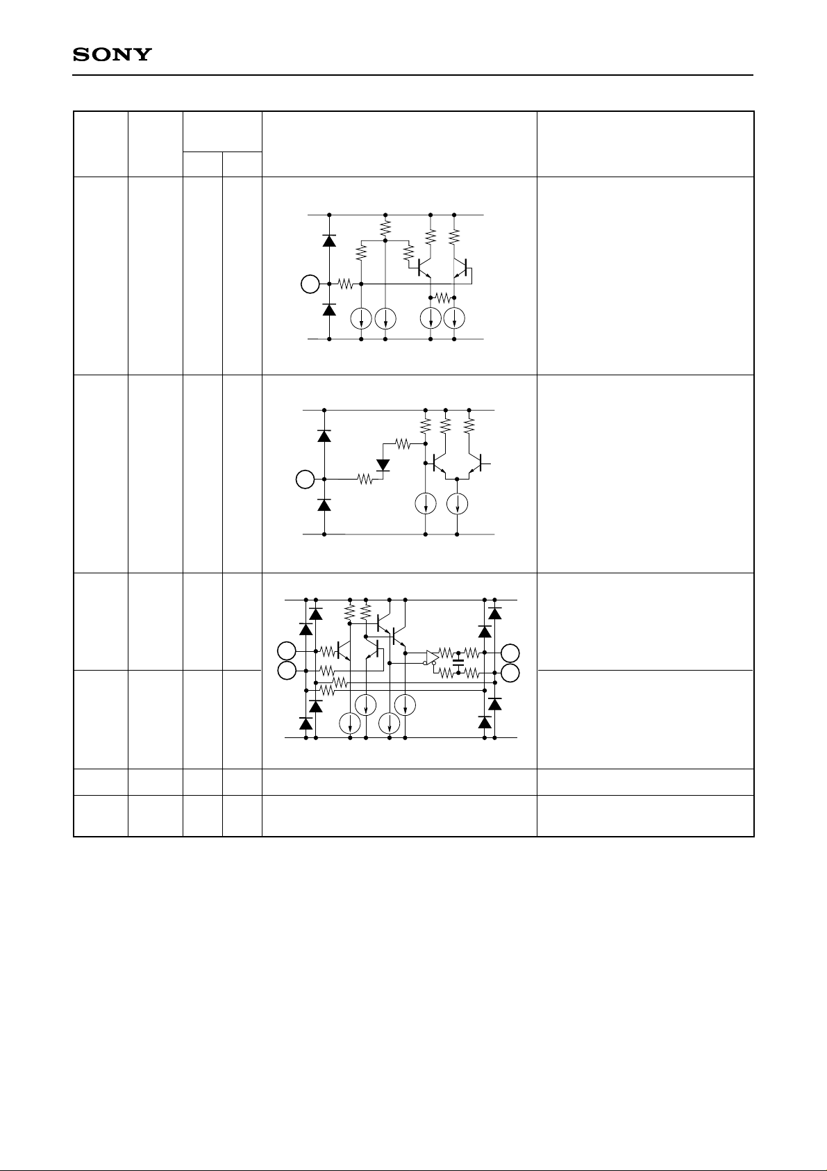
Signal detection output (TTL).
The SDCB output is driven to
high level while signal
interruption is detected.
7
8
CAP3
CAP2
1.6 or
3.3
1.3
to
1.8
or
3.0
to
3.5
Connect a peak hold capacitor
for the signal detection circuit.
470pF (typ.)

– 4 –
CXB1810FN
9
V
CC
VEE
10
V
CC
VEE
Pin
No.
Symbol
Typical pin
voltage (V)
DC
AC
Equivalent circuit
Description
9
DOWN
2.4 or
4.1
Connect a resistor between this
pin and the V
CC pin to decrease
the signal detection level from
the default value.
10
SW
Switches the maximum
identification voltage amplitude.
This pin is set to 50mVp-p
(single ended) when open or high
level, or to 15mVp-p (single
ended) when low level.
Setting to low level is
recommended when using a
resistor of 510Ω or less between
the V
CC and DOWN pins.
11
12
CAP1B
CAP1
14
15
DB
D
2.2 or
3.9
Connect an external capacitor
between these pins.
0.022µF (typ.)
Data inputs.
13
V
EE
0
Ground.
16
V
CC
3.3 or
5.0
Positive power supply.
11
12
14
15
V
CC
VEE

– 5 –
CXB1810FN
Electrical Characteristics
DC Characteristics (VCC = 3.14 to 5.25V, Ta = –40 to +85°C, unless otherwise specified)
Item
Q/QB high output voltage
Q/QB low output voltage
Q/QB output amplitude
SDC/SDCB high output voltage
SDC/SDCB low output voltage
SW high input voltage
SW low input voltage
Maximum input voltage
amplitude
D/DB input resistance
Supply current
VOH1
VOL1
Vp
VOHT
VOLT
VIHT
VILT
Vmax
Rin
ICC
51Ω terminated to V
CC – 2V
51Ω terminated to VCC – 2V
51Ω terminated to VCC – 2V
IOH = –0.2mA
IOL = 2.1mA
During single-phase input
All outputs open
VCC – 1100
VCC – 1800
500
2.4
VCC – 0.3
VEE
1000
33 50
40
VCC – 650
VCC – 1300
1000
0.5
VCC
VEE + 0.3
69
55
mV
mV
mVp-p
V
V
V
V
mVp-p
Ω
mA
Symbol Min. Typ. Max. UnitConditions
Item
Limiting amplifier gain
Signal detection threshold voltage
Signal detection hysteresis width
Signal detection response assert time
∗
1
Signal detection response deassert time
∗1
Q/QB rise time (20 to 80%)
Q/QB fall time (20 to 80%)
GL
Vth
∆P
Tas
Tdas
TR
TF
During single ended input
51Ω terminated to VCC – 2V
51Ω terminated to VCC – 2V
45
3
0
2.3
34
6
130
110
8
100
100
dB
mVp-p
dB
µs
µs
ps
ps
Symbol Min. Typ. Max. UnitConditions
AC Characteristics (VCC = 3.14 to 5.25V, Ta = –40 to +85°C, unless otherwise specified)
∗
1
Data = PN23 – 1 pattern, 100mVp-p single ended, Rd = open, CAP2/CAP3 = 470pF

– 6 –
CXB1810FN
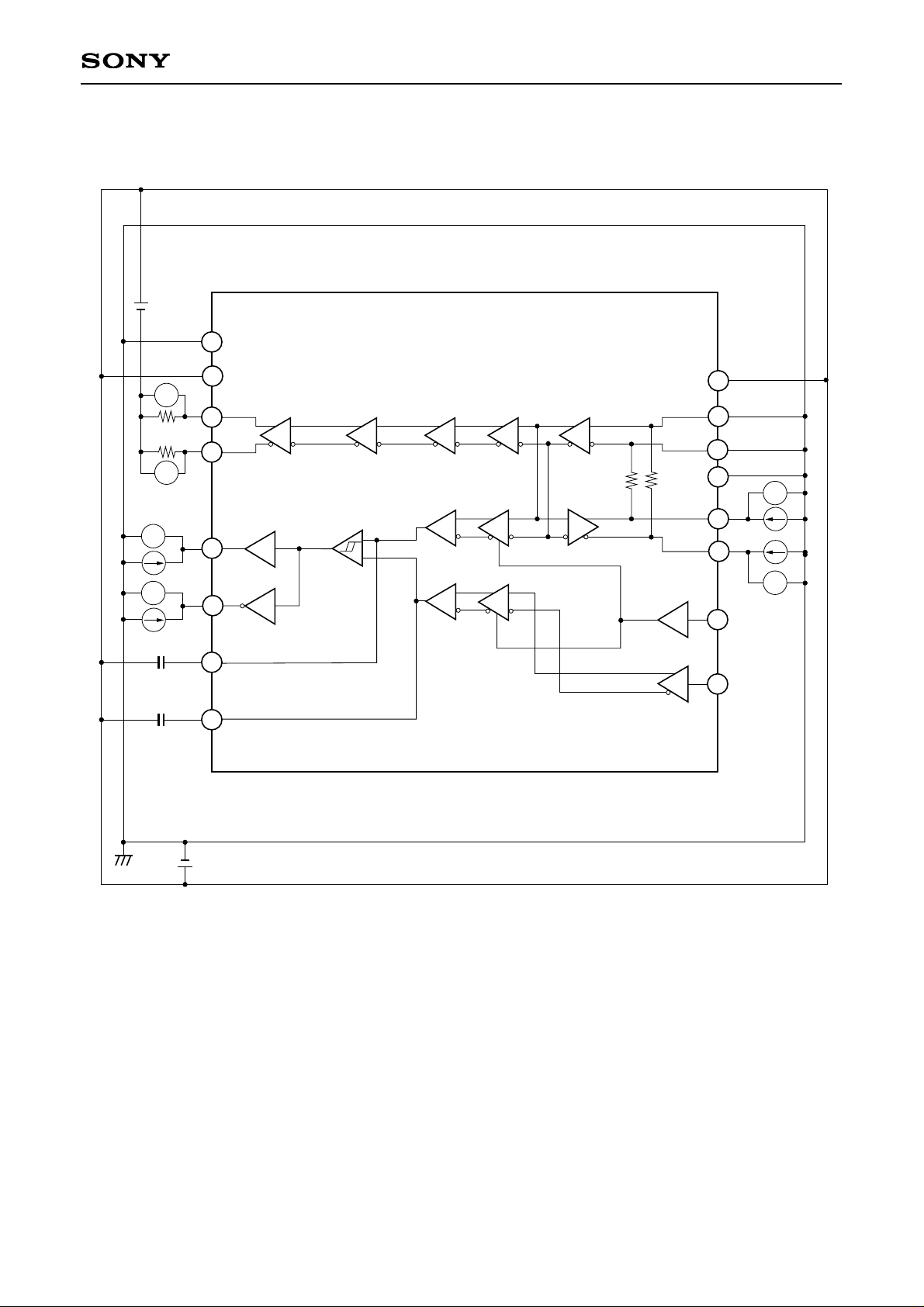
DC Electrical Characteristics Measurement Circuit
V
V
51Ω
2V
51Ω
3.14 to 5.25V
V
V
470pF
470pF
V
V
1
2
3
4
5
6
7
8
9
10
11
12
13
14
15
16
 Loading...