

Sony CXB1596AR Datasheet
10-bit Transceiver
Description
The CXB1596AR is a transceiver IC with a built-in
PLL for Fibre Channel and Gigabit Ethernet. For a
receiver 1.0625/1.25Gbaud serial data is received
and output as 10-bit parallel data; for a transmitter
10-bit parallel data is received and output as
1.0625/1.25Gbaud serial data.
Features
• Transmitter and receiver in a single chip
• ANSI X3T11 Fibre Channel compatible (FC_0) at
1.0625Gbaud
• IEEE802.3z Gigabit Ethernet compatible at
1.25Gbaud
• Conforms to 10-bit interface specification
• TTL/ECL compatible
• PLL for clock generation and clock & data recovery
• Byte synchronization detector (positive character of
Comma)
• Frequency autolock function
• Low power consumption (620mW typ.)
• 64-pin plastic LQFP package (10mm × 10mm)
Applications
• 1.0625Gbaud Fibre Channel Interface
• 1.25Gbaud Gigabit Ethernet Interface
• Work Station/Server/HDD Interface
• High-speed data communications
• Switched networks
Structure
Bipolar silicon monolithic IC
Absolute Maximum Ratings
• Supply voltage VCC –0.3 to +4 V
• TTL DC input voltage VI_T –0.5 to +5.5 V
• ECL DC input voltage VI_E VCC – 2 to VCC V
• ECL differential input voltage amplitude
VIS_E –4 to +4 V
• TTL high level output current
IOH_T –20 to 0 mA
• TTL low level output current
IOL_T 0 to 20 mA
• ECL output current IO_E –30 to 0 mA
• Storage temperature Tstg –65 to +150 °C
• Allowable power dissipation
PD 880 mW
Recommended Operating Conditions
• Supply voltage VCC 3.135 to 3.465 V
(3.3V Typ.)
• PECL AC coupling differential output load resistance
RL (to VCC –2V) 50 Ω
(to VEE) 150 Ω
• Ambient temperature Ta 0 to +70 °C
– 1 –
E99212-PS
Sony reserves the right to change products and specifications without prior notice. This information does not convey any license by
any implication or otherwise under any patents or other right. Application circuits shown, if any, are typical examples illustrating the
operation of the devices. Sony cannot assume responsibility for any problems arising out of the use of these circuits.
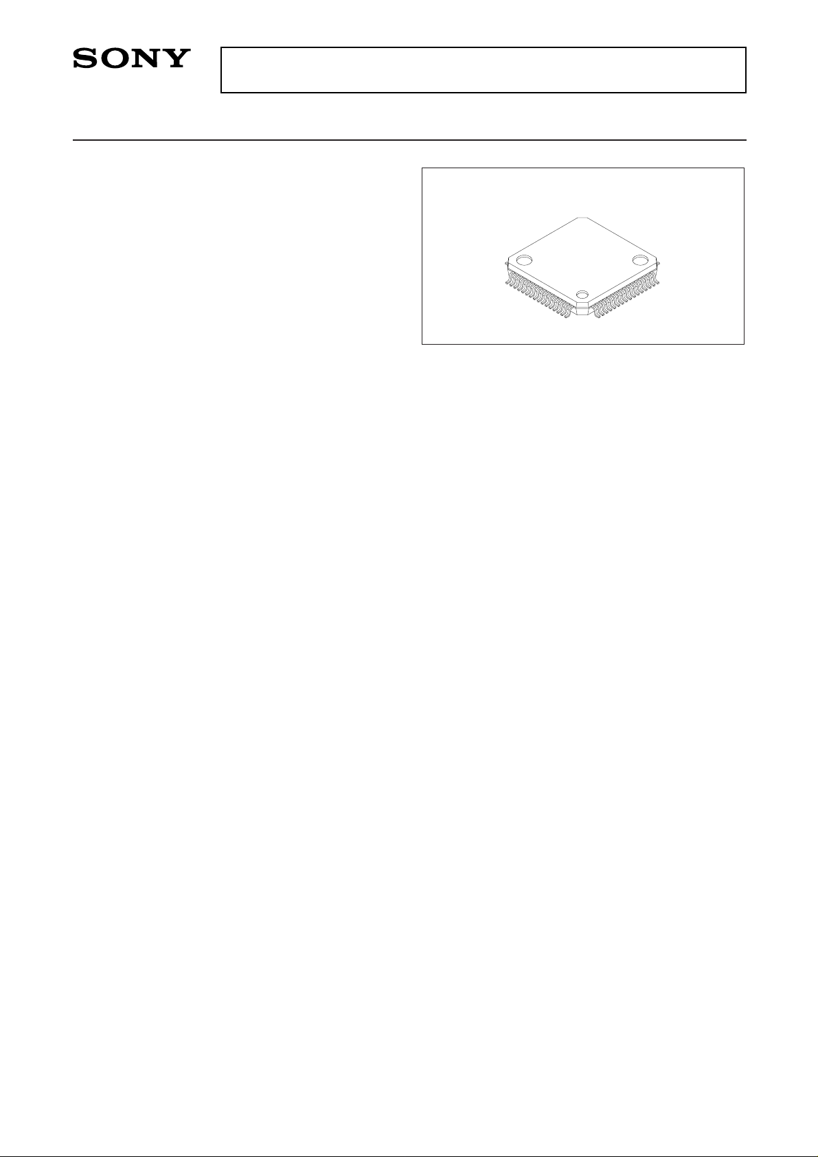
CXB1596AR
64 pin LQFP (Plastic)

– 2 –
CXB1596AR
Block Diagram
BYTSYNC
RBC1
RBC0
RX0 to 9
SDOUT
∗
SDOUT
SDIN
∗
SDIN
LBEN
BYTSYNCEN
LCKREF
∗
TX0 to 9
REFCLK
LPF_TX0
LPF_TX1
106.25MHz
(125MHz)
LCLK
106.25MHz
(125MHz)
TCLK
1.0625GHz
(1.25GHz)
RCLK
1.0625GHz
(1.25GHz)
FCLK
106.25MHz
(125MHz)
RDATA
Transmitter block
Receiver block
Frequencies in parentheses are for Gigabit Ethernet,
other frequencies are for Fibre Channel.
TXPLL
RXPLL
DIV
(1/10)
RBC
(1/2)
Parallel to
Serial
CONV.
Serial to
Parallel
CONV.
and
BYTE SYNC
I
O
10
10
10
D
Q
LPF_RX0
LPF_RX1
Pin Configuration (Top View)
49
50
51
52
53
54
55
56
57
58
59
60
61
62
63
64
LPF_RX1
V
CCP_RX
V
EEP_RX
SDIN
∗
V
CCE
SDIN
V
CCG
V
EEG
V
CCG
V
EEG
V
CCG
V
CCE
SDOUT
∗
SDOUT
V
CCE
V
EEE
1 2 3 4 5 6 7 8 9 10 11 12 13 14 15 16
VEET
TX0
TX1
TX2
RDSELN
TX3
TX4
TX5
TX6
V
CCG
TX7
TX8
TX9
V
EET
V
EEP_TX
LPF_TX0
33343536373839404142434445464748
LPF_RX0
BYTSYNC
V
EET
RX0
RX1
RX2
V
CCT
RX3
RX4
RX5
RX6
V
CCT
RX7
RX8
RX9
V
EET
17
18
19
20
21
22
23
24
25
26
27
28
29
30
31
32
V
EET
RBC0
RBC1
V
CCT
V
CCG
LCKREF
∗
TEST
∗
V
EEG
BYTSYNCEN
V
CCG
REFCLK
V
EEG
V
CCG
LBEN
V
CCP_TX
LPF_TX1
– 3 –
CXB1596AR
Pin Description
Pin
No.
1, 14,
32, 33,
46
2 to 4,
6 to 9,
11 to 13
5
10, 20,
23, 28,
55, 57,
59
15
16
17
18
19
VEET 0V
Negative power supply
for TTL output.
Power
supply
TX0 to TX9
TTL
level
Parallel data inputs.
Input data is converted to
serial data in order from
TX0.
TTL
input
RDSELN
TTL
High
level
Test input.
Set to TTL high level or
leave open.
Test
input
VCCG 3.3V
Positive power supply for
internal circuits.
Power
supply
VEEP_TX
0V
Negative power supply
for TXPLL.
Power
supply
LPF_TX0
LPF_TX1
—
External loop filter
connection for TX.
External
part
connection
pin
Symbol Type
Typical pin
voltage
Equivalent circuit
Description
VCCP_TX
3.3V
Positive power supply for
TXPLL.
Power
supply
LBEN
TTL
level
Loop back enable.
When high, the TX serial
output is serially input to
the RX side inside the IC.
When low, both transmit
and receive are enabled.
TTL
input
VEEG
VCCG
VEET
TTL_IN
LPF0
V
CCP
LPF1
V
EEP
VEEG
VCCG
VEET
TTL_IN
– 4 –
CXB1596AR
21, 25,
56, 58
22
24
26
27
29, 37,
42
VEEG 0V
Negative power supply
for internal circuits.
Power
supply
REFCLK
TTL
level
External reference clock
input.
TTL
input
BYTSYNCEN
TTL
level
Byte synchronization
enable.
When high, the Comma
detection circuit is
enabled to perform byte
synchronization.
TTL
input
TEST
∗
TTL
High
level
Test input.
Set to TTL high level or
leave open.
Test
input
LCKREF
∗
TTL
level
Forced reference clock
lock.
When low, the PLL is
forcibly locked to the
external reference clock
(REFCLK).
Normally set to high:
autolock mode.
TTL
input
VCCT 3.3V
Positive power supply for
TTL output.
Power
supply
VEEG
VCCG
VEET
TTL_IN
VEEG
VCCG
VEET
TTL_IN
VEEG
VCCG
VEET
TTL_IN
VEEG
VCCG
VEET
TTL_IN
Pin
No.
Symbol Type
Typical pin
voltage
Equivalent circuit
Description
– 5 –
CXB1596AR
30
31
34 to 36,
38 to 41,
43 to 45
47
48
49
50
51
RBC1
RBC0
TTL
level
Receive side byte clocks
recovered from the serial
data.
RBC1 and RBC0 output
clocks which are 180
degrees out of phase.
TTL
output
RX0 to
RX9
TTL
level
Parallel data outputs.
Serial data is converted
to parallel data in order
starting from RX0 and
ending with RX9.
TTL
output
BYTSYNC
TTL
level
Byte synchronization
detection signal.
This pin outputs high for
a 1 byte period when the
Comma signal is
detected.
TTL
output
LPF_RX0
LPF_RX1
—
External loop filter
connection for RX.
External
part
connection
pin
VCCP_RX 3.3V
Positive power supply for
RXPLL.
Power
supply
VEEP_RX 0V
Negative power supply
for RXPLL.
Power
supply
VCCT
VEET
TTL_OUT
LPF0
V
CCP
LPF1
V
EEP
VCCT
VEET
TTL_OUT
VCCT
VEET
TTL_OUT
Pin
No.
Symbol Type
Typical pin
voltage
Equivalent circuit
Description
 Loading...