

Sony CXB1595AN Datasheet
CXB1595AN
Fibre Channel Repeater
Description
The CXB1595AN is a clock and data recovery IC
for fibre channel 1.0625Gbaud with a built-in PLL.
This IC incorporates a port bypass circuit and is
suitable for disk array and FC-AL HUB, etc.
Features
• Conforms to ANSI X3T11 Fibre Channel standard
• Single 3.3V power supply
• Low power consumption: 380mW (Typ.)
• Low jitter
• PLL lock detection circuit
• Port bypass circuit
• Small plastic package (30-pin SSOP)
Applications
• Fibre channel arbitrated loop 1.0625Gbaud HUB
• Disk array
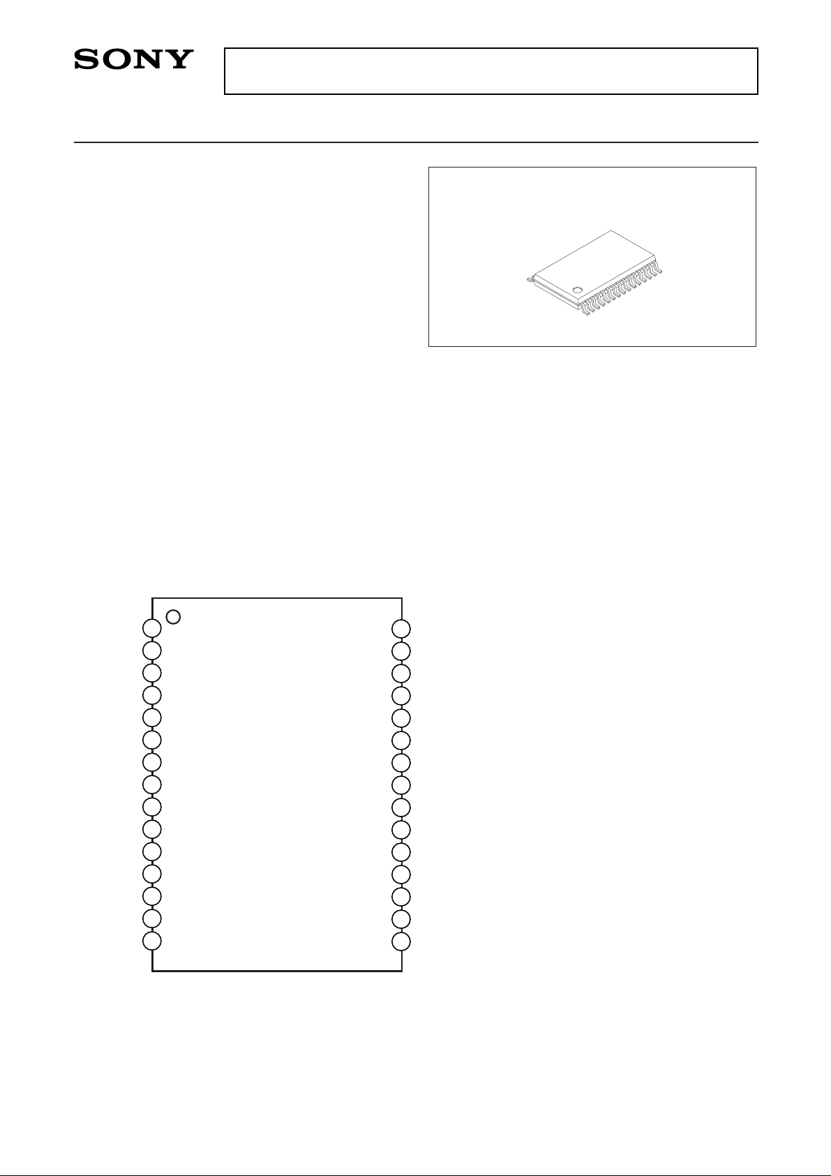
Pin Configuration
Structure
Bipolar silicon monolithic IC
– 1 –
E99632-PS
Sony reserves the right to change products and specifications without prior notice. This information does not convey any license by
any implication or otherwise under any patents or other right. Application circuits shown, if any, are typical examples illustrating the
operation of the devices. Sony cannot assume responsibility for any problems arising out of the use of these circuits.
30 pin SSOP (Plastic)
1
2
3
4
5
6
7
8
9
10
11
12
13
14
15
REFCLK
LKDT
V
EET
DIAG_OUT
DIAG_OUTN
VCCE
LOOP_IN
LOOP_INN
VEEG
PORT_IN
PORT_INN
LKREFN
VEEP
LPF1
LPF2
16
17
18
19
20
21
22
23
24
25
26
27
28
29
30
CDR_SELN
DIAG_SELN
LOOP_SELN
DIAG_IN
DIAG_INN
V
CCG
LOOP_OUT
LOOP_OUTN
VCCE
PORT_OUT
PORT_OUTN
VEEE
PORT_SEL0N
PORT_SEL1N
VCCP
– 2 –
CXB1595AN
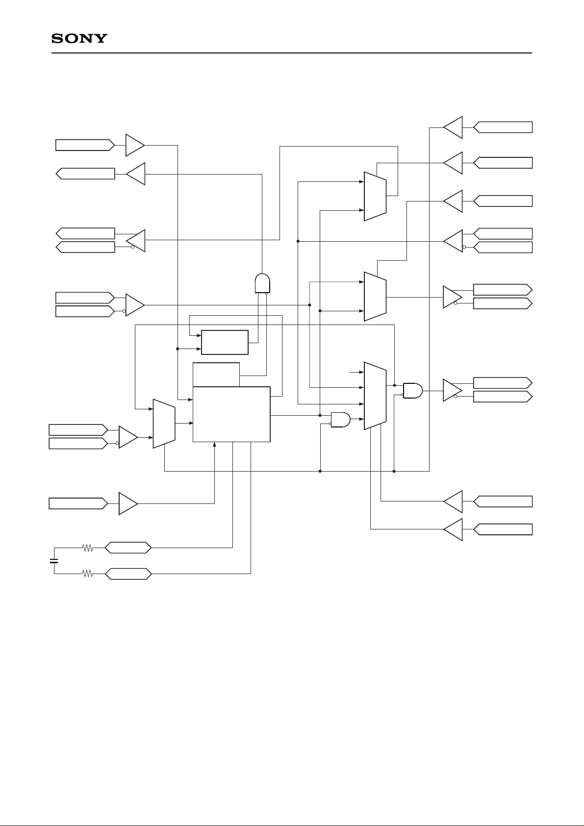
Block Diagram
Y
0
1
S
Y
0
1
S
Y
1
0
S
Y
11
00
01
10
S1 S0
LOOP_OUTN
(ECL/O)
LOOP_OUT
DIAG_INN
(ECL/I)
CDR_SELN
(TTL/I)
DIAG_SELN
(TTL/I)
LOOP_SELN
(TTL/I)
PORT_SEL0N
(TTL/I)
PORT_SEL1N
(TTL/I)
DIAG_IN
PORT_OUTN
(ECL/O)
PORT_OUT
DIAG_OUT
DIAG_OUTN
(ECL/O)
LOOP_IN
LOOP_INN
(ECL/I)
LKREFN
(TTL/I)
LPF1
LPF2
REFCLK
(TTL/I)
53.125MHz
1.0625Gboud
1.0625Gboud
Recovered clock
Retimed data
Low
LKDT
(TTL/O)
PORT_IN
PORT_INN
(ECL/I) 1.0625Gboud
Frequency
Detector
Unlock
Detector
Clock and Data
Recovery
– 3 –
CXB1595AN
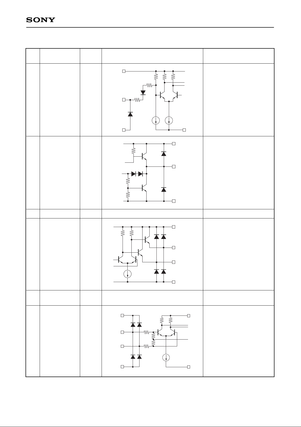
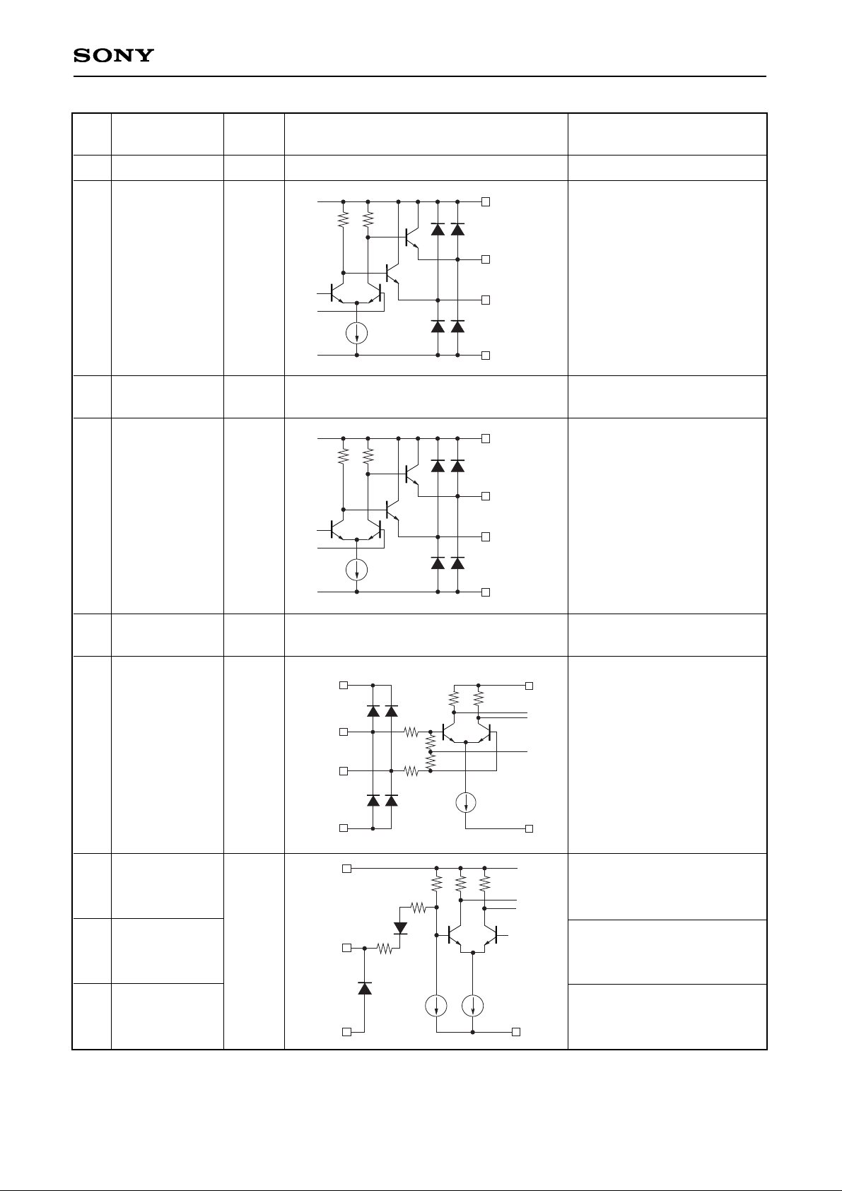
Pin Description
Pin
No.
Symbol Type Equivalent circuit Description
REFCLK
Input
TTL
1
Reference clock.
This pin is used for the PLL
to take the frequency. Input
53.125MHz to this pin.
VCCG
V
EET VEEG
TTL_IN
LKDT
VEET
Output
TTL
Ground
2
3
PLL lock detection signal
output.
Outputs high level when PLL
is locked to the serial data.
Outputs low level when
LKREFN is in the low level or
the serial data isn't locked to
the serial input data.
Ground for TTL I/O: 0V.
VCCE
Power
supply
6
Power supply for ECL l/O:
3.3V ± 5%.
VEET
VCCE
TTL_OUT
DIAG_OUT
DIAG_OUTN
Output
ECL
4
5
Differential serial data output.
VCCE
ECL_OUT
ECL_OUTN
VEEE
LOOP_IN
LOOP_INN
Input
ECL
7
8
Differential serial data input.
VCCE
ECL_IN
ECL_INN
VEEE
VCCG
VEEG
V
CCE – 1.3V
– 4 –
CXB1595AN
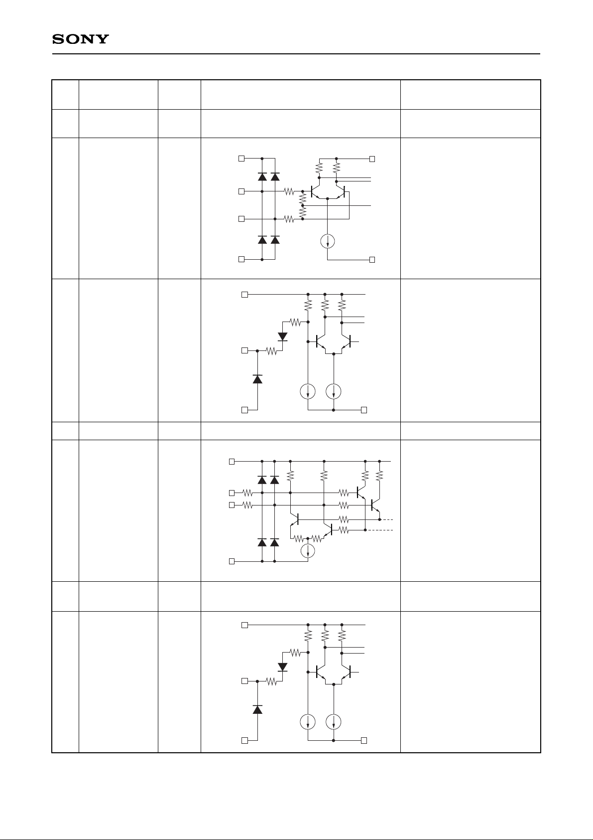
Pin
No.
Symbol Type Equivalent circuit Description
LKREFN
Input
TTL
12
Lock to reference.
An active low input.
LKREFN causes the PLL lock
to the REFCLK.
VCCG
V
EET VEEG
TTL_IN
LPF1
LPF2
External
circuit
node
14
15
Connect to external loop filter.
VCCP
LPF1
LPF2
VEEP
VEEG
Ground
9
Ground for internal logic Gate:
0V.
VEEP
Ground
13
Ground for PLL: 0V.
VCCP
Power
supply
16
Power supply for PLL:
3.3V ± 5%.
PORT_IN
PORT_INN
Input
ECL
10
11
Differential serial data input.
VCCE
ECL_IN
ECL_INN
VEEE
VCCG
VEEG
V
CCE – 1.3V
PORT_SEL1N
PORT_SEL0N
Input
TTL
17
18
Selection for PORT_OUT.
VCCG
V
EET VEEG
TTL_IN
– 5 –
CXB1595AN
Pin
No.
Symbol Type Equivalent circuit Description
VEEE
Ground
19
Ground for ECL I/O: 0V.
VCCE
Power
supply
22
Power supply for ECL I/O:
3.3V ± 5%.
VCCG
Power
supply
25
Power supply for internal logic
gate: 3.3V ± 5%.
PORT_OUTN
PORT_OUT
Output
ECL
20
21
Differential serial data output.
VCCE
ECL_OUT
ECL_OUTN
VEEE
LOOP_OUTN
LOOP_OUT
Output
ECL
23
24
Differential serial data output.
VCCE
ECL_OUT
ECL_OUTN
VEEE
DIAG_INN
DIAG_IN
Input
ECL
Input
TTL
26
27
Differential serial data input.
VCCE
ECL_IN
ECL_INN
VEEE
VCCG
VEEG
V
CCE – 1.3V
VCCG
V
EET VEEG
TTL_IN
LOOP_SELN
DIAG_SELN
28
29
CDR_SELN
30
Selection for LOOP_OUT.
See table 9.
Selection for DIAG_OUT.
See table 9.
Selection for CDR input.
See table 9.
 Loading...