

Sony CXB1581Q Datasheet
21
22
23
24
25
26
27
28
29
30
40
39
38
37
36
35
34
31
32
33
41
42
43
44
45
46
47
48
49
50
51
52
53
54
55
56
57
58
59
60
70
69
68
67
63
64
65
66
61
62
71
72
73
74
75
76
77
78
79
80
2
3
4
5
6
7
8
9
10
11
12
13
14
15
16
17
18
19
20
1
VEEE
V
EEE
EXCLK
∗
EXCLK
SDIN
∗
SDIN
V
CCE
V
CCE
SDOUT
∗
SDOUT
VCCE
LBOUT
∗
LBOUT
VCCE
V
CCE
PSOUT
∗
PSOUT
V
EEE
TJMON1
TJMON2
NC
ALTSEL
∗
TPGEN
PPSEL
SDRSEL
BYTSEL
TBC_IN
V
CCG
V
EEG
TX19
V
EEG
TX18
TX17
TX16
TX15
TX14
TX13
TX12
TX11
TX10
LPF_A
LPF_B
V
EE
P2
REXT
V
CC
P
CLR
∗
NC
LDALM
R_FLT
SDDIS
LBEN
SDSEL
TCLKSEL
∗
V
EE
P1
V
EE
P1
V
CC
G
V
EE
G
V
CC
P
V
CC
G
ECLKSEL
∗
V
CC
G
FAULT
V
CC
T3
LKDT
∗
V
EE
T
V
EE
T
TBC_OUT
TX00
V
EE
G
V
CC
T5
V
CC
G
TX01
TX02
TX03
TX04
TX05
TX06
TX07
TX08
TX09
Description
The CXB1581Q is a transmitter IC with a built-in
PLL for high-speed serial data transmission. It can
be used together with the receiver IC CXB1582Q as
a chip set, and 1062.5Mbaud, 20-bit or 531.25Mbaud,
10-bit operation can be selected.
Features
• Conforms to ANSI X3T11 Fibre channel standard
• Supports GLM (Gigabaud Link Module) interface
• Built-in PLL for synthesizing a low-jitter clock
• Single 3.3V power supply or dual 3.3V/5V power
supply (for 5V TTL interface) operation can be
selected.
• Low power consumption: 830mW (Typ.) when
operating with a single 3.3V power supply
• 1062.5Mbaud, 20-bit or 531.25Mbaud, 10-bit
operation can be selected.
• Test pattern (±K28.5) generation circuit
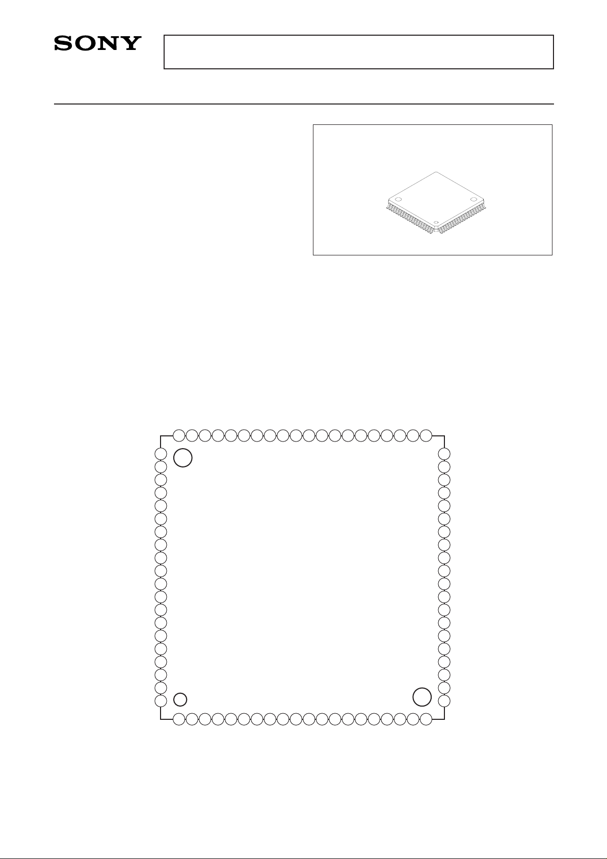
Pin Configuration
Applications
Fibre channel 1062.5Mbaud and 531.25Mbaud
communications
Structure
Bipolar silicon monolithic IC
– 1 –
CXB1581Q
E95912A64-ST
Fibre Channel Transmitter
Sony reserves the right to change products and specifications without prior notice. This information does not convey any license by
any implication or otherwise under any patents or other right. Application circuits shown, if any, are typical examples illustrating the
operation of the devices. Sony cannot assume responsibility for any problems arising out of the use of these circuits.
80 pin QFP (Plastic)
– 2 –
CXB1581Q
Absolute Maximum Ratings (VEEE, VEET, VEEG, VEEP = 0V)
Item Unit
V
V
V
V
V
mA
mA
mA
°C
°C
4
VCCG + 5,
or 5.5
5.5
VCC
2
0
20
0
70
150
–0.3
VCCG – 2,
or –0.3
–0.5
VCC – 2
–2
–20
0
–30
–55
–65
VCC
VCCT5
VI_T
VI_E
VIS_E
IOH_T
IOL_T
IO_E
Ta
Tstg
Supply voltage (excluding VCCT5)
Supply voltage for TTL output
TTL DC input voltage
ECL DC input voltage
ECL differential input voltage
TTL output current (High level)
TTL output current (Low level)
ECL output current
Operating ambient temperature
Storage temperature
Max.Typ.Min.Symbol
Recommended Operating Conditions (VEEE, VEET, VEEG, VEEP = 0V)
During single 3.3V power supply operation
Item Unit
V
°C
3.465
70
3.33.135
0
VCC
Ta
Supply voltage (including VCCT5)
Ambient temperature
Max.Typ.Min.Symbol
During dual 3.3V/5V power supply operation (VCCT3 open)
Item Unit
V
V
°C
3.465
5.25
70
3.3
5
3.135
4.75
0
VCC
VCCT5
Ta
Supply voltage (excluding VCCT5)
Power supply for TTL output
Ambient temperature
Max.Typ.Min.Symbol
– 3 –
CXB1581Q
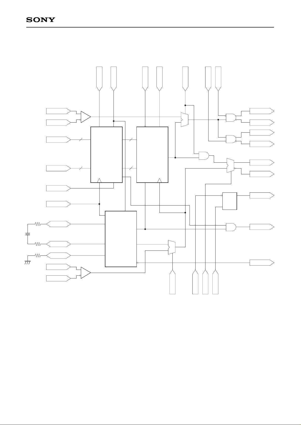
Block Diagram
1
0
1
0
R
RSFF
S
Q
LKDT
∗
TBC OUT
FAULT
PSOUT
∗
LBOUT
∗
SDOUT
∗
PSOUT
LBOUT
SDOUT
ECLKSEL
∗
R_FLT
TCLKSEL
∗
LDALM
SDIN
SDIN
∗
TX00 to 09
TX10 to 19
PPSEL
TBC_IN
LPF_A
LPF_B
REXT
EXCLK
EXCLK
∗
ALTSEL
∗
TPGEN
SDSEL
LBEN
SDDIS
SDRSEL
BYTSEL
1
0
10
10
10
10
53.125MHz
53.125Mbaud
53.125Mbaud
531.25
or 1062.5Mbaud
TBC_EN
53.125MHz
531.25 or
1062.5MHz
Parallel Data
Input Buffer
P/S Converter
PLL
– 4 –
CXB1581Q
Pin Description
Pin
No.
Symbol Type
Typical pin
I/O voltage
Equivalent circuit Description
1, 21,
32, 49
VEEG
Power
supply
0V
Negative power
supplies for internal
logic gate.
2, 20,
33,50,51VCCG
Power
supply
3.3V
Positive power
supplies for internal
logic gate.
3, 4
VEET
Power
supply
0V
Negative power
supplies for TTL
output.
5
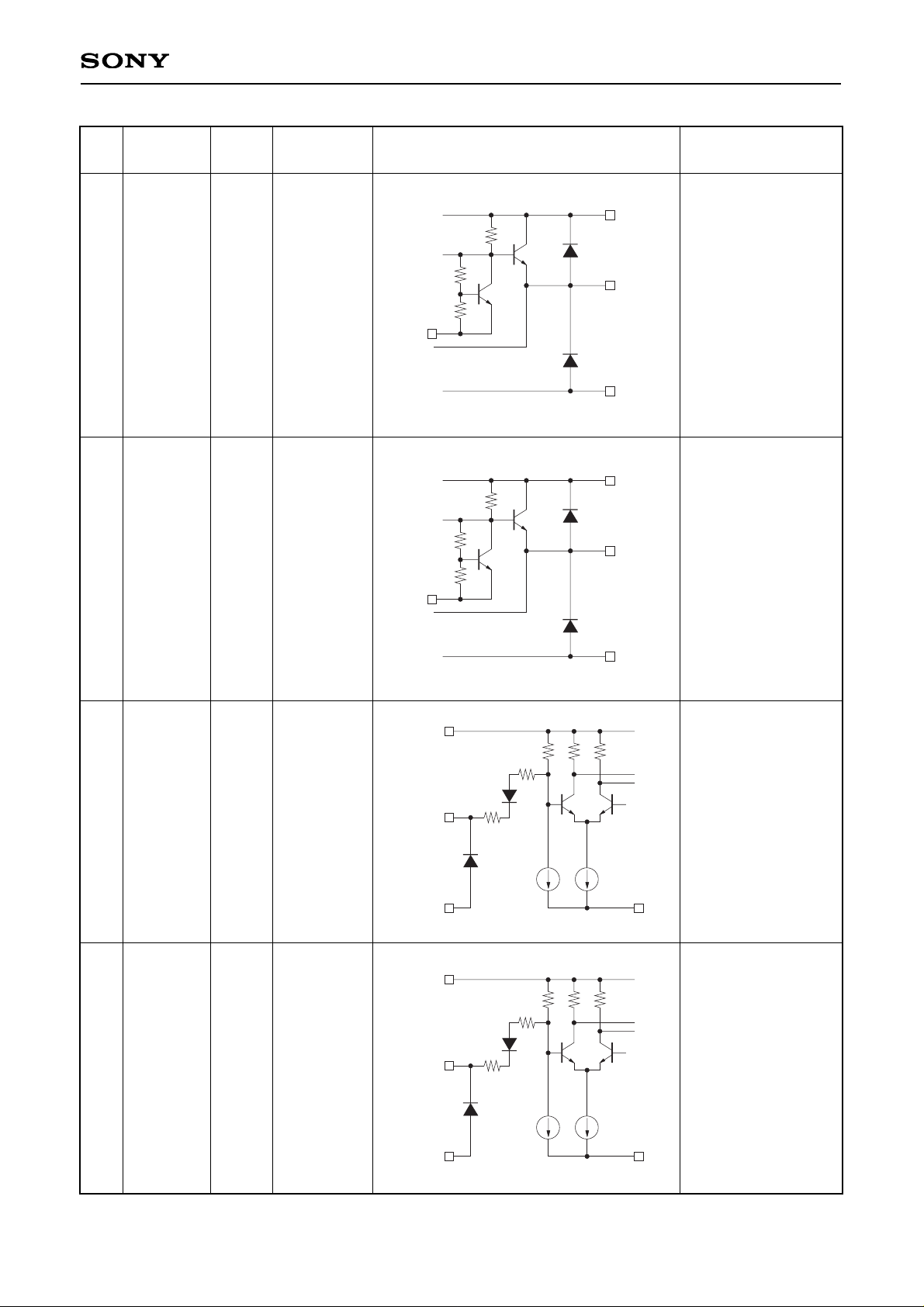
LKDT
∗
TTL
output
TTL level
PLL lock detection
signal output. This
pin outputs low level
when the PLL is
locked to TBC_IN
and operating
normally, and high
level when the PLL
is not operating
normally.
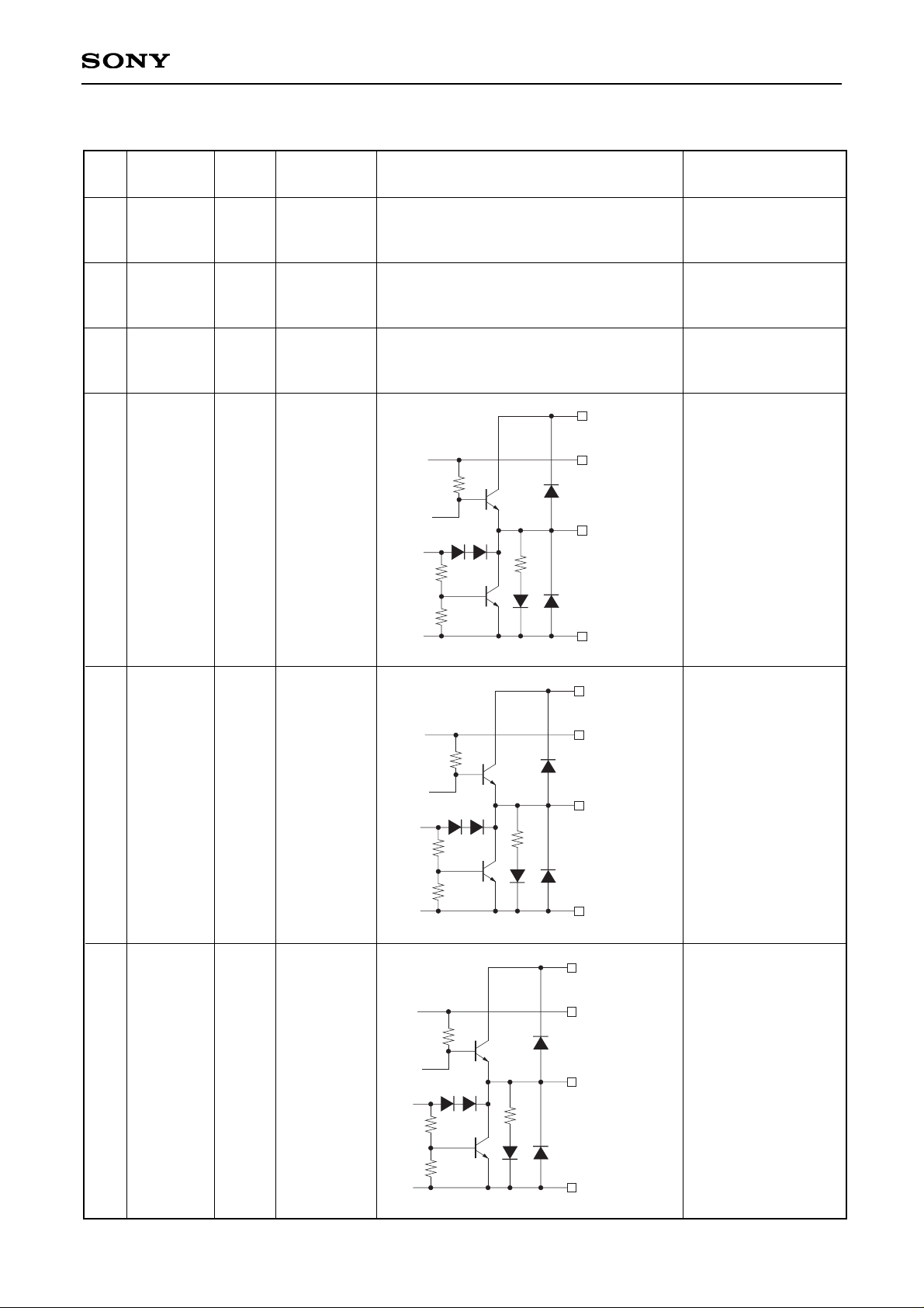
VEET
VCCT5
VCCT3
LKDT
∗
6
FAULT
TTL
output
TTL level
FAULT signal output.
This pin is used for
the FAULT signal in
the GLM standard.
This pin outputs high
level at the rising
edge of LDALM and
low level at the falling
edge of R_RLT. (See
Table 3.)
VEET
VCCT5
VCCT3
FAULT
7
TBC_OUT
TTL
output
TTL level
Transmission byte
clock output
(53.125MHz).
This clock is
generated by
frequency-dividing
the transmission bit
clock (1.0625GHz or
531.25MHz).
VEET
VCCT5
VCCT3
TBC_OUT
—
—
—
– 5 –
CXB1581Q
Symbol Type Equivalent circuit Description
8
VCCT3
Power
supply
3.3V or open
Positive power
supply for TTL
output. Set to 3.3V
when using the IC
with a single 3.3V
power supply; leave
open when using
the IC with a dual
3.3V/5V power
supply.
VCCT5
VEET
VCCT3
VCCG
9
VCCT5
Power
supply
3.3V or 5V
Positive power
supply for TTL
output. Set to 3.3V
when using the IC
with a single 3.3V
power supply; to 5V
when using the IC
with a dual 3.3V/5V
power supply.
VCCT5
VEET
VCCT3
VCCG
10
to
19
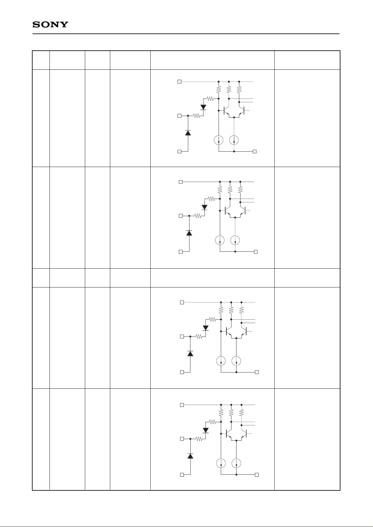
TX00 to 09
TTL
input
TTL level
Parallel data inputs
(Byte_0).
VEET
VCCG
TX00 to 09
V
EET
22
to
31
TX10 to 19
TTL
input
TTL level
Parallel data inputs
(Byte_1).
VEET
VCCG
TX10 to 19
V
EET
Pin
No.
Typical pin
I/O voltage
– 6 –
CXB1581Q
34
TBC_IN
TTL
input
TTL level
Transmission byte
clock input
(53.125MHz).
VEET
VCCG
TBC_IN
V
EET
35
BYTSEL
TTL
input
TTL level
Byte selection.
(See Table 2.)
VEET
VCCG
BYTSEL
V
EET
36
SDRSEL
TTL
input
TTL level
Serial data
transmission rate
selection. Setting
this pin to low level
selects 531.25Mbaud
mode and to high
level selects
1.0625Gbaud mode.
VEET
VCCG
SDRSEL
V
EET
37
PPSEL
TTL
input
TTL level
Ping-Pong mode
selection. (See
Table 2 and the
Timing Charts.)
VEET
VCCG
PPSEL
V
EET
Symbol Type Equivalent circuit Description
Pin
No.
Typical pin
I/O voltage
– 7 –
CXB1581Q
38
TPGEN
TTL
input
TTL level
Test pattern
generation control.
Inputting high level
to this pin generates
positive or alternating
disparity K28.5 (one
of the 8B10B
conversion codes) as
the serial transfer
data.
VEET
VCCG
TPGEN
V
EET
39
ALTSEL
∗
TTL
input
TTL level
Alternating disparity
selection. The test
pattern generated
when TPGEN is set
to high level
becomes alternating
disparity K28.5 if this
pin is set to low level,
and positive disparity
K28.5 if this pin is set
to high level.
40,
41
NC
Open
No connection.
VEET
VCCG
ALTSEL
∗
V
EET
42
ECLKSEL
∗
TTL
input
TTL high
level or 3.3V
External clock
selection. When this
pin is set to low level,
the clock input to
EXCLK is used as
the transmission bit
clock.
VEET
VCCG
ECLKSEL
∗
V
EET
43
TCLKSEL
∗
TTL
input
TTL high
level or 3.3V
Transmission bit
clock output
selection. When this
pin is set to low level,
the transmission bit
clock is output from
PSOUT. (See Table
1.)
VEET
VCCG
TCLKSEL
∗
V
EET
Symbol Type Equivalent circuit Description
Pin
No.
Typical pin
I/O voltage
 Loading...