

Sony CXB1577Q Datasheet

– 1 –
CXB1577Q
E96Z24-PS
Post-Amplifier for Optical Fiber Communication Receiver
Description
The CXB1577Q achieves the 2R optical-fiber
communication receiver functions (Reshaping and
Regenerating) on a single chip. This IC is equipped
with the signal detection function, which is used to
enable TTL/ECL outputs. Also, the output disable
function performs the output shutdown. 3.3V/5.0V
can be used for the supply voltage.
Features
• Output disable function (TTL input)
• Signal detection function (TTL/ECL output)
• Supply voltage supports both 3.3V/5.0V
Applications
• SONET/SDH: 622.08Mbps
• Fibre Channel: 531.25Mbps
: 1.062Gbps
• Gigabit-Ethernet: 1.25Gbps
Absolute maximum Ratings
• Supply voltage VCC – VEE –0.3 to +7 V
• Storage temperature Tstg –65 to +150 °C
• Input voltage difference VD – VD Vdif 0 to +2 V
• SW input voltage Vi VEE to VCC V
• ECL output current IOQ/SD-ECL –30 to 0 mA
• TTL output current (High level) IOH SD-TTL –20 to 0 mA
• TTL output current (Low level) IOL SD-TTL 0 to 20 mA
Recommended Operating Conditions
• Supply voltage VCC – VEE 3.3 ± 0.2/5 ±0.25 V
• Termination voltage (for data) VCC – VTD 1.8 to 2.2 V
• Termination voltage (for alarm 1,alarm 2) VTA VEE V
• Termination resistance (for data) RTD 46 to 56 Ω
• Termination resistance (for alarm 1) RTA1 240 to 300 Ω
• Termination resistance (for alarm 2) RTA2 460 to 560 Ω
• Operating temperature Ta –40 to +85 °C
Structure
Bipolar silicon monolithic IC
Sony reserves the right to change products and specifications without prior notice. This information does not convey any license by
any implication or otherwise under any patents or other right. Application circuits shown, if any, are typical examples illustrating the
operation of the devices. Sony cannot assume responsibility for any problems arising out of the use of these circuits.
40 pin QFP (Plastic)
—
—

– 2 –
CXB1577Q
Block Diagram and Pin Configuration
V
EE
4
2
3
4
5
6
7
8
9
10
11
12
13
14
15
16
17
18
19
20
21
22
23
24
25
2627
28
29
30
40
39
38
37
36
35
34
31
32
33
1
N.C.
V
EE
3
ODIS
SW
VC2
N.C.
N.C.
V
EE
1
V
EE
2
N.C.
N.C.
VC3
CAP3
CAP2
V
EE
2
V
EE
I
DN
UP
N.C.
VCC3
QB
Q
VC1
SDB-ECL
SDB-TTL
SD-TTL
V
CC4
TM
V
CC1
N.C.
CAP1B
CAP1
D
V
CC2
V
CC
2
VC0
DB
V
EE1
SD-ECL
peak hold
peak hold
∆V
– 3 –
CXB1577Q
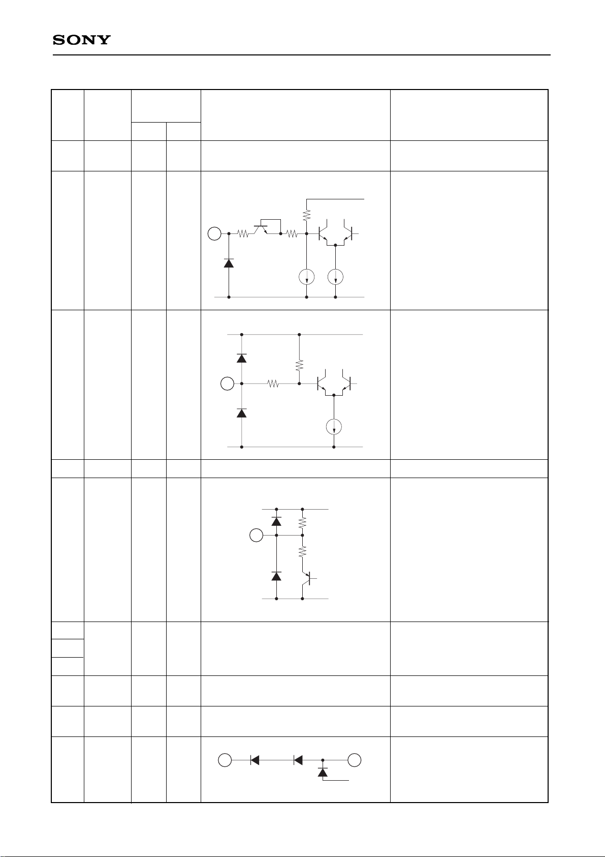
Pin Description
Pin
No.
1
VEE3
–3.3V
/
–5V
Negative power supply for ECL
output buffer.
Switches the identification
maximum voltage amplitude.
High voltage when open; the
identification maximum voltage
amplitude becomes 40mVp-p.
Low voltage when connected
to VEE; the amplitude becomes
20mVp-p.
2
ODIS
0V
(Open)
or
–3.3V
/
–5V
3
SW
0V
(Open)
or
–3.3V
/
–5V
Switches 3.3V/5V. Short this pin
to Vcc for 3.3V between Vcc and
VEE. Leave this pin open for 5V
between Vcc and VEE.
No connected.
Negative power supply for digital
block.
Negative power supply for analog
block.
Chip temperature monitor.
4
VCC2
0V
6
VC2
0V
/
–1.7V
(Open)
7
N.C.
8
9
10
5
VEE2
–3.3V
/
–5V
VEE1
–3.3V
/
–5V
11
TM
–1.8V
/ –3.5V
Controls the output shutdown
function. High voltage when
open; the Q output is fixed to
Low. Low voltage when
connected to VEE; the D input
results in the Q output with ECL
level. TTL level is also available.
Symbol
Typical pin
voltage
DC
AC
Equivalent circuit
Description
VCC2
VEE2
40k
60k
3
2
VCC2
VEE2
VREF
10k
10k
300
5
VCC2
VEE2
6k
2k
Positive power supply for digital block.
10
11
VEE1
– 4 –
CXB1577Q
12
13
14
15
16
17
18
19
20
21
22
23
24
25
VCC1
VC0
N.C.
CAP1B
CAP1
DB
D
VEE1
VCC2
N.C.
UP
DN
VEEI
VEE2
0V
–0.9V
to
–1.7V
–0.9V
to
–1.7V
Positive power supply for analog block.
No connected.
Switches 3.3V/5V. Short this pin
to Vcc for 3.3V between Vcc and
VEE. Leave this pin open for 5V
between Vcc and VEE.
Pins 15 and 16 connect a
capacitor which determines the
cut-off frequency for DC
feedback block.
Pins 17 and 18 are input pins
for limiting amplifier block. Input
the signal with AC coupled.
DC
AC
VCC3
VEE3
6k
2k
13
Negative power supply for analog
block.
Positive power supply for digital block.
No connected.
Connects a resistor for alarm
level setting.
Default voltage can be generated
without an external resistor by
shorting the VEEI pin to VEE.
Generates the default voltage
between UP and DOWN.
The voltage (8.0mV for input
conversion) can be generated
between UP and DOWN (Pins
22 and 23)
as alarm setting level
by connecting this pin to VEE.
–1.3V
–1.3V
–3.3V
/–5V
0V
–3.3V
/–5V
–3.3V
/–5V
16
15
1k
18
17
1k
V
CC1
V
EE1
2007.5k
100p
2007.5k
Pin
No.
Symbol
Typical pin
voltage
Equivalent circuit
Description
23
24
VCC2
VEE2
100
22
986
100
140.9
140.9
VCS
SW
SW
Negative power supply for digital
block.
0V
/
–1.7V
(Open)
– 5 –
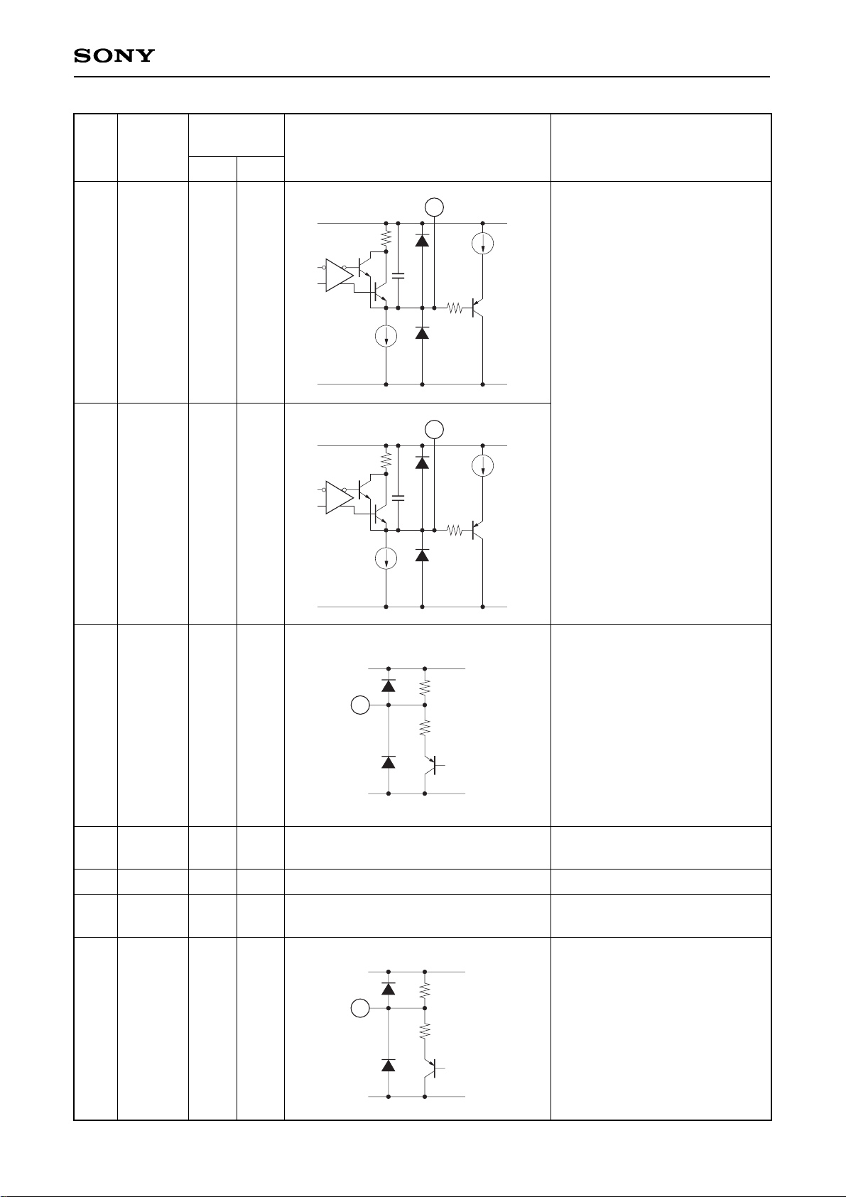
CXB1577Q
32
DC
AC
26
CAP2
–1.8V
Connects a peak hold circuit
capacitor for alarm block.
470pF should be connected
to Vcc each.
CAP2 pin connects a peak
hold capacitor for alarm
level setting block.
CAP3 pin connects a peak
hold capacitor for limiting
amplifier signal.
26
VCC2
VEE2
80
200
5µA
10p
27
CAP3
–1.8V
28
29
30
31
VC3
VEE4
N.C.
VCC4
0V
/–1.7V
(Open)
–3.3V
/–5V
0V
Switches 3.3V/5V. Short this pin
to Vcc for 3.3V between Vcc and
VEE. Leave this pin open for 5V
between Vcc and VEE.
VCC2
VEE2
80
200
5µA
10p
27
VCC3
VEE3
6k
2k
28
VC1
0V
–1.7V
(Open)
Switches 3.3V/5V. Short this pin
to Vcc for 3.3V between Vcc and
VEE. Leave this pin open for 5V
between Vcc and VEE.
VCC3
VEE3
6k
2k
32
Pin
No.
Symbol
Typical pin
voltage
Equivalent circuit
Description
Negative power supply for TTL
output buffer.
No connected.
Positive power supply for TTL
output buffer.

– 6 –
CXB1577Q
DC
AC
33
SD-TTL
VEE
or
VEE +
3V
Alarm signal TTL level output.
VCC4
VEE4
33
40k
34
SDB-TTL
VEE
or
VEE +
3V
3536SD-ECL
SDB-ECL
–0.9V
or
–1.7V
–0.9V
or
–1.7V
Alarm signal ECL level output.
Terminate this pin in 510Ω to V
EE
at
VEE = 5V; in 270Ω
to V
EE at VEE
= 3.3V.
VCC4
VEE4
40k
34
36
35
VCC3
VEE3
Pin
No.
Symbol
Typical pin
voltage
Equivalent circuit
Description
Alarm signal TTL level output.
– 7 –
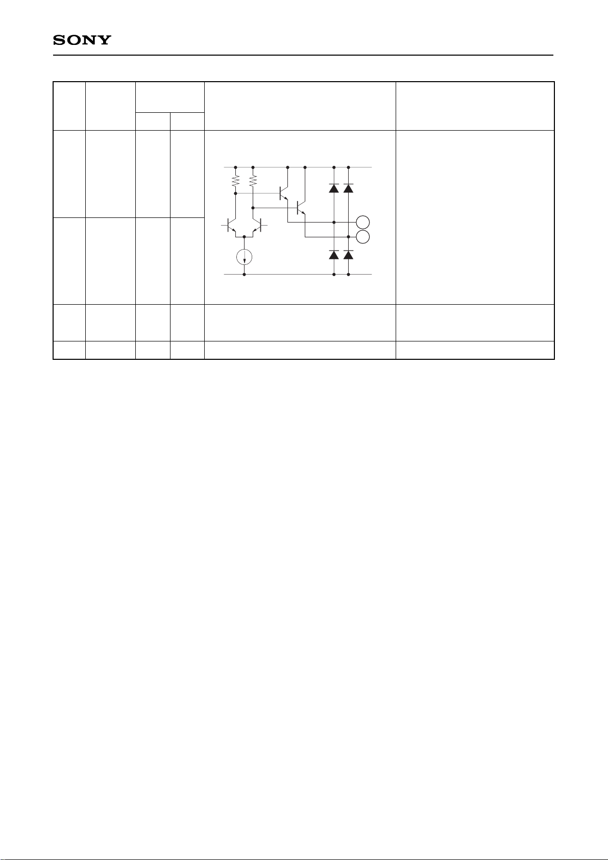
CXB1577Q
DC
AC
37
Q
–0.9V
or
–1.7V
Data signal output. Terminates
this pin in 50Ω to VTT =
Vcc–2V.
VCC3
VEE3
38
37
38 QB
–0.9V
or
–1.7V
39
40
VCC3
N.C.
0V
Pin
No.
Symbol
Typical pin
voltage
Equivalent circuit
Description
Positive power supply for ECL
output buffer.
No connected.
 Loading...