

Sony CXB1567Q Datasheet
CXB1567Q
For the availability of this product, please contact the sales office.
Limiting Amplifier for Optical Fiber Communication Receiver
Description
The CXB1567Q achieves the 2R optical-fiber
communication receiver functions (Reshaping and
Regenerating) on a single chip. This IC is also
equipped with the signal interruption alarm output
function, which is used to discriminate the existence
of data input.
Features
• Auto-offset canceller circuit
• Signal interruption alarm outputs
• Single 5V power supply
Applications
• SONET/SDH: 622.08Mb/s
• Fiber channel: 531.25Mb/s
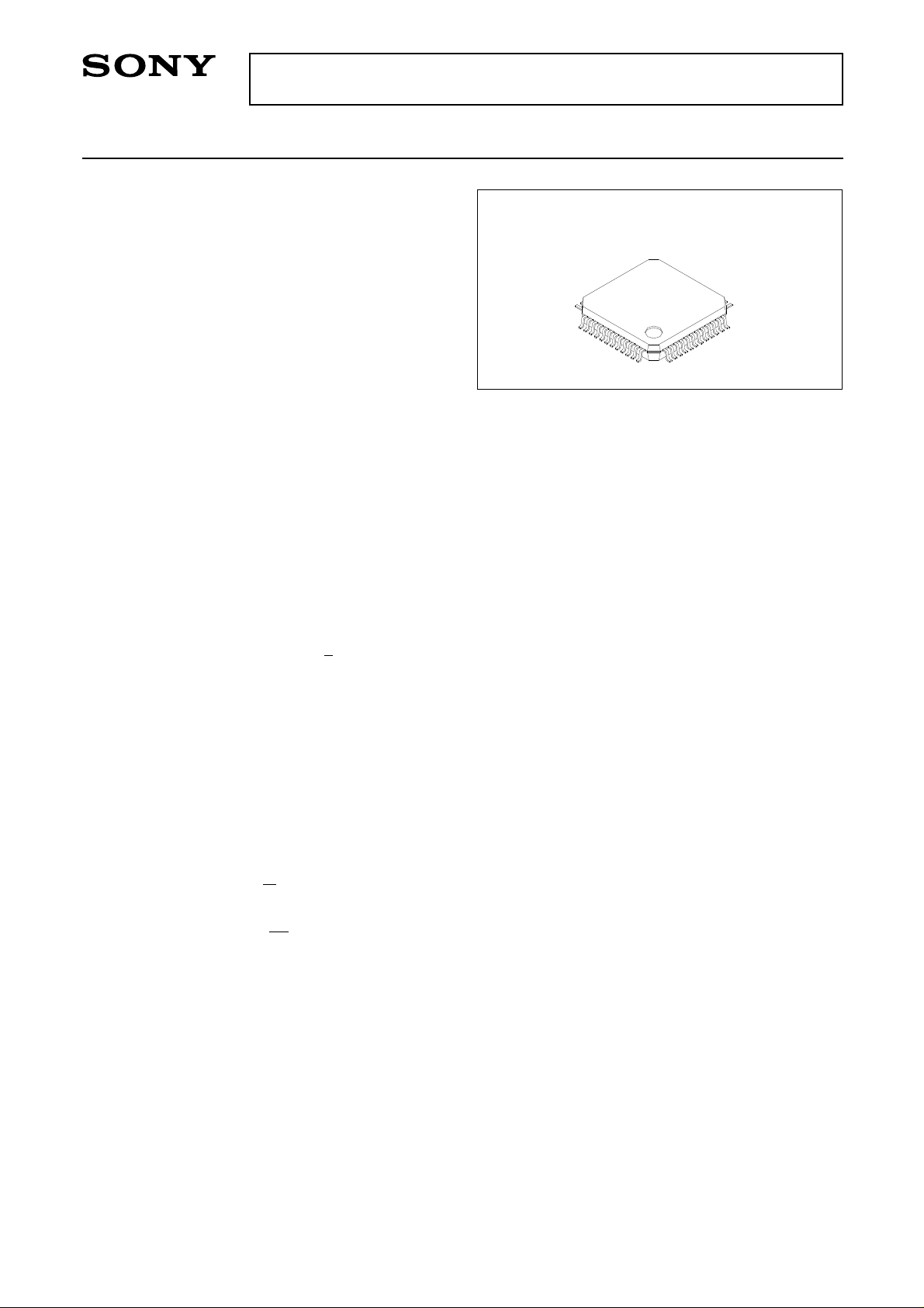
48 pin QFP (Plastic)
Absolute Maximum Ratings
• Power supply VCC – VEE –0.3 to +7.0 V
• Storage temperature Tstg –65 to +150 °C
• Input voltage difference: | VD – VD |
Vdif 0.0 to +2.5 V
• Input voltage Vi –0.3 to VCC V
• Output current
(Continuous) IO 0 to 50 mA
(Surge current) 0 to 100 mA
Recommended Operating Conditions
• Supply voltage VCC – VEE 5.0 ± 0.5 V
• Operating temperature Ta –40 to +85 °C
• Termination resistor (Q/Q)
RT1 45 to 55 Ω
• Termination resistor (SD/SD)
RT2 45 to 55 Ω
• Termination voltage VCC – VTT 1.8 to 2.2 V
Structure
Bipolar silicon monolithic IC
Sony reserves the right to change products and specifications without prior notice. This information does not convey any license by
any implication or otherwise under any patents or other right. Application circuits shown, if any, are typical examples illustrating the
operation of the devices. Sony cannot assume responsibility for any problems arising out of the use of these circuits.
– 1 –
E94709A63-ST

Block Diagram and Pin Configuration
CXB1567Q
VEE
N.C.
EED
V
CCD
V
EED
V
CCD
V
UP
DOWN
CCA
V
EEA
V
N.C.
N.C.
44
45
46
47
48
37
38
39
40
41
42
43
36
N.C.
35
N.C.
34
SD
Block
Alarm
33
SD
D
EE
V
32
31
Peak Hold1
Peak Hold2
D
EE
V
30
N.C.
29
R1
DA
CC
Q
28
V
Q
26
27
Buffer
Output
R3
R1
R2
EE
N.C.
V
25
N.C.
24
23
N.C.
Block
Limiting Amplifier Block
R3
20
19
18
17
16
15
14
13
22
21
EED
V
EED
V
EED
V
EED
V
EED
V
EED
V
CAP1
CAP1
N.C.
EE
V
R2
EE
V
2
N.C.
4
3
A
A
EE
CC
V
V
CAP3
CAP2
7
A
EE
V
6
5
9
8
D
10
D
N.C.
11
A
EE
V
121
N.C.
– 2 –

Pin Description
CXB1567Q
Pin
No.
1
2
3
4
5
6
Symbol
VEE
N.C.
VCCA
VEEA
CAP3
CAP2
Typical pin
voltage (V)
AC
DC
–
5V
0V
–
5V
–1.8V
–1.8V
Equivalent circuit
80
10p
40µA
Description
Negative power supply pin.
No connection.
Positive power supply pin for
analog block.
Negative power supply pin for
analog block.
5
6
80
Capacitance connection pins for
VCCA
alarm block peak hold circuit.
Connect each pin to VCC in
2000pF.
10p
CAP2 pin → Peak hold
capacitance
connection pin for
the limiting
amplifier signal
40µA
V
EEA
CAP3 pin → Peak hold
capacitance
connection pin for
the alarm
level setting block
7
8
9
10
11
12
13
14
15
16
17 to 22
23, 24
25
VEEA
D
N.C.
D
VEEA
N.C.
VEE
N.C.
CAP1
CAP1
VEED
N.C.
VEE
–
5V
–1.3V
–1.3V
–
5V
–
5V
–1.8V
–1.8V
–
5V
–
5V
–0.9V
to
–1.7V
10
Negative power supply pin for
analog block.
Limiting amplifier input pins
VCCA
Ensure that these inputs are
AC-coupled.
8
100
100
1K
7.5k
7.5k
130p
200
200
Negative power supply pin for
analog block.
16
15
No connection.
Negative power supply pin.
1K
V
EEA
No connection.
Capacitance connection pins to
determine the cut-off frequency
for feedback block.
Negative power supply pin for
digital block.
No connection.
Negative power supply pin.
– 3 –

Pin
No.
Symbol
Typical pin
voltage (V)
AC
DC
Equivalent circuit
CXB1567Q
Description
26
27
28
29
30
31, 32
33
34
N.C.
VCCDA
Q
Q
N.C.
VEED
SD
SD
0V
–5V
–0.9V
to
–1.7V
–0.9V
to
–1.7V
–0.9V
to
–1.7V
–0.9V
to
–1.7V
V
CCDA
VEED
V
CCDA
VEED
28
29
33
34
No connection.
Positive power supply pin for
output buffer.
Data signal output pins.
Terminate these pins in 50Ω at
VTT = –2V.
No connection.
Negative power supply pin for
digital block.
Alarm signal output pins.
Terminate these pins in 50Ω at
VTT = –2V.
35, 36
37
38
39
40
41
42
N.C.
VEE
N.C.
VEED
VCCD
VEED
VCCD
–5V
–5V
0V
–5V
0V
No connection.
Negative power supply pin.
No connection.
Negative power supply pin for
digital block.
Positive power supply pin for
digital block.
Negative power supply pin for
digital block.
Positive power supply pin for
digital block.
– 4 –

CXB1567Q
Pin
No.
43
44
45
46
47, 48
Symbol
UP
DOWN
VCCA
VEEA
N.C.
Typical pin
voltage (V)
DC
AC
–
4.7V
–5V
0V
–5V
43
44
Equivalent circuit
1k
100 100
5k
5k
VCCA
VEEA
Description
Resistor connection pins for alarm
level setting.
UP pin → When the
resistance
connected to this
pin is increased, the
alarm level
becomes higher.
DOWN pin →Normally
connect this pin
to VEE.
Positive power supply pin for
analog block.
Negative power supply pin for
analog block.
No connection.
– 5 –
 Loading...