


– 1 –
CXB1565R
E97323-PS
622Mbps Clock & Data Recovery with High Sensitivity Limitting Amplifier
Description
The CXB1565R achieves 3R optical-fiber communication receiver functions (Reshaping and Regenerating
and Retiming) on a single chip. This IC also equipped
with the signal interruption alarm output, which is
used to discriminate the existence of data input.
Features
• Auto-offset canceler circuit
• Signal interruption alarm output
• No reference clock required
• Single 5V power supply
Applications
• SONET/SDH: 622.08Mbps
• ATM: 622.08Mbps
Absolute Maximum Ratings
• Supply voltage VCC – VEE –0.3 to +7.0 V
• Storage temperature Tstg –65 to +150 °C
• Input voltage difference: | VD – VDN | Vdif 0 to 2.5 V
• TTL input voltage VinT –0.5 to 5.5 V
• Output current (Continuous) IO 0 to 50 mA
(Surge) 0 to 100 mA
Recommended Operating Conditions
• Supply voltage VCC – VEE 4.5 to 5.5 V
• Termination voltage (for RCK/RDATA) VCC – VT1 1.8 to 2.2 V
• Termination voltage (for SDE) VT2 VEE V
• Termination resistance (for RCK/RDATA) RT1 46 to 56 Ω
• Termination resistance (for SDE) RT2 460 to 560 Ω
• Operating temperature Ta –40 to +85 °C
Sony reserves the right to change products and specifications without prior notice. This information does not convey any license by
any implication or otherwise under any patents or other right. Application circuits shown, if any, are typical examples illustrating the
operation of the devices. Sony cannot assume responsibility for any problems arising out of the use of these circuits.
64 pin LQFP (Plastic)
For the availability of this product, please contact the sales office.
– 2 –
CXB1565R
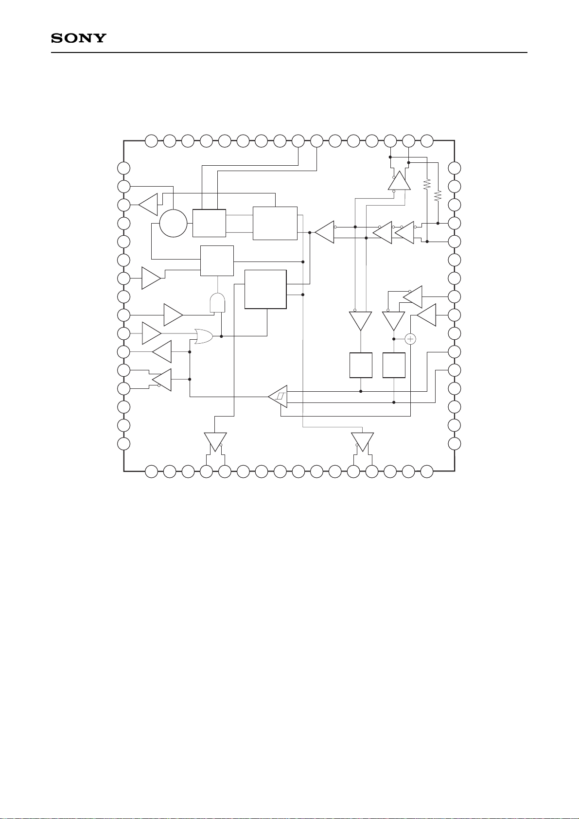
Block Diagram and Pin Configuration
NC
NC
REXT
LKDT
V
EEG
V
EEG
V
CCG
EXCK
NC
CKSEL
SQLCH
SDC
SDE
SDEN
NC
NC
NC
V
EE
P1
V
EE
P1
NC
NC
NC
NC
V
EE
P2
LPFB
LPFA
V
CC
P
V
CC
P
NC
CAP1B
CAP1
V
EE
R1
NC
V
EER2
V
EER2
DN
D
V
CCR1
V
CCR2
DOWN
HYS
V
EER3
CAP2
CAP3
NC
NC
NC
NC
NC
V
CC
E1
V
CC
E1
RDATA
RDATAN
V
EE
E1
V
EE
G
V
EE
G
V
CC
G
V
CC
G
V
EE
E2
RCKN
RCK
V
CC
E2
V
CC
E2
NC
charge
pump
VCO
peak
hold
phase/
frequency
detector
Mux.
1
0
Reset
D
CK
D-FF
Up
Down
peak
hold
17
18
19
20
21
22
23
24
25
26
27
28
29
30
31
32
40
39
38
37
36
35
34
33
41
42
43
44
45
46
47
48
49
50
51
52
53
54
55
56
57
58
59
60
63
64
61
62
2
3
4
5
6
7
8
9
10
11
12
13
14
15
16
1
– 3 –
CXB1565R
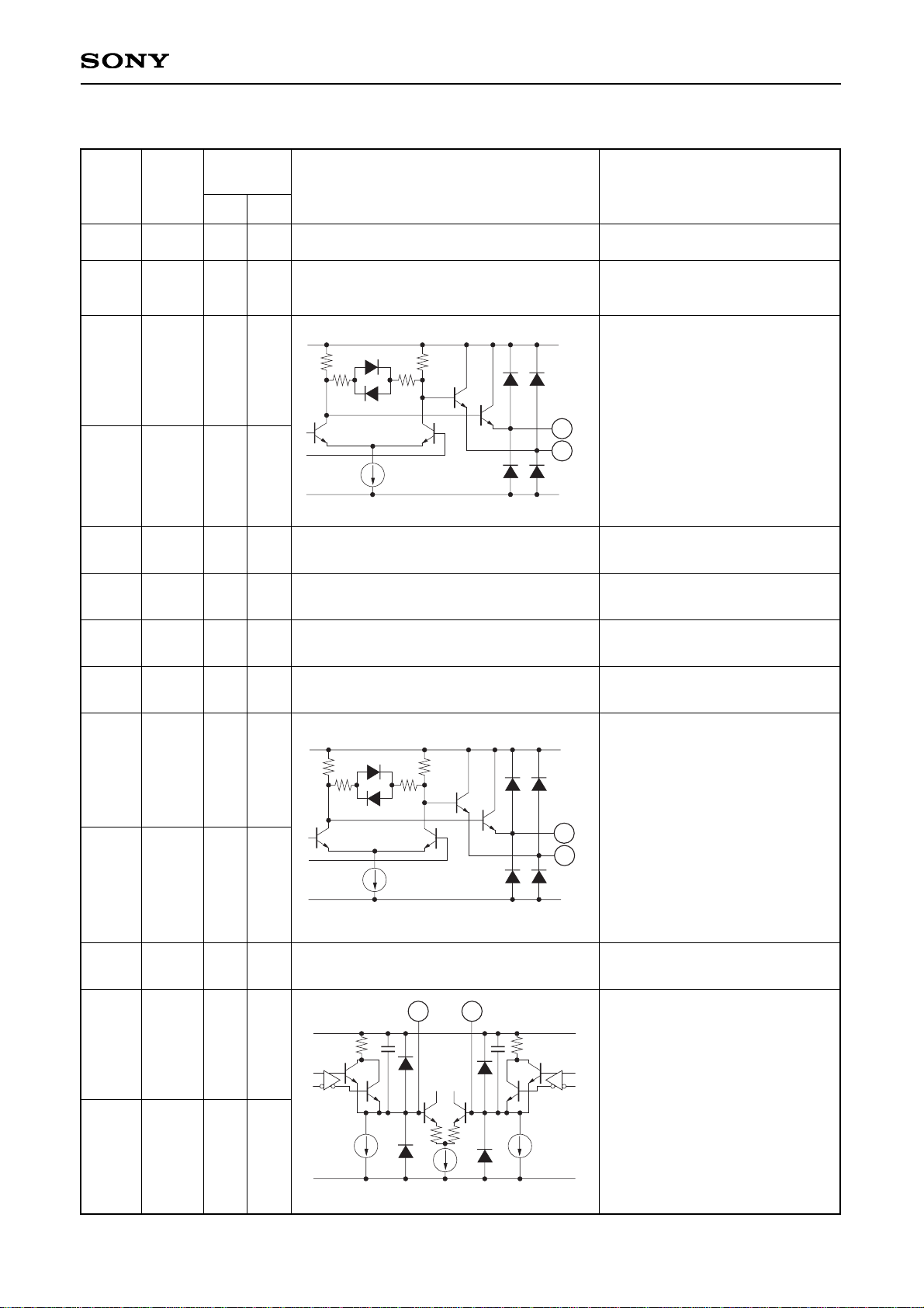
Pin No.
2, 3
VCCE1
5
1,
16 to 20
NC
No connect
11
VEEE2
0
Ground for RCK/RCKN outputs
circuits.
6
VEEE1
0
Ground for RDATA/RDATAN
output circuits.
14, 15
VCCE2
5
Positive supply for RCK/RCKN
output circuits.
7, 8
52, 53
VEEG
0
Ground for digital circuits.
9, 10
54
VCCG
5
Positive supply for digital circuits.
Positive supply for
RDATA/RDATAN output circuits.
4
RDATA
3.3
to
4.1
5
RDATAN
3.3
to
4.1
Retimed data outputs.
Symbol
Typical pin
voltage (V)
DC
AC
Equivalent circuit
Description
VCCE1
V
EEE1
4
5
12
RCKN
3.3
to
4.1
13
RCK
3.3
to
4.1
21
CAP3
3.2
22
CAP2
3.2
Recovered clock outputs.
VCCE2
VEEE2
12
13
Connect a peak hold capacitor
for signal detector.
Typically 470pF.
VCCR2
VEER3
10p
5µA 5µA
21
22
Pin Description
– 4 –
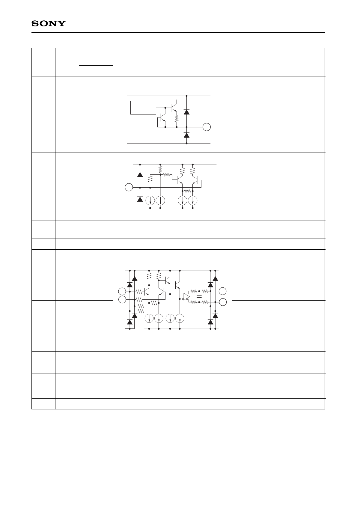
CXB1565R
Pin No.
23
VEER3
0
24
HYS
0.3
Ground for signal detector.
Connect to VEER3 through a
external resistor determine
signal detect hysteresis width
(∆P).
When connect to VEER3 directly.
∆P ≈ 6dB (Typ.)
When 8.2kΩ is inserted.
∆P ≈ 3dB (Typ.)
Symbol
Typical pin
voltage (V)
DC
AC
Equivalent circuit
Description
VCCR2
V
EER3
Bias
Generator
24
25
DOWN
4.4
26 VCCR2 5
28
D
29
DN
34
CAP1
3.7
35
CAP1B
3.7
Connect to VCCR2 through a
external resistor to decrease
signal detect level (SDL). When
open, SDL sets to 20mVp-p.
(single-ended)
Positive supply for signal
detector.
27
VCCR1 0
Positive supply for post amplifier.
30, 31
VEER2 0
Ground for post amplifier.
Serial data stream inputs.
Connect a external capacitor,
which determines low cut-off
frequency for feedback block.
Typically 0.022µF.
VCCR2
V
EER3
25
VCCR1
V
EER2VEER1
28
29
34
35
32, 36
NC
33
VEER1
0
No connect
37, 38
VCCP
5
Positive supply for PLL circuits.
Ground for post amplifier.
Both VEER1 and VEER2 must be
grounded.
– 5 –
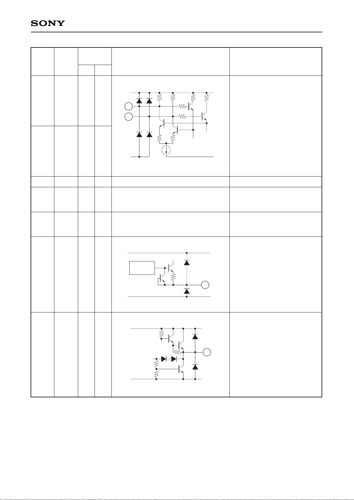
CXB1565R
Pin No.
39
LPFA
40
LPFB
41
VEEP2
0
Connect a external loop filter
capacitor.
Typically 0.33µF.
Ground for PLL circuits.
42 to 45
48, 49
56
NC
46, 47
VEEP1
0
Ground for PLL circuits.
Both VEEP1 and VEEP2 must be
grounded.
50
REXT
0.6
Connect to VEEP1 through a
external resistor to determine
VCO frequency.
Typically 2.4kΩ.
No connect
Symbol
Typical pin
voltage (V)
DC
AC
Equivalent circuit
Description
VCCP
V
EEP1VEEP2
39
40
VCCP
V
EEP2
Bias
Generator
50
51 LKDT
Lock detector (TTL).
Driven low, while synchronization
is lost.
If SQLCH is asserted(low),fixed
high even when lock is lost.
0.2
to
4.8
VCCG
V
EEG
51
 Loading...