

Sony CXB1563Q Datasheet

Description
The CXB1563Q achieves the 2R optical-fiber
communication receiver functions (Reshaping and
Regenerating) on a single chip. This IC is also
equipped with the signal interruption alarm output
function, which is used to discriminate the existence
of data input.
Features
• Auto-offset canceler circuit
• Signal interruption alarm output
• 2-level switching function of identification maximum voltage amplitude for alarm block
• Single 5V power supply
Applications
• SONET/SDH : 622.08Mb/s
• Fiber channel : 531.25Mb/s
Absolute Maximum Ratings
• Supply voltage VCC – VEE –0.3 to +7.0 V
• Storage temperature Tstg –65 to +150 °C
• Input voltage difference : I VD – VD I Vdif 0.0 to +2.5 V
• SW input voltage Vi VEE to VCC V
• Output current (Continuous) IO 0 to 50 mA
(Surge current) 0 to 100 mA
Recommended Operating Conditions
• Supply voltage VCC – VEE 5.0±0.5 V
• Termination voltage (for data/alarm) VCC – VT1 1.8 to 2.2 V
• Termination voltage (for alarm 2) VT2 VEE V
• Termination resistance (for data/alarm)RT1 45 to 55 Ω
• Termination resistance (for alarm 2) RT2 460 to 560 Ω
• Operating temperature Ta –40 to +85 °C
Structure
Bipolar silicon monolithic IC
– 1 –
CXB1563Q
E95710A6Z
2R IC for Optical Fiber Communication Receiver
Sony reserves the right to change products and specifications without prior notice. This information does not convey any license by
any implication or otherwise under any patents or other right. Application circuits shown, if any, are typical examples illustrating the
operation of the devices. Sony cannot assume responsibility for any problems arising out of the use of these circuits.
32 pin QFP (Plastic)
– 2 –
CXB1563Q
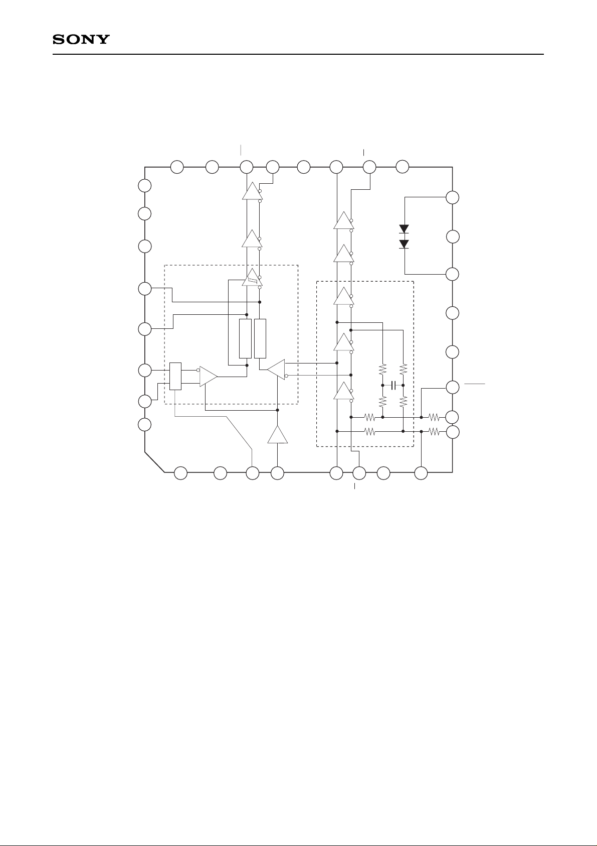
Block Diagram and Pin Configuration
2
3
4
5
6
7
8
9
10
11
12
13
14
15
16
17
18
19
20
21
22
23
24
25
26
27
28
29
30
31
32
1
peak hold
∆V
peak hold
Alarm
Block
Limiting
Amplifier
Block
R1
R1
R2
R2
Q
VccDA
SD
Q
SD
VccD
VccDA
N.C.
N.C.
CAP3
CAP2
DOWN
UP
VccA
TM
VccD
V
EED
VccA
V
EEA
CAP1
R2K
R1K
VccA
VccA
V
EE
I
SW
D
D
CAP1
N.C.
R3
R4
V
CC
A
N.C.

– 3 –
CXB1563Q
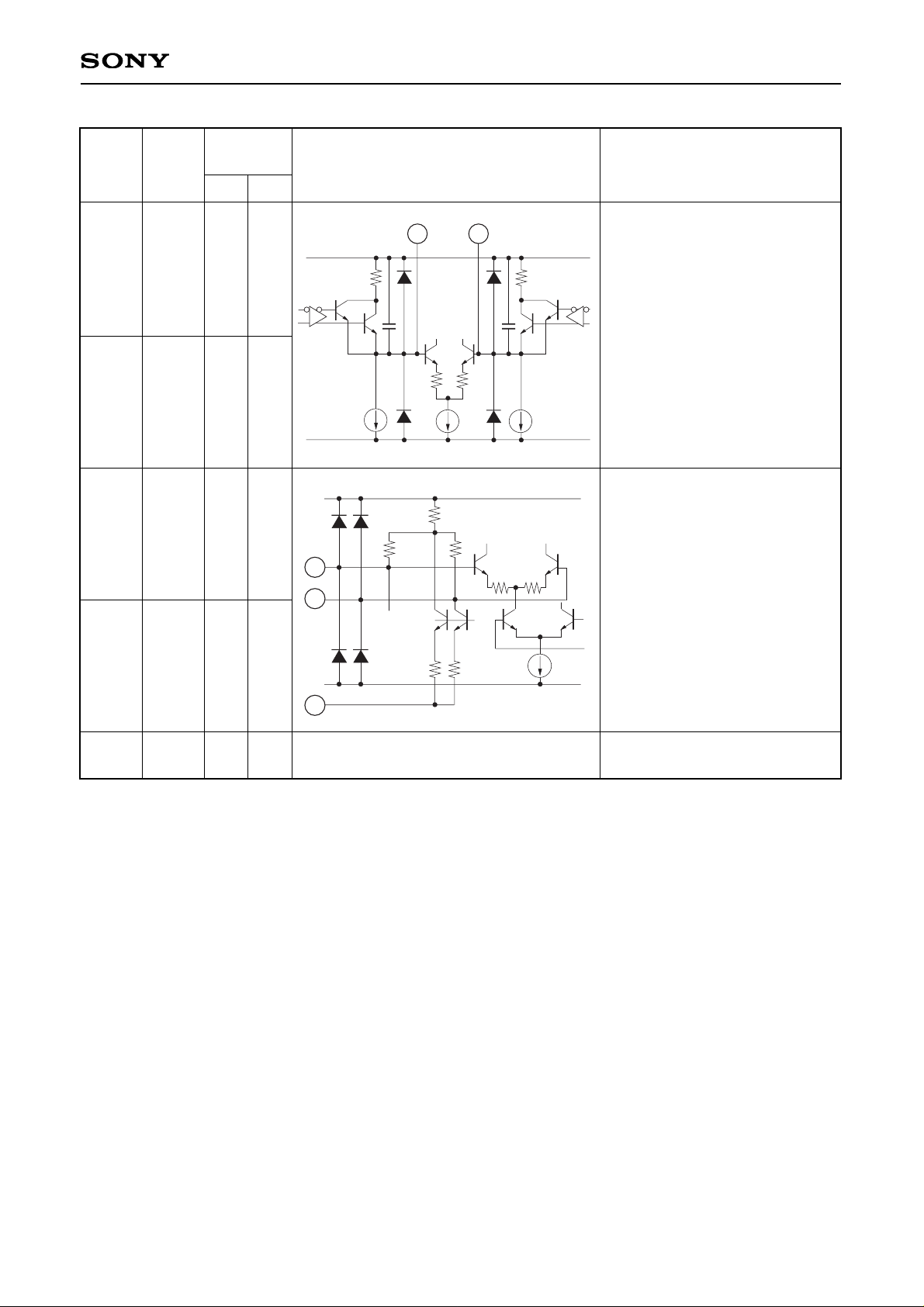
Pin Description
Pin No.
1,2
VCCA
0V
Positive power supply for analog
block.
Switches the identification
maximum voltage amplitude.
High voltage when open; the
identification maximum voltage
amplitude becomes 50mVp-p.
Low voltage when connecting
this pin to VEE; the amplitude
becomes 20mVp-p.
3 VEEI –5V
4
SW
0V
(OPEN)
or
–5V
Limiting amplifier block input.
Be sure to make this input with
AC coupled.
Positive power supply for analog
block.
Pins 8 and 11 connect a
capacitor which determines the
cut-off frequency for feedback
block, and 1kΩ is connected
between Pins 8 and 9; 2kΩ
between Pins 10 and 11. A
resistor which is to be inserted in
parallel with a capacitor can be
selected 5 ways by external
wiring, and DC feedback can be
varied.
5
D
–
1.3V
–
0.9V
to
–
1.7V
–
0.9V
to
–
1.7V
6
D
–
1.3V
7
VCCA
0V
8
CAP1
–
1.8V
9
R1K
10
R2K
11
CAP1
–
1.8V
Generates the default voltage
between UP and DOWN.
The voltage (8.0mV for input
conversion) can be generated
between UP and DOWN
(Pins 30 and 31) as alarm
setting level by connecting this
pin to VEEA.
Symbol
Typical pin
voltage (V)
DC
AC
Equivalent circuit
Description
150k
100k
V
REF
VEEA
V
CCA
4
31
30
VccA
V
EEA
SW
993
110.3
110.3
Vcs
3
VCCA
V
EEA
200
200
1.5k
1.5k
10k
10k
100p
200
200
2k
1k
5
6
11
10
9
8

– 4 –
CXB1563Q
12
13
14
15
VEEA
VCCA
VEED
VCCD
–5V
0V
–5V
0V
–
0.9V
to
–
1.7V
Negative power supply for
analog block.
Positive power supply for analog
block.
Negative power supply for digital
block.
Positive power supply for digital
block.
16
TM
–
3.4V
18
Q
–
0.9V
to
–
1.7V
19
Q
Positive power supply for output
buffer.
20
VCCDA
Chip temperature monitor.
17
N.C
No connected.
Data signal output.
Terminate this pin in 50Ω at
VTT = –2V.
–
0.9V
to
–
1.7V
21
SD
Alarm signal output.
Terminate this pin in 50Ω at
VTT = –2V.
DC
AC
14
16
–
0.9V
to
–
1.7V
22
SD
23
24
25
26
27
VccDA
VccD
N.C
N.C
N.C
Positive power supply for digital
block.
Positive power supply for digital
block.
No connected.
0V
0V
0V
VEED
V
CCDA
19
18
VEED
V
CCDA
21
22
Pin No.
Symbol
Typical pin
voltage (V)
Equivalent circuit
Description
– 5 –
CXB1563Q
DC
AC
28
CAP3
–
1.8V
29
CAP2
–
1.8V
Connects a peak hold circuit
capacitor for alarm block. 470pF
should be connected to VccA
each.
CAP2 pin → Peak hold
capacitor connection for
alarm level setting block.
CAP3 pin → Peak hold
capacitor connection for
limiting amplifier signal.
10p
10p
VCCA
V
EEA
80
5µA
5µA
80
29
28
30
DOWN
–
0.84V
(for
VEEI
= –5V)
31
UP
–
0.8V
(for
VEEI
= –5V)
32
VccA
0V
Positive power supply for analog
block.
Connects a resistor for alarm
level setting.
Default voltage can be
generated without an external
resistor by shorting the VEEI pin
to VEEA.
31
30
VccA
V
EEA
SW
993
110.3
110.3
Vcs
3
Pin No.
Symbol
Typical pin
voltage (V)
Equivalent circuit
Description
 Loading...